

TLE6288R
Smart 6 Channel Peak & Hold Switch
Data Sheet, Rev. 2.5, Oct. 2010
Automotive Power

Data Sheet
2
Rev. 2.5, 2010-10-11
TLE6288R
Table of Contents
Table of Contents . . . . . . . . . . . . . . . . . . . . . . . . . . . . . . . . . . . . . . . . . . . . . . . . . . . . . . . . . . . . . . . . 2
1
Block Diagram . . . . . . . . . . . . . . . . . . . . . . . . . . . . . . . . . . . . . . . . . . . . . . . . . . . . . . . . . . . . . . . . . . . 4
2
Pin Configuration . . . . . . . . . . . . . . . . . . . . . . . . . . . . . . . . . . . . . . . . . . . . . . . . . . . . . . . . . . . . . . . . 5
2.1
Pin Assignment . . . . . . . . . . . . . . . . . . . . . . . . . . . . . . . . . . . . . . . . . . . . . . . . . . . . . . . . . . . . . . . . . . . 5
2.2
Pin Definitions and Functions . . . . . . . . . . . . . . . . . . . . . . . . . . . . . . . . . . . . . . . . . . . . . . . . . . . . . . . . 5
2.3
Pin Description . . . . . . . . . . . . . . . . . . . . . . . . . . . . . . . . . . . . . . . . . . . . . . . . . . . . . . . . . . . . . . . . . . . 6
3
General Product Characteristics . . . . . . . . . . . . . . . . . . . . . . . . . . . . . . . . . . . . . . . . . . . . . . . . . . . . 8
3.1
Absolute Maximum Ratings . . . . . . . . . . . . . . . . . . . . . . . . . . . . . . . . . . . . . . . . . . . . . . . . . . . . . . . . . 8
3.2
Thermal Resistance . . . . . . . . . . . . . . . . . . . . . . . . . . . . . . . . . . . . . . . . . . . . . . . . . . . . . . . . . . . . . . . 9
4
Description . . . . . . . . . . . . . . . . . . . . . . . . . . . . . . . . . . . . . . . . . . . . . . . . . . . . . . . . . . . . . . . . . . . . 10
4.1
Gerneral Functional Description . . . . . . . . . . . . . . . . . . . . . . . . . . . . . . . . . . . . . . . . . . . . . . . . . . . . . 10
4.1.1
Output Stage Control: Parallel Control and SPI Control . . . . . . . . . . . . . . . . . . . . . . . . . . . . . . . . . 10
4.1.2
Current Regulator: Peak Current Control with Fixed Off-Time . . . . . . . . . . . . . . . . . . . . . . . . . . . . 11
4.2
Protection . . . . . . . . . . . . . . . . . . . . . . . . . . . . . . . . . . . . . . . . . . . . . . . . . . . . . . . . . . . . . . . . . . . . . . 13
4.3
Diagnostic . . . . . . . . . . . . . . . . . . . . . . . . . . . . . . . . . . . . . . . . . . . . . . . . . . . . . . . . . . . . . . . . . . . . . . 14
4.3.1
Parallel Diagnostic Functions . . . . . . . . . . . . . . . . . . . . . . . . . . . . . . . . . . . . . . . . . . . . . . . . . . . . . 14
4.3.2
Electrical Characteristics: Diagnostic Functions . . . . . . . . . . . . . . . . . . . . . . . . . . . . . . . . . . . . . . . 14
5
SPI . . . . . . . . . . . . . . . . . . . . . . . . . . . . . . . . . . . . . . . . . . . . . . . . . . . . . . . . . . . . . . . . . . . . . . . . . . . 15
5.1
SPI Signal Description . . . . . . . . . . . . . . . . . . . . . . . . . . . . . . . . . . . . . . . . . . . . . . . . . . . . . . . . . . . . 15
5.2
Electrical Characteristics: SPI Timing . . . . . . . . . . . . . . . . . . . . . . . . . . . . . . . . . . . . . . . . . . . . . . . . . 16
5.3
SPI Diagnostics . . . . . . . . . . . . . . . . . . . . . . . . . . . . . . . . . . . . . . . . . . . . . . . . . . . . . . . . . . . . . . . . . 17
5.4
SPI Commands, Values and Parameters . . . . . . . . . . . . . . . . . . . . . . . . . . . . . . . . . . . . . . . . . . . . . . 18
5.5
SPI Commands . . . . . . . . . . . . . . . . . . . . . . . . . . . . . . . . . . . . . . . . . . . . . . . . . . . . . . . . . . . . . . . . . . 19
5.6
Bit Assignment and Default Settings for Internal Logic Registers . . . . . . . . . . . . . . . . . . . . . . . . . . . 21
5.7
SPI Timing Diagrams . . . . . . . . . . . . . . . . . . . . . . . . . . . . . . . . . . . . . . . . . . . . . . . . . . . . . . . . . . . . . 22
6
Electrical Characteristics Input / Output Pins . . . . . . . . . . . . . . . . . . . . . . . . . . . . . . . . . . . . . . . . 24
6.1
Power Supply, Reset . . . . . . . . . . . . . . . . . . . . . . . . . . . . . . . . . . . . . . . . . . . . . . . . . . . . . . . . . . . . . 24
6.2
Power Outputs . . . . . . . . . . . . . . . . . . . . . . . . . . . . . . . . . . . . . . . . . . . . . . . . . . . . . . . . . . . . . . . . . . 24
6.3
Digital Inputs . . . . . . . . . . . . . . . . . . . . . . . . . . . . . . . . . . . . . . . . . . . . . . . . . . . . . . . . . . . . . . . . . . . . 25
6.4
Digital Outputs . . . . . . . . . . . . . . . . . . . . . . . . . . . . . . . . . . . . . . . . . . . . . . . . . . . . . . . . . . . . . . . . . . 26
7
Application Information . . . . . . . . . . . . . . . . . . . . . . . . . . . . . . . . . . . . . . . . . . . . . . . . . . . . . . . . . . 27
7.1
Z
thjc
Diagram Junction - Case for Single channel operation . . . . . . . . . . . . . . . . . . . . . . . . . . . . . . . . 27
7.2
Thermal Application Information . . . . . . . . . . . . . . . . . . . . . . . . . . . . . . . . . . . . . . . . . . . . . . . . . . . . . 27
7.3
Overload/Low Inductance Load Detection in Current Regulation Mode . . . . . . . . . . . . . . . . . . . . . . . 29
8
Package Outlines . . . . . . . . . . . . . . . . . . . . . . . . . . . . . . . . . . . . . . . . . . . . . . . . . . . . . . . . . . . . . . . 30
9
Revision History . . . . . . . . . . . . . . . . . . . . . . . . . . . . . . . . . . . . . . . . . . . . . . . . . . . . . . . . . . . . . . . . 31
Table of Contents
Data Sheet
3
Rev. 2.5, 2010-10-11
Type
Package
TLE6288R
PG-DSO-36-54
TLE6288R
Features
•
3 Channel high side with adjustable Peak & Hold current
control
•
3 Channel high/low side configurable
•
Protection
– Overcurrent (current limitation)
– Overtemperature
– Overvoltage (active clamping)
•
Diagnosis
– Overcurrent
– Overtemperature
– Open load (Off-State)
– Short to Ground (Off-state, lowside configuration)
– Short to
V
B
(Off-state, highside configuration)
•
Interface and Control
– 16-Bit Serial Peripheral Interface (2 bit/CH)
– Device programming via SPI
– Separate diagnosis output for each CH (DIAG1
to 6)
– General Fault Flag + Overtemperature Flag
– Direct parallel control of all channels
– General enable signal to control all channels
simultaneously
•
Low Quiescent Current
•
Compatible with 3.3 V and 5 V microcontrollers
•
Electrostatic discharge (ESD) protection of all pins
•
Green Product (RoHS compliant)
•
AEC Qualified
Application
•
Peak & Hold Loads (valves, coils)
•
Solenoids, Relays and Resistive Loads
•
Fast protected Highside Switching
(PWM up to > 10 kHz)
General Description
The TLE6288R is a 6-channel (150 m
Ω) Smart Multichannel Switch in Smart Power Technology. The IC has
embedded protection, diagnosis and configurable functions. Channels 1-3 are highside channels with integrated
charge pump and can be programmed individually to do autonomous peak and hold current regulation with PWM.
Channel 4-6 (also with integrated charge pump) can be configured to work as highside switch or lowside switch.
This IC can be used to drive standard automotive loads in highside or lowside applications with switching
frequencies up to 10 kHz. In addition the TLE6288R can be used to drive autonomously up to 3 inductive
peak & hold (valves, coils) loads with programmable peak and hold current values.
Table 1
Product Summary
Parameter
Symbol
Values
Unit
Logic Supply voltage
V
CC
4.5 … 5.5
V
On resistance
R
DS(ON)1-6
0.15 typ. @ 25 °C
Ω
Lowside clamping voltage
V
cll(max)
+55
V
Highside clamping voltage
V
clh(max)
-19
V
Peak current range
I
pk
1.2 … 3.6
A
Hold current range
I
hd
0.7 … 2
A
Peak time range
I
p
0 … 3.6
ms
Fixed off time range
I
fo
100 … 400
μs
TLE6288R
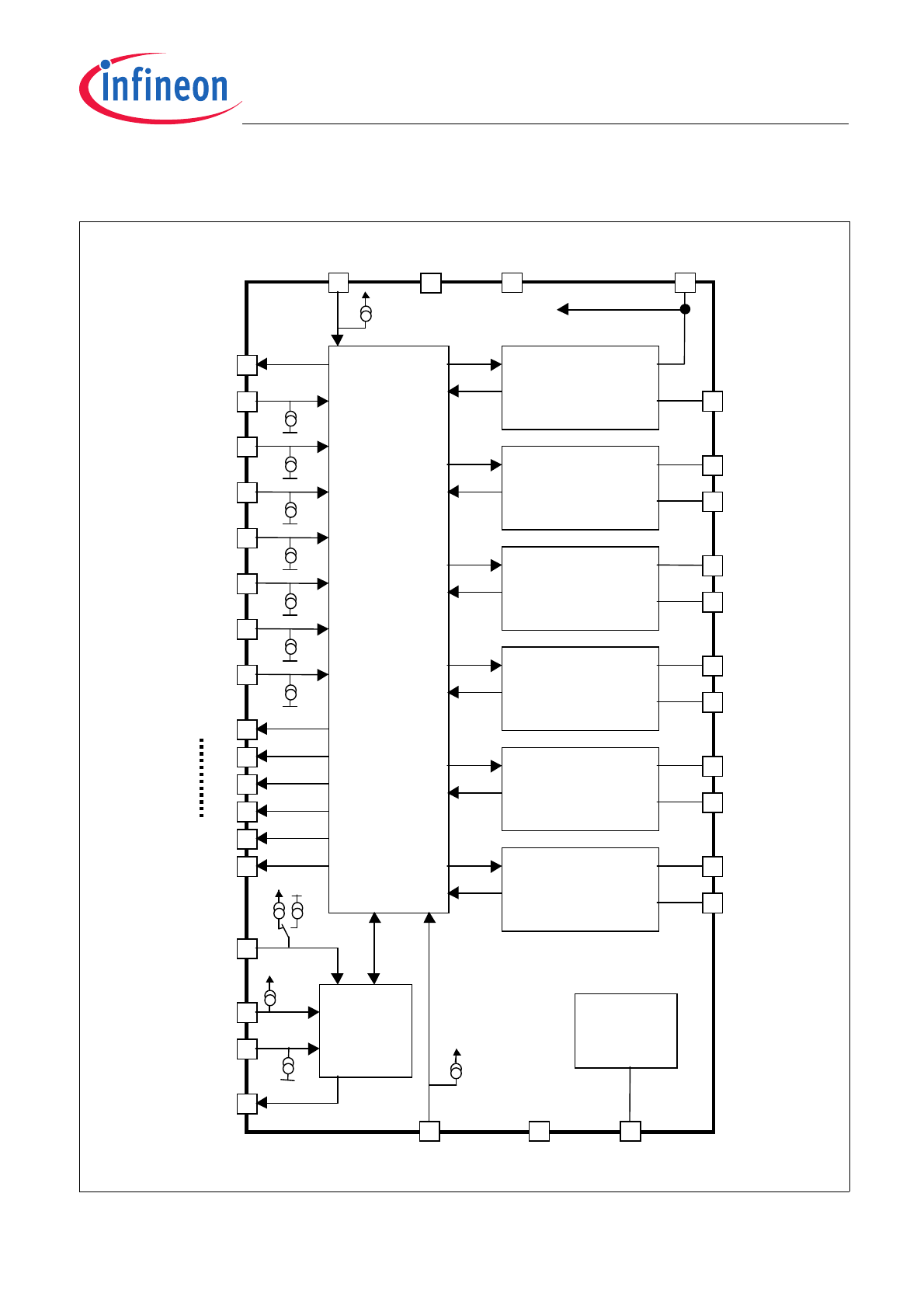
Block Diagram
Data Sheet
4
Rev. 2.5, 2010-10-11
1
Block Diagram
Figure 1
Block Diagram
Charge
pump
VCP
GND
FSIN
Channel 3
Highside 300 mΩ
Peak&Hold
Channel 2
Highside 300 mΩ
Peak&Hold
Channel 1
Highside 300 mΩ
Peak&Hold
Channel 4
Highside/ Lowside
300 mΩ
Channel 5
Highside/ Lowside
300 mΩ
Channel 6
Highside/ Lowside
300 mΩ
VB
VCC
DOUT 3 / VB
SOUT 3
SOUT 2
SOUT 1
DOUT 4
SOUT 4
DOUT 5
SOUT 5
DOUT 6
SOUT 6
SPI
SCLK
CS
SI
SO
Logic
Driver
Diagnosis
IN 1
DIAG 1
IN 2
IN 3
IN 4
IN 5
DIAG 5
IN 6
DIAG 6
Overtemp.
Reset
VDO
CLKProg
Fault
.
.
Vcc
Vcc
.
Vcc
.
.
Vcc
.
.
.
.
.
.
.
GND
GND
DOUT 2
DOUT 1
Data Sheet
5
Rev. 2.5, 2010-10-11
TLE6288R
Pin Configuration
2
Pin Configuration
2.1
Pin Assignment
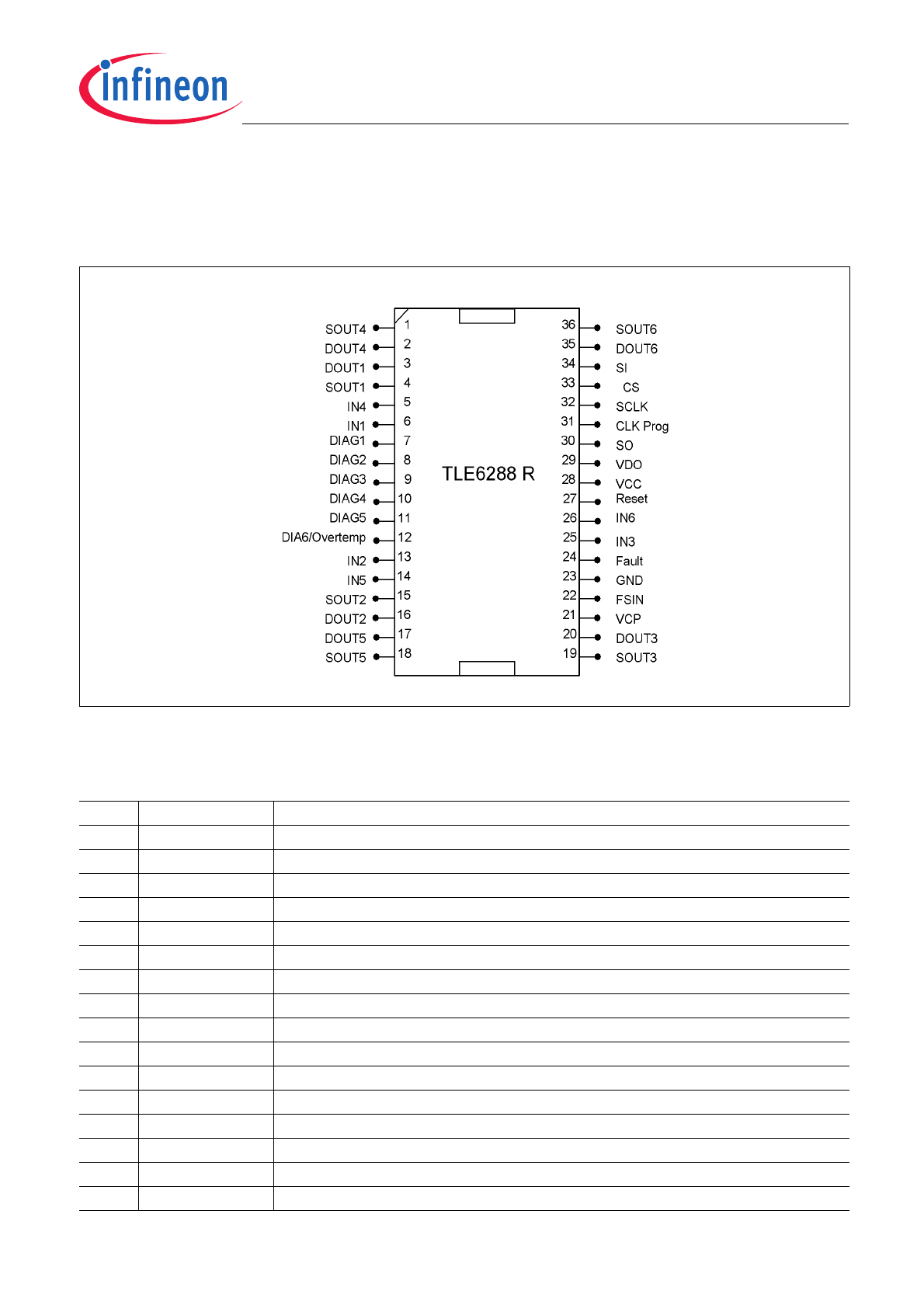
Figure 2
Pin Configuration PG-DSO-36-54
2.2
Pin Definitions and Functions
Pin
Symbol
Function
1
SOUT4
Source Output CH 4 (high/low side)
2
DOUT4
Drain Output CH 4 (high/low side)
3
DOUT1
Drain Output CH 1 (high side)
4
SOUT1
Source Output CH 1 (high side)
5
IN4
Control Input Channel 4
6
IN1
Control Input Channel 1
7
DIAG1
Diagnostic Output CH 1
8
DIAG2
Diagnostic Output CH 2
9
DIAG3
Diagnostic Output CH 3
10
DIAG4
Diagnostic Output CH 4
11
DIAG5
Diagnostic Output CH 5
12
DIAG6/Overtemp Diagnostic Output CH 6 / Overtemp
13
IN2
Control Input Channel 2
14
IN5
Control Input Channel 5
15
SOUT2
Source Output CH 2 (high side)
16
DOUT2
Drain Output CH 2 (high side)
TLE6288R
Pin Configuration
Data Sheet
6
Rev. 2.5, 2010-10-11
2.3
Pin Description
17
DOUT5
Drain Output CH 5 (high/low side)
18
SOUT5
Source Output CH 5 (high/low side)
19
SOUT3
Source Output CH 3 (high side)
20
DOUT3
Drain Output CH 3 (high side)
21
VCP
Charge Pump capacitor pin
22
FSIN
All Channels Enable/Disable
23
GND
Logic Ground
24
Fault
General Fault Flag
25
IN3
Control Input Channel 3
26
IN6
Control Input Channel 6
27
Reset
Reset pin (+ Standby Mode)
28
V
CC
Logic Supply Voltage (5 V)
29
V
DO
Supply pin for digital outputs
30
SO
SPI Serial Data Output
31
CLKProg
Program pin of SPI Clock
32
SCLK
SPI Serial Clock
33
CS
SPI Chip Select
34
SI
SPI Serial Data Input
35
DOUT6
Drain Output CH 6 (high/low side)
36
SOUT6
Source Output CH 6 (high/low side)
Symbol
Description
DOUT1-3 Drain of the 3 highside channels. These pins must always be connected to the same power (battery)
supply line (
V
B
).
SOUT1-3 Source of the 3 highside channels. Outputs of the highside channels where the load is connected.
DOUT4-6 Drain pins of the 3 configurable channels. In highside configuration they must be connected to the
same voltage as DOUT1-3. In lowside configuration they are the output pins and connected to the
load.
SOUT4-6 Source of the 3 configurable channels. In highside configuration they are the outputs and connected
to the load. In lowside configuration they must be connected with GND.
IN1-6
Parallel input pins for the 6 power outputs. These pins have an internal pull-down structure.
GND
Logic ground pin, the heat slug has to be connected to this potential.
FSIN
Disable pin. If the FSIN pin is in a logic low state, it switches all outputs OFF. The pin has an internal
pull-up structure.
Reset
Reset pin. When the reset is low all channels are off, the internal biasing is deactivated, all internal
registers are cleared and the supply-current consumption is reduced (standby mode). The pin has an
internal pull-up structure.
Fault
General Fault pin. There is a general fault pin (open drain) which shows a high to low transition as
soon as an error is latched into the diagnosis register. When the diagnosis register is cleared this flag
is also reset (high ohmic). This fault indication can be used to generate a
μC interrupt.
Pin
Symbol
Function

Data Sheet
7
Rev. 2.5, 2010-10-11
TLE6288R
Pin Configuration
For more details about the SPI see
Chapter 5
.
CLKProg Programming pin for the SPI Clock signal. This pin can be used to configure the clock signal input of
the SPI. In low state the SPI will read data at the rising clock edge and write data at the falling clock
edge. In high state the SPI will read data at the falling clock edge and write data at the rising clock
edge. The pin has an internal pull-down structure.
DIAG1-5
Parallel diagnostic pins (push-pull) change state according to the input signal of the corresponding
channel. For further details refer to
Chapter 4.3.1
DIAG6/
Overtemp
VCP
Pin to connect the external capacitor of the integrated charge pump. Connect a ceramic capacitor with
47 nF between this pin and DOUT3 (
V
B
).
V
DO
Supply pin of the push-pull digital output drivers. This pin can be used to vary the high-state output
voltage of the SO pin and the DIAG1-6 pins.
V
CC
Logic supply pin. This pin is used to supply the integrated circuitry.
CS
Chip Select of the SPI (active low)
SO
Signal Output of the Serial Peripheral Interface
SI
Signal Input of the Serial Peripheral Interface. The pin has an internal pull-down structure.
SCLK
Clock Input of the Serial Peripheral Interface. The pin has an internal pull-up structure
(if CLKProg = L) or an pull-down structure (if CLKProg = H).
Symbol
Description
TLE6288R
General Product Characteristics
Data Sheet
8
Rev. 2.5, 2010-10-11
3
General Product Characteristics
3.1
Absolute Maximum Ratings
Attention: Stresses above the ones listed here may cause permanent damage to the device. Exposure to
absolute maximum rating conditions for extended periods may affect device reliability.
Absolute Maximum Ratings
1)
T
j
= -40
⋅C to +150 ⋅C; all voltages with respect to ground, positive current flowing into pin
(unless otherwise specified)
1) Not subject to production test, specified by design.
Pos.
Parameter
Symbol
Limit Values
Unit
PIN / Conditions
Min.
Max.
Voltages
3.1.1
Power Supply Voltage 1 static
dynamic: 1 min. 25
°C
dynamic: Test cond. see
Figure 3
V
B
V
B
V
B
-0.3
–
–
20
24
40
V
DOUT1-3
DOUT1-3
2)
DOUT1-3
2)
2) As long as max. junction temperature
T
j
is not exceeded.
3.1.2
Power Supply Voltage 2
V
CC
V
DO
-0.3
7
V
VCC
VDO
3.1.3
Continuous Drain Source Voltage
(lowside configuration)
V
DSL
–
40
V
DOUT - SOUT
(channel 4 to 6)
Continuous Source Voltage
(highside configuration)
V
SH
-9
V
B
V
SOUT - GND
(channel 4 to 6)
3.1.4
Input Voltage
V
IN
-0.3
V
CC
+ 0.3 V
IN1-6, Reset,
FSIN, CS, SCLK,
SI, CLKProg
3.1.5
Output Voltage
V
OUT
-0.3
V
CC
+ 0.3 V
Fault
DIAG1-6
SO
3.1.6
Output Voltage
V
CP
–
V
B
+ 10
V
VCP; no voltage
must be applied
Currents
3.1.7
Reverse Current (1 ms)
I
rev
-4
–
A
between DOUT
and SOUT;
Channel 4 to 6
Temperatures
3.1.8
Operating Temperature
T
j
-40
+150
°C
–
3.1.9
Storage Temperature
T
stg
-55 +150
°C
–
ESD Susceptibility
3.1.10
ESD (Human Body Model)
C
= 100 pF,
R
= 1.5 k
Ω
Applied to all terminals 3 times
V
ESDb
–
2000
V
–
3.1.11
ESD (Machine Model)
C
= 200 pF,
R
= 0
Ω
Applied to all terminals 3 times
V
ESDm
–
250
V
–
Data Sheet
9
Rev. 2.5, 2010-10-11
TLE6288R
General Product Characteristics
Attention: Integrated protection functions are designed to prevent IC destruction under fault conditions
described in the data sheet. Fault conditions are considered as “outside” normal operating
range. Protection functions are not designed for continuous repetitive operation.
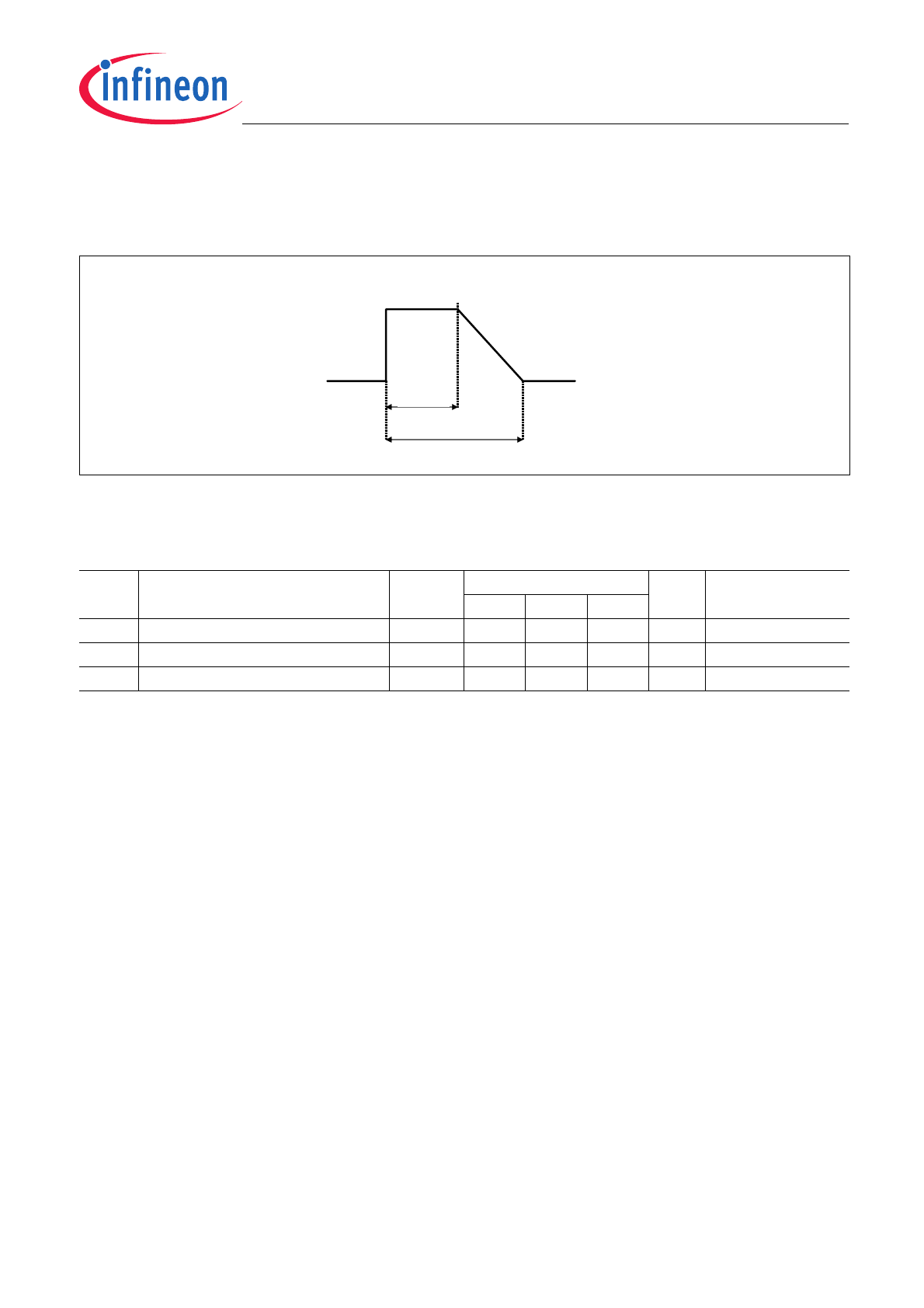
Figure 3
Test Condition
3.2
Thermal Resistance
Pos.
Parameter
Symbol
Limit Values
Unit
Conditions
Min.
Typ.
Max.
3.2.1
–
3.2.2
Junction to Case
1)
1) Not subject to production test, specified by design.
R
thjC
1
K/W
2)
2) Channel 1-6 continously turned on, 0.8W power dissipation per channel
3.2.3
Junction to ambient
1)
R
thjA
15.5
K/W
2)
3)
3) Specified
R
thjA
value is according to Jedec JESD51-2,-5,-7 at natural convection on FR4 2s2p board ; The Product
(Chip+Package) was simulated on a 76.2 x 114.3 x 1.5 mm board with 2 inner copper layers (2 x 70
μm Cu, 2 x 35μm Cu).
Where applicable a thermal via array under the exposed pad contacted the first inner copper layer.
Further informations can be found in Chapter 7.2
12V
40V
10 times
(once/ 30sec)
160ms
350ms
TLE6288R
Description
Data Sheet
10
Rev. 2.5, 2010-10-11
4
Description
4.1
General Functional Description
Channel 1 to 3
•
High Side Configuration with Charge Pump
•
On / off Current Control
•
Peak & Hold Current Control with fixed off time, values adjustable by SPI
•
Type of current control can be selected by SPI
•
Peak Current,Peak Time, Hold Current and Off-Time can be selected by SPI to set average and ripple current
for a given load (refer to
Figure 6
)
Channel 4 to 6
•
Configurable as either High or Low Side switch (by SPI)
•
On / Off operation
4.1.1
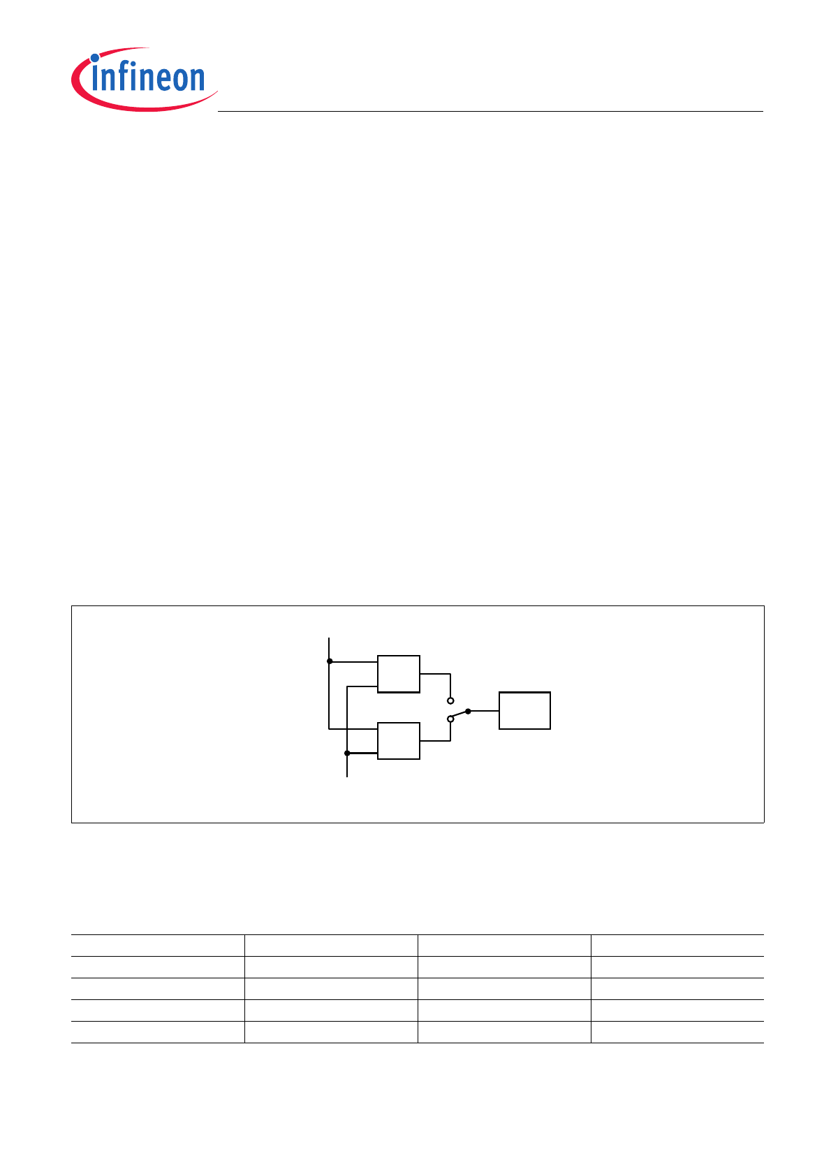
Output Stage Control: Parallel Control and SPI Control
A Boolean operation (either AND or OR) is performed on each of the parallel inputs IN 1 … 6 and respective SPI
data bits, in order to determine the states of the respective outputs. The type of Boolean operation performed is
programmed via the serial interface. Both, parallel inputs and respective SPI databits are high active.
Figure 4
Serial Input Bits 6-11 of Command “Channels on/off”
Each output is independently controlled by an output latch and a common reset line FSIN, which disables all
outputs. A logic high input ‘data bit’ turns the respective output channel ON, a logic low ‘data bit’ turns it OFF.
Table 2
Truth Table
Parallel Input
SPI Bit
Output OR
Output AND
0
0
OFF
OFF
0
1
ON
OFF
1
0
ON
OFF
1
1
ON
ON
OR
AND
Output
Driver
IN 1…6
Serial Input bits 6 -11 of command
„Channels on / off „