

Sense & Control
Datasheet
Rev.1.0, 2010-06-28
TLE4966-2K
High Precision Hall Switch with two Outputs

Edition 2010-06-28
Published by
Infineon Technologies AG
81726 Munich, Germany
©
2010
Infineon Technologies AG
All Rights Reserved.
Legal Disclaimer
The information given in this document shall in no event be regarded as a guarantee of conditions or
characteristics. With respect to any examples or hints given herein, any typical values stated herein and/or any
information regarding the application of the device, Infineon Technologies hereby disclaims any and all warranties
and liabilities of any kind, including without limitation, warranties of non-infringement of intellectual property rights
of any third party.
Information
For further information on technology, delivery terms and conditions and prices, please contact the nearest
Infineon Technologies Office (
www.infineon.com
).
Warnings
Due to technical requirements, components may contain dangerous substances. For information on the types in
question, please contact the nearest Infineon Technologies Office.
Infineon Technologies components may be used in life-support devices or systems only with the express written
approval of Infineon Technologies, if a failure of such components can reasonably be expected to cause the failure
of that life-support device or system or to affect the safety or effectiveness of that device or system. Life support
devices or systems are intended to be implanted in the human body or to support and/or maintain and sustain
and/or protect human life. If they fail, it is reasonable to assume that the health of the user or other persons may
be endangered.

Datasheet
3
Rev.1.0, 2010-06-28
TLE4966-2K
Trademarks of Infineon Technologies AG
ABM™, BlueMoon™, CONVERGATE™, COSIC™, C166™, FALC™, GEMINAX™, GOLDMOS™, ISAC™,
OMNITUNE™, OMNIVIA™, PROSOC™, SEROCCO™, SICOFI™, SIEGET™, SMARTi™, SMINT™,
SOCRATES™, VINAX™, VINETIC™, VOIPRO™, X-GOLD™, XMM™, X-PMU™, XWAY™
Other Trademarks
Microsoft
®
, Visio
®
, Windows
®
, Windows Vista
®
, Visual Studio
®
, Win32
®
of Microsoft Corporation. Linux
®
of
Linus Torvalds. FrameMaker
®
, Adobe
®
Reader™, Adobe Audition
®
of Adobe Systems Incorporated. APOXI
®
,
COMNEON™ of Comneon GmbH & Co. OHG. PrimeCell
®
, RealView
®
, ARM
®
, ARM
®
Developer Suite™ (ADS),
Multi-ICE™, ARM1176JZ-S™, CoreSight™, Embedded Trace Macrocell™ (ETM), Thumb
®
, ETM9™, AMBA™,
ARM7™, ARM9™, ARM7TDMI-S™, ARM926EJ-S™ of ARM Limited. OakDSPCore
®
, TeakLite
®
DSP Core,
OCEM
®
of ParthusCeva Inc. IndoorGPS™, GL-20000™, GL-LN-22™ of Global Locate. mipi™ of MIPI Alliance.
CAT-iq™ of DECT Forum. MIPS™, MIPS II™, 24KEc™, MIPS32
®
, 24KEc™ of MIPS Technologies, Inc. Texas
Instruments
®
, PowerPAD™, C62x™, C55x™, VLYNQ™, Telogy Software™, TMS320C62x™, Code Composer
Studio™, SSI™ of Texas Instruments Incorporated. Bluetooth
®
of Bluetooth SIG, Inc. IrDA
®
of the Infrared Data
Association. Java™, SunOS™, Solaris™ of Sun Microsystems, Inc. Philips
®
, I2C-Bus
®
of Koninklijke Philips
Electronics N.V. Epson
®
of Seiko Epson Corporation. Seiko
®
of Kabushiki Kaisha Hattori Seiko Corporation.
Panasonic
®
of Matsushita Electric Industrial Co., Ltd. Murata
®
of Murata Manufacturing Company. Taiyo Yuden™
of Taiyo Yuden Co., Ltd. TDK
®
of TDK Electronics Company, Ltd. Motorola
®
of Motorola, Inc. National
Semiconductor
®
, MICROWIRE™ of National Semiconductor Corporation. IEEE
®
of The Institute of Electrical and
Electronics Engineers, Inc. Samsung
®
, OneNAND
®
, UtRAM
®
of Samsung Corporation. Toshiba
®
of Toshiba
Corporation. Dallas Semiconductor
®
, 1-Wire
®
of Dallas Semiconductor Corp. ISO
®
of the International
Organization for Standardization. IEC™ of the International Engineering Consortium. EMV™ of EMVCo, LLC.
Zetex
®
of Zetex Semiconductors. Microtec
®
of Microtec Research, Inc. Verilog
®
of Cadence Design Systems, Inc.
ANSI
®
of the American National Standards Institute, Inc. WindRiver
®
and VxWorks
®
of Wind River Systems, Inc.
Nucleus™ of Mentor Graphics Corporation. OmniVision
®
of OmniVision Technologies, Inc. Sharp
®
of Sharp
Corporation. Symbian OS
®
of Symbian Software Ltd. Openwave
®
of Openwave Systems, Inc. Maxim
®
of Maxim
Integrated Products, Inc. Spansion
®
of Spansion LLC. Micron
®
, CellularRAM
®
of Micron Technology, Inc.
RFMD
®
of RF Micro Devices, Inc. EPCOS
®
of EPCOS AG. UNIX
®
of The Open Group. Tektronix
®
of Tektronix,
Inc. Intel
®
of Intel Corporation. Qimonda
®
of Qimonda AG. 1GOneNAND
®
of Samsung Corporation.
HyperTerminal
®
of Hilgraeve, Inc. MATLAB
®
of The MathWorks, Inc. Red Hat
®
of Red Hat, Inc. Palladium
®
of
Cadence Design Systems, Inc. SIRIUS Satellite Radio
®
of SIRIUS Satellite Radio Inc. TOKO
®
of TOKO Inc.
The information in this document is subject to change without notice.
Last Trademarks Update 2008-11-17
Revision History: 2010-06-28, Rev.1.0
Previous Revision:
Page
Subjects (major changes since last revision)

Datasheet
4
Rev.1.0, 2010-06-28
TLE4966-2K
Trademarks of Infineon Technologies AG . . . . . . . . . . . . . . . . . . . . . . 3
1
Overview . . . . . . . . . . . . . . . . . . . . . . . . . . . . . . . . . . . . . . . . . . . . . . . . . . . 5
1.1
Features . . . . . . . . . . . . . . . . . . . . . . . . . . . . . . . . . . . . . . . . . . . . . . . . . . . . 5
1.2
Functional Description . . . . . . . . . . . . . . . . . . . . . . . . . . . . . . . . . . . . . . . . . 5
1.3
Pin Configuration (top view) . . . . . . . . . . . . . . . . . . . . . . . . . . . . . . . . . . . . . 6
2
General . . . . . . . . . . . . . . . . . . . . . . . . . . . . . . . . . . . . . . . . . . . . . . . . . . . . 7
2.1
Block Diagram . . . . . . . . . . . . . . . . . . . . . . . . . . . . . . . . . . . . . . . . . . . . . . . 7
2.2
Circuit Description . . . . . . . . . . . . . . . . . . . . . . . . . . . . . . . . . . . . . . . . . . . . 7
2.3
Application Circuit . . . . . . . . . . . . . . . . . . . . . . . . . . . . . . . . . . . . . . . . . . . . 8
3
Maximum Ratings . . . . . . . . . . . . . . . . . . . . . . . . . . . . . . . . . . . . . . . . . . . 8
4
Operating Range . . . . . . . . . . . . . . . . . . . . . . . . . . . . . . . . . . . . . . . . . . . . 9
5
Electrical and Magnetic Parameters . . . . . . . . . . . . . . . . . . . . . . . . . . . 10
Field Direction Definition . . . . . . . . . . . . . . . . . . . . . . . . . . . . . . . . . . 11
6
Timing Diagrams for the Speed Outputs . . . . . . . . . . . . . . . . . . . . . . . . 11
7
Package Information . . . . . . . . . . . . . . . . . . . . . . . . . . . . . . . . . . . . . . . . 12
7.1
Package Marking . . . . . . . . . . . . . . . . . . . . . . . . . . . . . . . . . . . . . . . . . . . . 12
7.2
Distance between Chip and Package Surface . . . . . . . . . . . . . . . . . . . . . . 12
7.3
Package Outlines . . . . . . . . . . . . . . . . . . . . . . . . . . . . . . . . . . . . . . . . . . . . 12
PCB Footprint for PG-TSOP6-6-5 . . . . . . . . . . . . . . . . . . . . . . . . . . . 13
Product Name
Product Type
Ordering Code
Package
TLE4966-2K
Double Hall Switch
SP000788888
PG-TSOP6-6-5
High Precision Hall Switch with two Outputs
TLE4966-2K
Datasheet
5
Rev.1.0, 2010-06-28
1
Overview
1.1
Features
•
2.7V to 24V supply voltage operation
•
Operation from unregulated power supply
•
High sensitivity and high stability
of the magnetic switching points
•
High resistance to mechanical stress
by Active Error Compensation
•
Reverse battery protection (-18V)
•
Superior temperature stability
•
Peak temperatures up to 195°C
•
Low jitter (typ. 1
μs)
•
Digital output signals
•
Excellent matching of the 2 Hall probes
•
Hall plate distance 1.45mm
•
Two independent speed outputs
•
SMD package PG-TSOP6-6-5
1.2
Functional Description
The TLE4966-2K is an integrated circuit dual Hall-effect sensor designed specifically for highly accurate
applications. Precise magnetic switching points and high temperature stability are achieved by active
compensation circuits and chopper techniques on chip. The sensor provides two independent speed outputs at
Q1 and Q2 with the status (high or low) corresponding to the magnetic field value at the respective Hall element
H1 and H2. Both Hall elements have the identical thresholds for B
OP
and B
RP
(B
OP1
= B
OP2
and B
RP1
= B
RP2
). For
positive magnetic fields (south pole) exceeding the threshold B
OP1
and/or B
OP2
the corresponding output Q1 and/or
Q2 is low, whereas for negative magnetic fields (north pole) lower than B
RP
the output switches to high. Due to the
spatial distance of the two Hall elements on the chip (d = 1.45mm) the two output signals will show a phase
difference in case the sensor is used with a rotating magnetized pole wheel.
Datasheet
6
Rev.1.0, 2010-06-28
TLE4966-2K
Overview
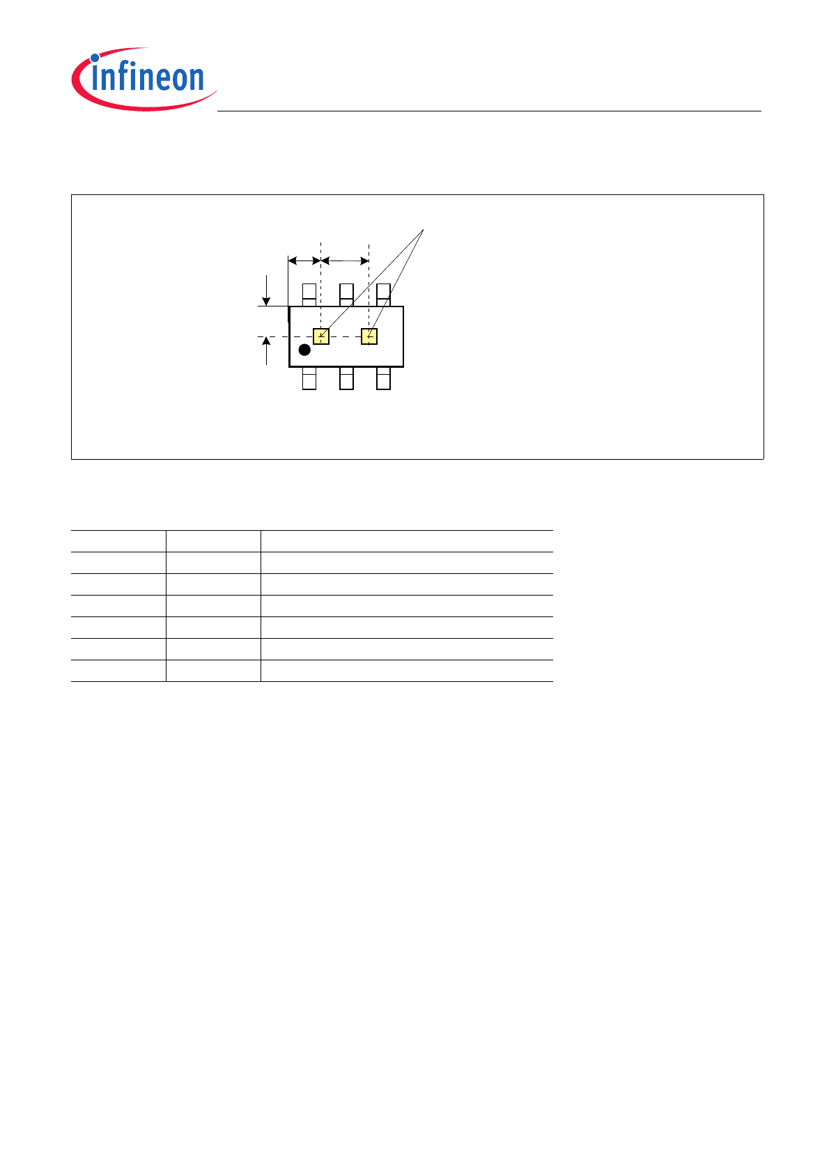
1.3
Pin Configuration (top view)
Figure 1
Pin Definition and Center of Sensitive Area
Table 1
Pin Definitions and Functions
Pin No.
Symbol
Function
1
Q2
Speed 2
2
GND
Recommended connection to GND
3
Q1
Speed 1
4
V
DD
Supply voltage
5
GND
Recommended connection to GND
6
GND
Ground
AEA03645
66
Year (y) = 0...9
Month (m) = 1...9,
O - October
N - November
D - December
s
y
m
1
2
3
4
5
PG-TSOP6-6-5
± 0.15
0.73
± 0.15
0.8
6
1.45
Center of
Sensitive Area
Speed 2
Speed 1
Datasheet
7
Rev.1.0, 2010-06-28
TLE4966-2K
General
2
General
2.1
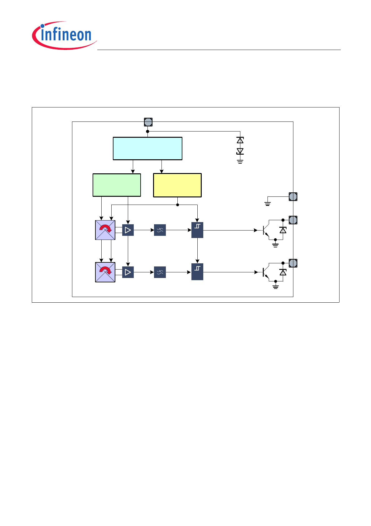
Block Diagram
Figure 2
Block Diagram
2.2
Circuit Description
The chopped Dual Hall Switch comprises two Hall probes, bias generator, compensation circuits, oscillator, and
output transistors.
The bias generator provides currents for the Hall probes and the active circuits. Compensation circuits stabilize the
temperature behavior and reduce influence of technology variations.
The Active Error Compensation rejects offsets in signal stages and the influence of mechanical stress to the Hall
probes caused by molding and soldering processes and other thermal stresses in the package. This chopper
technique together with the threshold generator and the comparator ensures high accurate magnetic switching
thresholds.
Voltage Regulator
(reverse polarity protected)
Oscillator
& Sequencer
Bias and
Compensation
Circuits
Filter
Filter
Amplifier
Amplifier
Chopped
Hall
Probe
ESD
V
DD
Q2
Comparator
with
Hysteresis
Q1
GND
Chopped
Hall
Probe
Datasheet
8
Rev.1.0, 2010-06-28
TLE4966-2K
Maximum Ratings
2.3
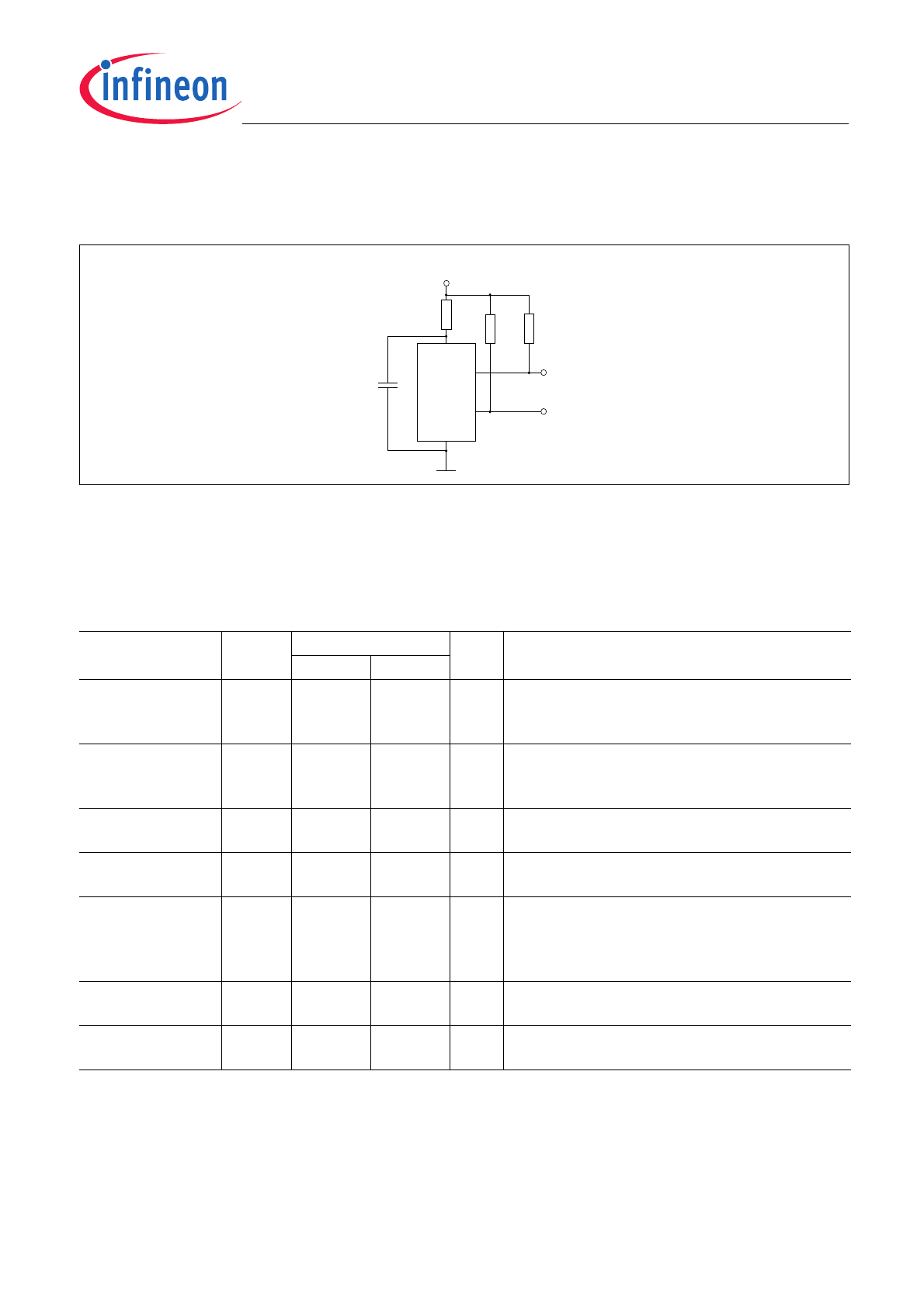
Application Circuit
It is recommended to use a series resistor R
S
with 200
Ω and a capacitor of C
S
= 4.7nF for protection against
overvoltage and transients on the supply line. Pull-up resistors
C
S
Q
1
Q
2
GND
T
L
E
49
66-
2K
V
DD
R
S
R
L
R
L
V
S
R
L
are required for the output pins Q
1
and Q
2
.
Figure 3
Application Circuit
3
Maximum Ratings
Note: Stresses above those listed here may cause permanent damage to the device. Exposure to absolute
maximum rating conditions for extended periods may affect device reliability. Maximum ratings are absolute
ratings; exceeding only one of these values may cause irreversible damage to the integrated circuit.
Table 2
Absolute Maximum Ratings
T
j
= -40°C to 150°C
Parameter
Symbol
Limit Values
Unit
Conditions
min.
max.
Supply voltage
V
DD
V
s
V
s
-18
-18
-18
18
24
26
V
for 1 h,
R
S
≥ 200 Ω
for 5 min,
R
S
≥ 200 Ω
Supply current
through protection
device
I
DD
-50
50
mA
Output voltage
V
Q
-0.7
-0.7
18
26
V
for 5 min @ 1.2 k
Ω pull up
Continuous output
current
I
Q
-50
50
mA
Junction
temperature
T
j
–
–
–
–
155
165
175
195
°C
for 2000 h (not additive)
for 1000 h (not additive)
for 168 h (not additive)
for 3 x 1 h (additive)
Storage
temperature
T
S
-40
150
°C
Magnetic flux
density
B
–
unlimited mT

Table 3
ESD Protection
1)
1) Human Body Model (HBM) tests according to: EOS/ESD Association Standard S5.1-1993 and Mil. Std. 883D method
3015.7
Parameter
Symbol
Limit Values
Unit
Notes
min.
max.
ESD voltage
V
ESD
–
±4
kV
HBM
, R
= 1.5 k
Ω,
C
= 100 pF
T
A
= 25°C
Datasheet
9
Rev.1.0, 2010-06-28
TLE4966-2K
Operating Range
4
Operating Range
The following operating conditions must not be exceeded in order to ensure correct operation of the TLE4966-2K.
All parameters specified in the following sections refer to theses operating conditions unless otherwise mentioned.
Table 4
Operating Range
Parameter
Symbol
Limit Values
Unit
Conditions
min.
typ.
max.
Supply voltage
V
DD
V
S
V
S
2.7
–
–
–
–
–
18
24
26
V
1 h with
R
S
≥ 200 Ω
for 5 min
R
S
≥ 200 Ω
Output voltage
V
Q
-0.7
–
18
V
Junction temperature
T
j
-40
–
–
–
150
175
°C
for 168 h
Output current
I
Q
0
–
10
mA

Datasheet
10
Rev.1.0, 2010-06-28
TLE4966-2K
Electrical and Magnetic Parameters
5
Electrical and Magnetic Parameters
Product characteristics involve the spread of values guaranteed within the specified voltage and temperature
range. Typical characteristics are the median of the production.
Table 5
Electrical Characteristics
1)
1) over operating range, unless otherwise specified. Typical values correspond to
V
DD
= 12 V and
T
A
= 25°C
Parameter
Symbol
Limit Values
Unit
Conditions
min.
typ.
max.
Supply current
I
DD
4
5.2
7
mA
V
DD
= 2.7 V ... 18 V
Reverse current
I
SR
0
0.2
1
mA
V
DD
= -18 V
Output saturation voltage
V
QSAT
–
0.3
0.6
V
I
Q
= 10 mA
Output leakage current
I
QLEAK
–
0.05
10
μA
for
V
Q
= 18 V
Output fall time
t
f
–
0.2
1
μs
R
L
= 1.2 k
Ω;
C
L
< 50 pF
see:
Figure 4
on
Page 11
Output rise time
t
r
–
0.2
1
μs
Chopper frequency
f
OSC
–
320
–
kHz
Switching frequency
f
SW
0
–
15
2)
2) To operate the sensor at the max. switching frequency, the magnetic signal amplitude must be 1.4 times higher than for
static fields. This is due to the -3 dB corner frequency of the low pass filter in the signal path.
kHz
Delay time
3)
3) Systematic delay between magnetic threshold reached and output switching
t
d
–
13
–
μs
Count Signal Delay
t
dc
50
200
1000
ns
Output jitter
4)
4) Jitter is the unpredictable deviation of the output switching delay
t
QJ
–
1
–
μs
RMS
Typ. value for square wave signal 1 kHz
Repeatability of magnetic
thresholds
5)
5)
B
REP
is equivalent to the noise constant
B
REP
–
40
–
μT
RMS
Typ. value for
Δ
B
/
Δ
t
> 12 mT/ms
Power-on time
6)
6) Time from applying
V
DD
≥ 2.7 V to the sensor until the output state is valid
t
PON
–
13
–
μs
V
DD
≥ 2.7 V
Distance of hall plates
d
HALL
–
1.45
–
mm
Thermal resistance
7)
7) Thermal resistance from junction to ambient
Calculation of the ambient temperature (PG-TSOP6-6-5 example)
e.g. for V
DD
= 12.0 V, I
DDtyp
= 5.5 mA, V
QSATtyp
= 0.3 V and 2 x I
Q
= 10 mA
:
Power Dissipation: P
DIS
= 72.0 mW.
In T
A
= T
j
– (R
thJA
× P
DIS
) = 175°C – (100 K / W
× 0.072 W)
Resulting max. ambient temperature: T
A
= 167.8°C
R
thJA
–
100
–
K/W
PG-TSOP6-6-5