

Sense & Control
Datasheet
Rev.1.0, 2010-02-23
TLE4916-1K
Low Power Automotive Hall Switch

Edition 2010-02-23
Published by
Infineon Technologies AG
81726 Munich, Germany
©
2010
Infineon Technologies AG
All Rights Reserved.
Legal Disclaimer
The information given in this document shall in no event be regarded as a guarantee of conditions or
characteristics. With respect to any examples or hints given herein, any typical values stated herein and/or any
information regarding the application of the device, Infineon Technologies hereby disclaims any and all warranties
and liabilities of any kind, including without limitation, warranties of non-infringement of intellectual property rights
of any third party.
Information
For further information on technology, delivery terms and conditions and prices, please contact the nearest
Infineon Technologies Office (
www.infineon.com
).
Warnings
Due to technical requirements, components may contain dangerous substances. For information on the types in
question, please contact the nearest Infineon Technologies Office.
Infineon Technologies components may be used in life-support devices or systems only with the express written
approval of Infineon Technologies, if a failure of such components can reasonably be expected to cause the failure
of that life-support device or system or to affect the safety or effectiveness of that device or system. Life support
devices or systems are intended to be implanted in the human body or to support and/or maintain and sustain
and/or protect human life. If they fail, it is reasonable to assume that the health of the user or other persons may
be endangered.

Datasheet
1
Rev.1.0, 2010-02-23
TLE4916-1K
TLE4916-1K Low-Power Automotive Hall Switch
Revision History: 2010-02-23, Rev.1.0
Previous Version:
Page
Subjects (major changes since last revision)
We Listen to Your Comments
Any information within this document that you feel is wrong, unclear or missing at all?
Your feedback will help us to continuously improve the quality of this document.
Please send your proposal (including a reference to this document) to:
sensors@infineon.com

TLE4916-1K
Table of Contents
Datasheet
2
Rev.1.0, 2010-02-23
1
Product Description 3
1.1
Overview 3
1.2
Features 3
1.3
Target Applications 3
2
Functional Description 4
2.1
General 4
2.2
Pin Configuration (top view) 4
2.3
Pin Description 4
2.4
Block Diagram 5
2.5
Functional Block Description 5
3
Specification 7
3.1
Application Circuit 7
3.2
Absolute Maximum Ratings 8
3.3
Operating Range 8
3.4
Electrical and Magnetic Characteristics 9
4
Package Information 11
4.1
Package Outline SC59 11
4.2
Footprint 12
4.3
Distance between Chip and Package 13
4.4
Package Marking 13
Table of Contents
Product Name
Product Type
Ordering Code
Package
TLE4916-1K
Low Power Hall Switch
SP000649954
PG-SC59-3-4
Low-Power Automotive Hall Switch
TLE4916-1K
TLE4916-1K
Datasheet
3
Rev.1.0, 2010-02-23
1
Product Description
1.1
Overview
The TLE4916-1K is an integrated Hall-Effect Sensor in a SMD package
designed specifically to meet the requirements of low-power automotive
and industrial applications with operating voltages of 2.4V - 5.0V. A
chopped measurement principle provides high stability switching
thresholds for operating temperatures between -40°C and 125°C.
1.2
Features
•
Micro power design
•
2.4V to 5.0V operation
•
High sensitivity and high stability of the magnetic switching points
•
High resistance to mechanical stress by Active Error Compensation
•
High ESD performance (± 4kV HBM)
•
Digital output signal
•
SMD package SC59 (SOT23 compatible)
•
RoHS compliant (Pb free package)
1.3
Target Applications
Target applications for TLE4916-1K are all automotive and industrial applications which require a low-power Hall
switch to save power consumption. Due to its low average supply current of typical 4µA the sensor is ideally suited
for battery powered systems or applications with a stand-by mode.
For example, the Hall switch can be used to provide a wake-up signal for other systems which are in a sleep mode
by detecting a change in the magnetic field, thus reducing overall current consumption.
TLE4916-1K
Functional Description
Datasheet
4
Rev.1.0, 2010-02-23
2
Functional Description
2.1
General
The Low Power Hall IC Switch is comprised of a Hall probe, bias generator, compensation circuits, oscillator,
output latch and a n-channel open drain output transistor.
The bias generator provides currents for the Hall probe and the active circuits. Compensation circuits stabilize the
temperature behavior and reduce influence of technology variations.
The Active Error Compensation rejects offsets in signal stages and the influence of mechanical stress to the Hall
probe caused by molding and soldering processes and other thermal stresses in the package. This chopper
technique together with the threshold generator and the comparator ensure highly accurate magnetic switching
points.
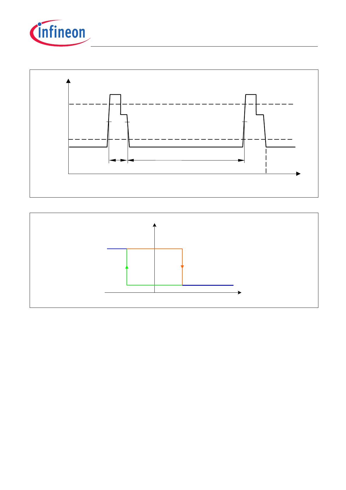
Very low power consumption is achieved with a timing scheme controlled by an oscillator and a sequencer. This
circuitry activates the sensor for 50µs (typical operating time) sets the output state after sequential questioning of
the switch points and latches it with the beginning of the following standby phase (max. 120ms). In the standby
phase the average current is typically reduced to 3.5µA. Because of the long standby time compared to the
operating time the overall averaged current is only slightly higher than the standby current. The output transistor
can sink up to 1 mA with a maximal saturation voltage
V
QSAT
2.2
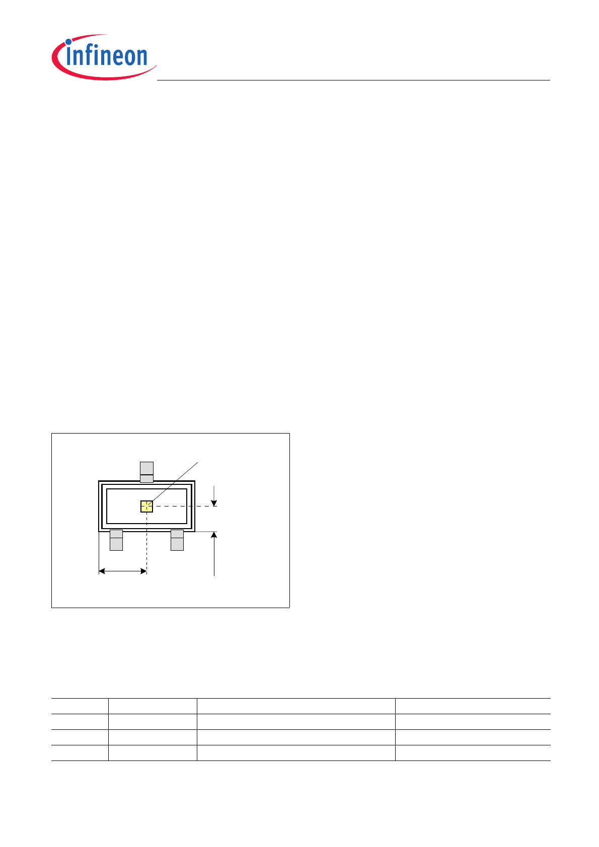
Pin Configuration (top view)
Figure 1
Pin Configuration and Center of Sensitive Area
2.3
Pin Description
Table 1
Pin Description
Pin No.
Symbol
Function
Comment
1
V
S
Supply voltage
2
Q
Output
3
GND
Ground
Center of
Sensitive Area
1
± 0.15
1.5
± 0.15
0.8
2
3
SC59
Datasheet
5
Rev.1.0, 2010-02-23
TLE4916-1K
Functional Description
2.4
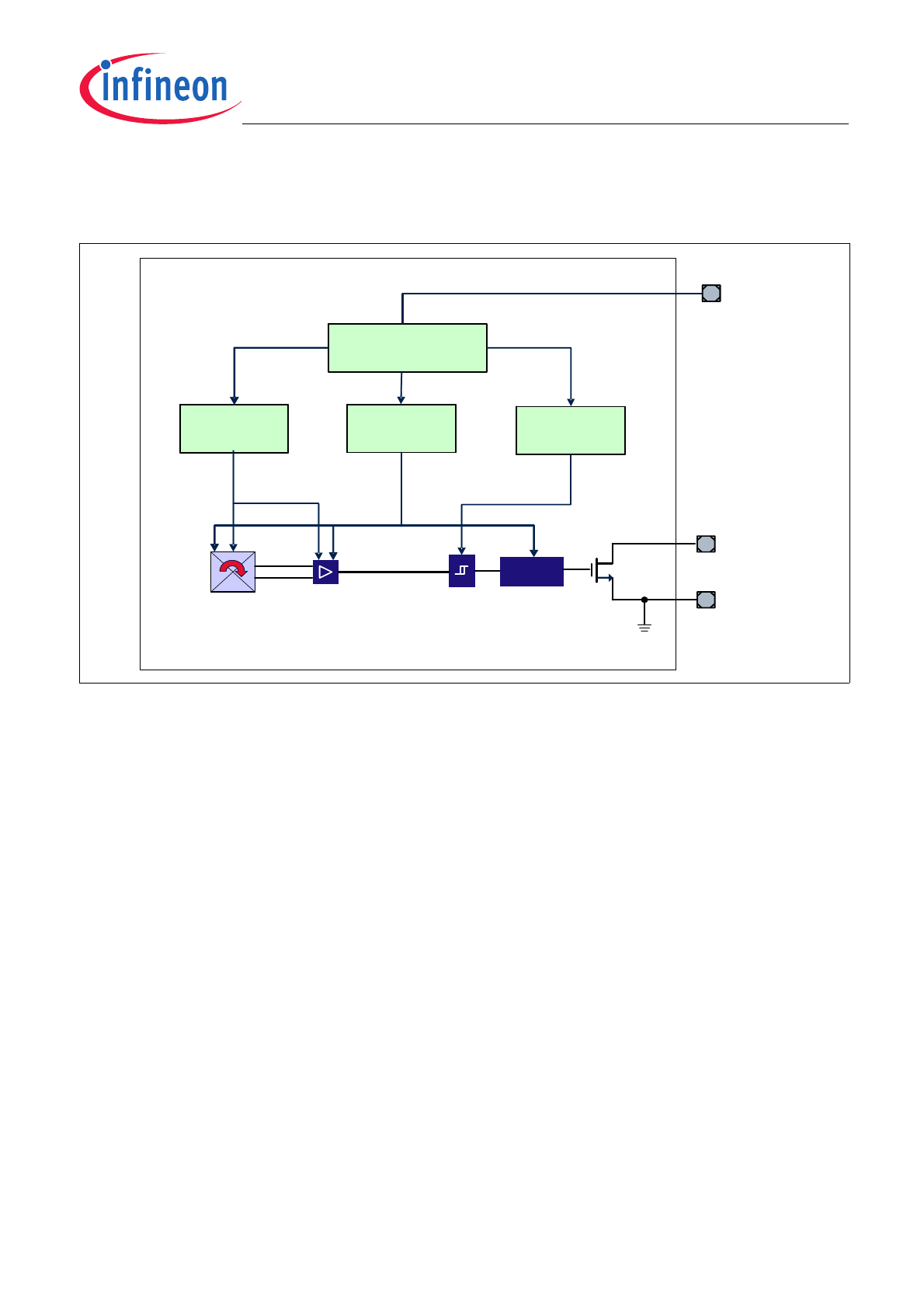
Block Diagram
Figure 2
Functional Block Diagram
2.5
Functional Block Description
The TLE4916-1K is an integrated Hall-Effect Sensor designed specifically to meet the requirements of low-power
applications with operating voltages of 2.4V - 5.0V.
Precise magnetic switching points and high temperature stability are achieved through the unique design of the
internal circuit.
An onboard clock scheme is used to reduce the average operating current of the IC.
During the operating phase the IC compares the actual magnetic field detected to the internally compensated
switching points. The output Q is switched at the end of each operating phase.
During the stand-by phase the output stage is latched and the current consumption of the device reduced to 4µA
µA (typ. value).
The IC switching behaviour is designed as a latch, i.e. it can be switched on (Q = LO) with the south pole of a
magnet and switched off (Q = HI) with the north pole.
.
Bias and Compensation
Circuits
Oscillator
and
Sequencer
Oscillator
and
Sequencer
Chopped
Hall Probe
V
S
V
S
Q
GND
Amplifier
Comparator
with
Hysteresis
Active Error
Compensation
Active Error
Compensation
Active Error
Compensation
Active Error
Compensation
Threshold
Generator
Threshold
Generator
Logic
TLE4916-1K
Functional Description
Datasheet
6
Rev.1.0, 2010-02-23
Figure 3
Timing Diagram
Figure 4
Output Signal
I
S
t
I
SAVG
I
SSTB
Operating
Time
Standby Time
Latch
Output
t
o p
50
μ
s
t
stb
70ms
I
SOPAVG
V
Q
B
op
B
rp
0
B
Datasheet
7
Rev.1.0, 2010-02-23
TLE4916-1K
Specification
3
Specification
3.1
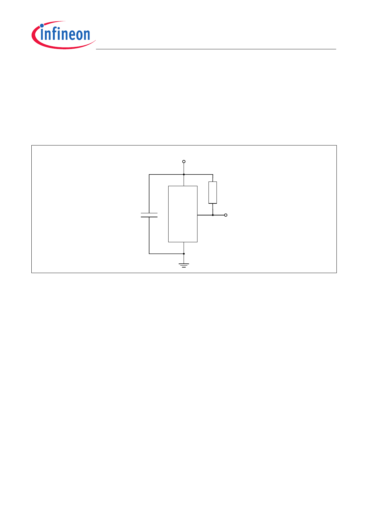
Application Circuit
For operating the sensor a pull-up resistor is required. A ceramic bypass capacitor at Vs to GND is recommended.
Note: The size of the pull-up resistor increases the overall current consumption as additional current is flowing
through this resistor.
Figure 5
Application Circuit
T
L
E
4
91
6-
1K
GND
Q
Vs
R
Q
= 5k
Ω
C
S
= 100nF
TLE4916-1K
Specification
Datasheet
8
Rev.1.0, 2010-02-23
3.2
Absolute Maximum Ratings
Attention: Stresses above the max. values listed here may cause permanent damage to the device.
Exposure to absolute maximum rating conditions for extended periods may affect device
reliability. Maximum ratings are absolute ratings; exceeding only one of these values may
cause irreversible damage to the integrated circuit.
3.3
Operating Range
The following operating conditions must not be exceeded in order to ensure correct operation of the TLE4916-1K.
All parameters specified in the following sections refer to these operating conditions unless otherwise mentioned.
Table 2
Absolute Maximum Rating Parameters
Parameter
Symbol
Limit Values
Unit
Note / Test Condition
Min.
Max.
Supply voltage
V
S
-0.3
5.5
V
Supply current
I
S
-1
2.5
mA
Output voltage
V
Q
-0.3
5.5
V
Output current
I
Q
-1
2
mA
Junction temperature
T
j
–
–
125
150
195
°C
for 5000h (not additive)
for 2000h (not additive)
for 3 x 1h (additive)
Magnetic flux density
B
–
unlimited mT
Thermal resistance SC59
100
K/W
Table 3
ESD Protection
1)
1) Human Body Model (HBM) tests according to: EOS/ESD Association Standard S5.1-1993 and Mil. Std. 883D method
3015.7
Parameter
Symbol
Limit Values
Unit
Note / Test Condition
Min.
Max.
ESD Voltage
V
ESD
±4
kV
HBM, R = 1.5k
Ω,
C = 100pF
T
A
= 25°C
Table 4
Operating Condition Parameters
Parameter
Symbol
Values
Unit
Note / Test Condition
Min.
Typ.
Max.
Supply voltage
V
S
2.4
2.7
5.0
V
Output voltage
V
Q
-0.3
2.7
5.0
V
Junction temperature
T
j
-40
125
°C