

Sensors
Datasheet
Rev 1.0, 2010-12
TLE4906-3K
High Precision Hall-Effect Switch

Edition 2010-12
Published by
Infineon Technologies AG
81726 Munich, Germany
©
2010
Infineon Technologies AG
All Rights Reserved.
Legal Disclaimer
The information given in this document shall in no event be regarded as a guarantee of conditions or
characteristics. With respect to any examples or hints given herein, any typical values stated herein and/or any
information regarding the application of the device, Infineon Technologies hereby disclaims any and all warranties
and liabilities of any kind, including without limitation, warranties of non-infringement of intellectual property rights
of any third party.
Information
For further information on technology, delivery terms and conditions and prices, please contact the nearest
Infineon Technologies Office (
www.infineon.com
).
Warnings
Due to technical requirements, components may contain dangerous substances. For information on the types in
question, please contact the nearest Infineon Technologies Office.
Infineon Technologies components may be used in life-support devices or systems only with the express written
approval of Infineon Technologies, if a failure of such components can reasonably be expected to cause the failure
of that life-support device or system or to affect the safety or effectiveness of that device or system. Life support
devices or systems are intended to be implanted in the human body or to support and/or maintain and sustain
and/or protect human life. If they fail, it is reasonable to assume that the health of the user or other persons may
be endangered.

Datasheet
1
Rev 1.0, 2010-12
TLE4906-3K
TLE4906-3K High Precision Hall Effect Switch
Revision History: 2010-12, Rev 1.0
Previous Version:
Page
Subjects (major changes since last revision)
We Listen to Your Comments
Any information within this document that you feel is wrong, unclear or missing at all?
Your feedback will help us to continuously improve the quality of this document.
Please send your proposal (including a reference to this document) to:
sensors@infineon.com

TLE4906-3K
Table of Contents
Datasheet
2
Rev 1.0, 2010-12
1
Product Description 3
1.1
Overview 3
1.2
Features 3
1.3
Target Applications 3
2
Functional Description 4
2.1
General 4
2.2
Pin Configuration (top view) 4
2.3
Pin Description 4
2.4
Block Diagram 5
2.5
Functional Block Description 5
2.6
Application circuit 7
3
Specification 8
3.1
Absolute Maximum Ratings 8
3.2
Operating Range 9
3.3
Electrical and Magnetic Characteristics 10
4
Package Information 12
4.1
Package Outline 12
4.2
Distance between Chip and Package 13
4.3
Package Marking 13
Table of Contents
Product Name
Product Type
Ordering Code
Package
TLE4906-3K
Unipolar Hall Switch
SP000868844
SC59
High Precision Hall-Effect Switch
TLE4906-3K
Datasheet
3
Rev 1.0, 2010-12
1
Product Description
1.1
Overview
The TLE4906-3K is a high precision Hall effect switch
with highly accurate switching thresholds for operating
temperatures up to 150°C.
1.2
Features
•
2.7V to 24V supply voltage
•
Operation from unregulated power supply
•
High sensitivity and high stability of the magnetic switching points
•
High resistance to mechanical stress by Active Error Compensation
•
Reverse battery protection (-18V)
•
Superior temperature stability
•
Low jitter (typ. 1µs)
•
High ESD performance (± 4kV HBM)
•
Digital output signal
•
SMD package
SC59
(SOT23 compatible)
1.3
Target Applications
Target applications for TLE4906-3K are all automotive applications which require a high precision Hall switch for
position sensing with a operating temperature range from -40°C to +150°C. The TLE4906-3K is a unipolar Hall
switch which is actuated with the south pole of a magnet. A magnetic field above the threshold B
OP
switches the
output to low (output transistor ON) and a magnetic field below the release point B
RP
back to high (transistor OFF).
Datasheet
4
Rev 1.0, 2010-12
TLE4906-3K
Functional Description
2
Functional Description
2.1
General
The TLE4906-3K is an integrated circuit Hall-effect sensor designed specifically for highly accurate applications.
Precise magnetic switching points and high temperature stability are achieved by active compensation circuits and
chopper techniques on chip.
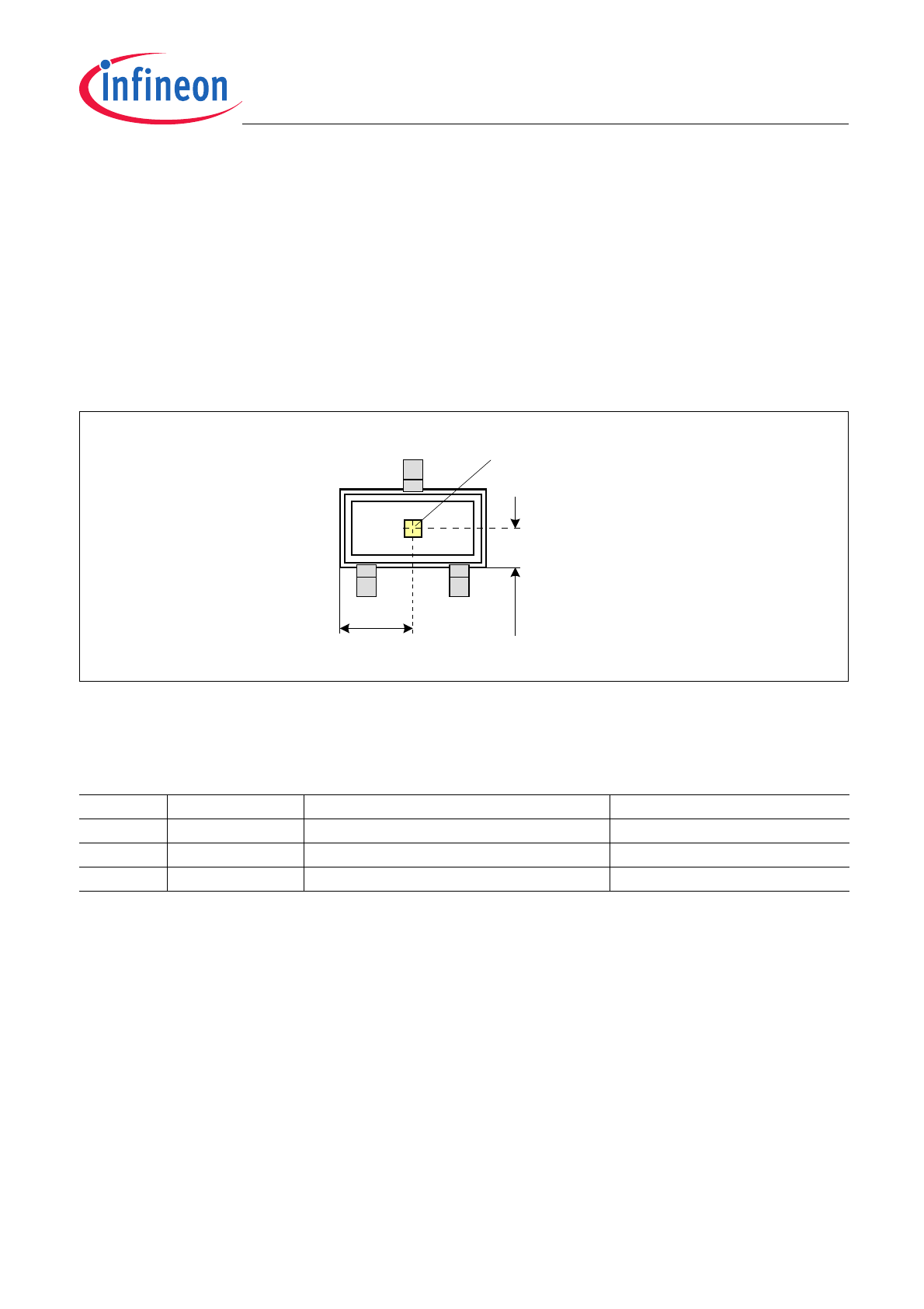
2.2
Pin Configuration (top view)
Figure 1
Pin Configuration and Center of Sensitive Area
2.3
Pin Description
Table 1
Pin Description SC59
Pin No.
Symbol
Function
Comment
1
V
DD
Supply voltage
2
Q
Output
3
GND
Ground
Center of
Sensitive Area
1
± 0.15
1.5
± 0.15
0.8
2
3
SC59
Datasheet
5
Rev 1.0, 2010-12
TLE4906-3K
Functional Description
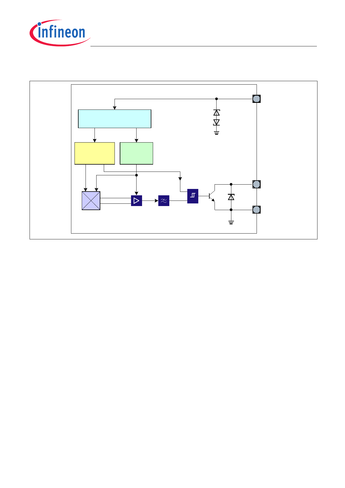
2.4
Block Diagram
Figure 2
Functional Block Diagram
2.5
Functional Block Description
The chopped Hall IC Switch comprises a Hall probe, bias generator, compensation circuits, oscillator and output
transistor.
The bias generator provides currents for the Hall probe and the active circuits. Compensation circuits stabilize the
temperature behavior and reduce technology variations.
The Active Error Compensation rejects offsets in signal stages and the influence of mechanical stress to the Hall
probe caused by molding and soldering processes and other thermal stresses in the package.
This chopper technique together with the threshold generator and the comparator ensure high accurate magnetic
switching points.
Ref
Chopped
Hall Probe
V
DD
Q
GND
Amplifier
Low
Pass
Filter
Comparator
with
Hysteresis
Voltage Regulator
reverse polarity protected
Oscillator
and
Sequencer
Bias and
Compensation
Circuits
Datasheet
6
Rev 1.0, 2010-12
TLE4906-3K
Functional Description
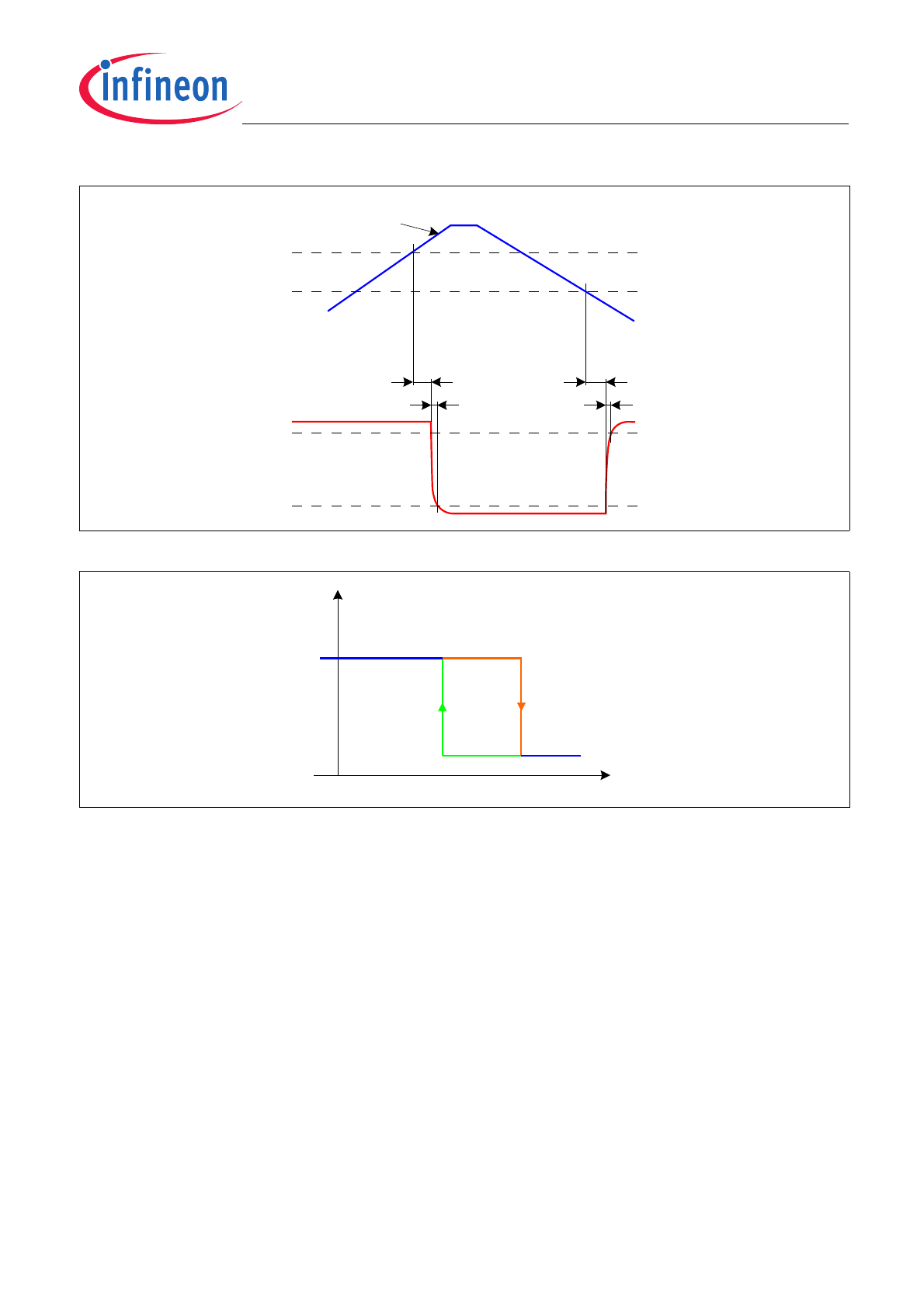
Figure 3
Timing Diagram
Figure 4
Output Signal
Applied
Magnetic
Field
90%
10%
V
Q
t
f
t
d
t
r
t
d
B
OP
B
RP
V
Q
B
op
B
rp
0
B
Datasheet
7
Rev 1.0, 2010-12
TLE4906-3K
Functional Description
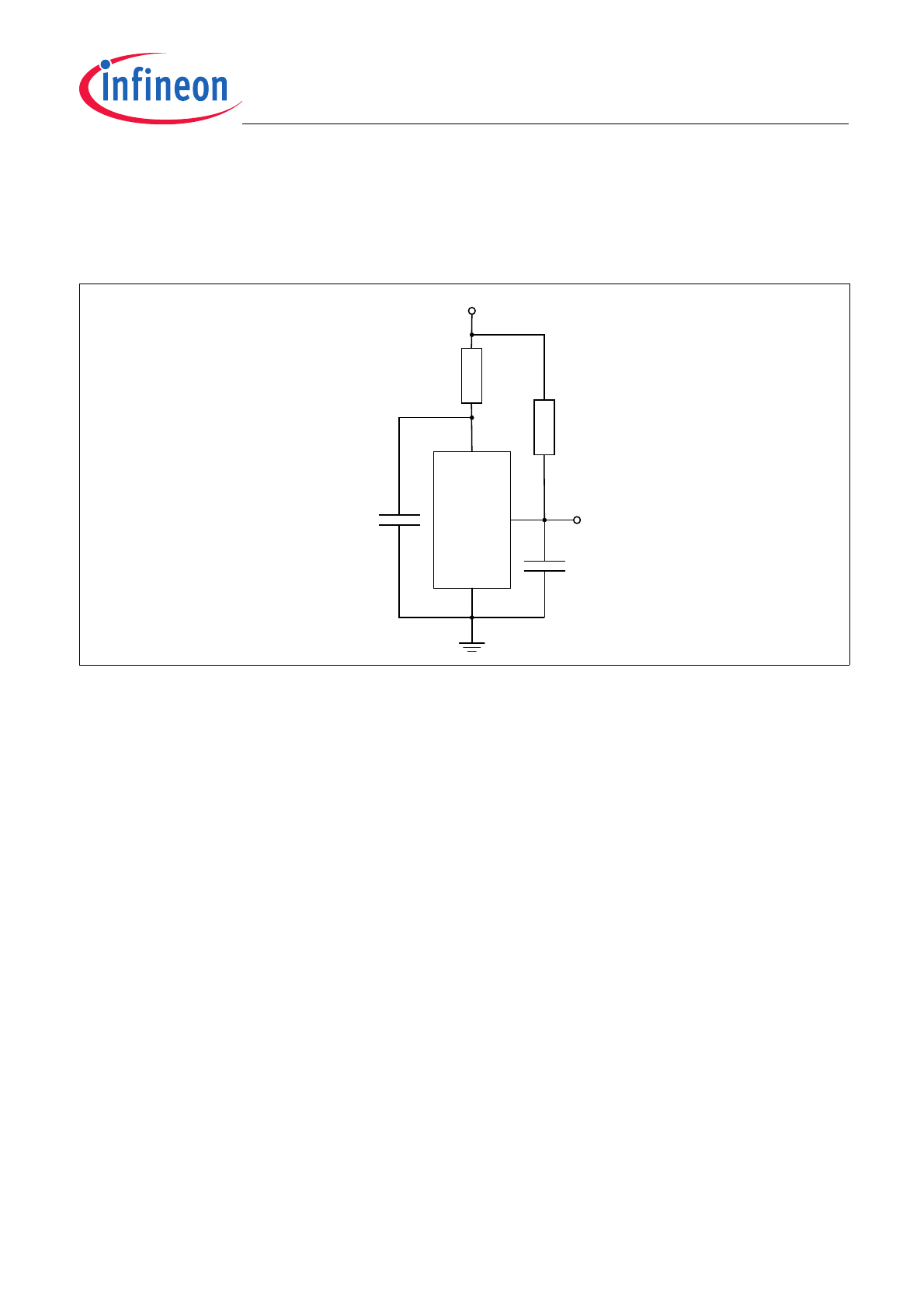
2.6
Application circuit
It is recommended to use a series resistor R
S
with 200
Ω and a capacitor of C
DD
= 4.7nF for protection against
overvoltage and transients on the supply line. A capacitor C
Q
at the Q pin protects the IC from disturbances
coupled to the output. A pull-up resistor R
Q
is also required for the output pin Q.
Figure 5
Application circuit
T
L
E
4906-
3K
GND
Vs
R
Q
= 1.2k
Ω
C
DD
= 4.7nF
R
s
= 200
Ω
V
DD
Q
C
Q
= 4.7nF

Datasheet
8
Rev 1.0, 2010-12
TLE4906-3K
Specification
3
Specification
3.1
Absolute Maximum Ratings
Note: Stresses above the max. values listed here may cause permanent damage to the device. Exposure to
absolute maximum rating conditions for extended periods may affect device reliability. Maximum ratings are
absolute ratings; exceeding only one of these values may cause irreversible damage to the integrated circuit.
Table 2
Absolute Maximum Rating Parameters
T
j
= -40°C to 150°C
Parameter
Symbol
Limit Values
Unit
Note / Test Condition
Min.
Max.
Supply voltage
V
DD
V
S
V
S
-18
-18
-18
18
24
26
V
for 1h, R
S
≥
200
Ω
for 5min, R
S
≥
200
Ω
Supply current through
protection device
I
DD
-50
50
mA
Output voltage
V
Q
-0.7
-0.7
18
26
V
for 5min @ 1.2k
Ω pull up
Continuous output current
I
Q
-50
50
mA
Junction temperature
T
j
–
–
–
–
155
165
175
195
°C
for 2000h (not additive)
for 1000h (not additive)
for 168h (not additive)
for 3 x 1h (additive)
Storage temperature
T
S
-40
150
°C
Magnetic flux density
B
–
unlimited mT
Table 3
ESD Protection
1)
1) Human Body Model (HBM) tests according to: EOS/ESD Association Standard S5.1-1993 and Mil. Std. 883D method
3015.7
Parameter
Symbol
Limit Values
Unit
Note / Test Condition
Min.
Max.
ESD Voltage
V
ESD
±4
kV
HBM, R = 1.5k
Ω,
C = 100pF
T
A
= 25°C