

N e v e r s t o p t h i n k i n g .
Datasheet, Version 2.1, 18 Feb 2005
Power Management & Supply
PFC-DCM IC
Boost Controller
TDA4863/TDA4863G
Power-Factor Controller (PFC)
IC for High Power Factor
and Active Harmonic Filter

Edition 2005-02-18
Published by Infineon Technologies AG,
St.-Martin-Strasse 53,
D-81541 München
©
Infineon Technologies AG 1999.
All Rights Reserved.
Attention please!
The information herein is given to describe certain components and shall not be considered as warranted charac-
teristics.
Terms of delivery and rights to technical change reserved.
We hereby disclaim any and all warranties, including but not limited to warranties of non-infringement, regarding
circuits, descriptions and charts stated herein.
Infineon Technologies is an approved CECC manufacturer.
Information
For further information on technology, delivery terms and conditions and prices please contact your nearest Infi-
neon Technologies Office in Germany or our Infineon Technologies Representatives worldwide (see address list).
Warnings
Due to technical requirements components may contain dangerous substances. For information on the types in
question please contact your nearest Infineon Technologies Office.
Infineon Technologies Components may only be used in life-support devices or systems with the express written
approval of Infineon Technologies, if a failure of such components can reasonably be expected to cause the failure
of that life-support device or system, or to affect the safety or effectiveness of that device or system. Life support
devices or systems are intended to be implanted in the human body, or to support and/or maintain and sustain
and/or protect human life. If they fail, it is reasonable to assume that the health of the user or other persons may
be endangered.
For questions on technology, delivery and prices please contact the Infineon Technologies Offices in Germany or
the Infineon Technologies Companies and Representatives worldwide: see our webpage at http://
www.infineon.com
CoolMOST™, CoolSET™ are trademarks of Infineon Technologies AG.
TDA4863/TDA4863G
Revision History:
2005-02-18
Datasheet
Previous Version: V2.0
Page
Subjects ( major changes since last revision )
Update package information

TDA4863
Table of Contents
Page
Version 2.1
3
2005-02-18
1
Overview . . . . . . . . . . . . . . . . . . . . . . . . . . . . . . . . . . . . . . . . . . . . . . . . . . . 4
1.1
Features . . . . . . . . . . . . . . . . . . . . . . . . . . . . . . . . . . . . . . . . . . . . . . . . . . . . 4
1.2
Improvements Referred to TDA 4862 . . . . . . . . . . . . . . . . . . . . . . . . . . . . . 4
1.3
Description . . . . . . . . . . . . . . . . . . . . . . . . . . . . . . . . . . . . . . . . . . . . . . . . . . 5
1.4
Pin Configuration . . . . . . . . . . . . . . . . . . . . . . . . . . . . . . . . . . . . . . . . . . . . . 6
1.5
Block Diagram . . . . . . . . . . . . . . . . . . . . . . . . . . . . . . . . . . . . . . . . . . . . . . . 8
2
Functional Description . . . . . . . . . . . . . . . . . . . . . . . . . . . . . . . . . . . . . . . 9
2.1
Introduction . . . . . . . . . . . . . . . . . . . . . . . . . . . . . . . . . . . . . . . . . . . . . . . . . 9
2.2
IC Description . . . . . . . . . . . . . . . . . . . . . . . . . . . . . . . . . . . . . . . . . . . . . . . 9
2.3
Voltage Amplifier . . . . . . . . . . . . . . . . . . . . . . . . . . . . . . . . . . . . . . . . . . . . . 9
2.4
Overvoltage Regulator . . . . . . . . . . . . . . . . . . . . . . . . . . . . . . . . . . . . . . . . 10
2.5
Multiplier . . . . . . . . . . . . . . . . . . . . . . . . . . . . . . . . . . . . . . . . . . . . . . . . . . 10
2.6
Current Sense Comparator, LEB and RS Flip-Flop . . . . . . . . . . . . . . . . . . 10
2.7
Zero Current Detector . . . . . . . . . . . . . . . . . . . . . . . . . . . . . . . . . . . . . . . . 10
2.8
Restart Timer . . . . . . . . . . . . . . . . . . . . . . . . . . . . . . . . . . . . . . . . . . . . . . . 11
2.9
Undervoltage Lockout . . . . . . . . . . . . . . . . . . . . . . . . . . . . . . . . . . . . . . . . 11
2.10
Gate Drive . . . . . . . . . . . . . . . . . . . . . . . . . . . . . . . . . . . . . . . . . . . . . . . . . 11
2.11
Signal Diagrams . . . . . . . . . . . . . . . . . . . . . . . . . . . . . . . . . . . . . . . . . . . . 12
3
Electrical Characteristics . . . . . . . . . . . . . . . . . . . . . . . . . . . . . . . . . . . . 13
3.1
Absolute Maximum Ratings . . . . . . . . . . . . . . . . . . . . . . . . . . . . . . . . . . . . 13
3.2
Characteristics . . . . . . . . . . . . . . . . . . . . . . . . . . . . . . . . . . . . . . . . . . . . . . 14
3.3
Electrical Diagrams . . . . . . . . . . . . . . . . . . . . . . . . . . . . . . . . . . . . . . . . . . 17
4
Application Circuit . . . . . . . . . . . . . . . . . . . . . . . . . . . . . . . . . . . . . . . . . . 21
4.1
Results of THD Measurements with Application Board P
out
= 110 W . . . . 22
5
Package Outlines . . . . . . . . . . . . . . . . . . . . . . . . . . . . . . . . . . . . . . . . . . . 25
Version 2.1
4
2005-02-18
Type
Ordering Code
Package
TDA4863
Q67040-S4452
PG-DIP-8-4
TDA4863G
Q67040-A4451
PG-DSO-8-3
Power-Factor Controller (PFC)
IC for High Power Factor
and Active Harmonic Filter
TDA4863
Final Data
Boost Controller
PG-DIP-8-4
PG-DSO-8-3
1
Overview
1.1
Features
• IC for sinusoidal line-current consumption
• Power factor achieves nearly 1
• Controls boost converter as active harmonic
filter for low THD
• Start up with low current consumption
• Zero current detector for discontinuous
operation mode
• Output overvoltage protection
• Output undervoltage lockout
• Internal start up timer
• Totem pole output with active shut down
• Internal leading edge blanking LEB
• Pb-free lead plating; RoHS compliant
1.2
Improvements Referred to TDA 4862
• Suitable for universal input applications with low THD at low load conditions
• Very low start up current
• Accurate OVR and V
ISENSEmax
threshold
• Competition compatible V
CC
thresholds
• Enable threshold referred to V
VSENSE
TDA4863
Overview
Version 2.1
5
2005-02-18
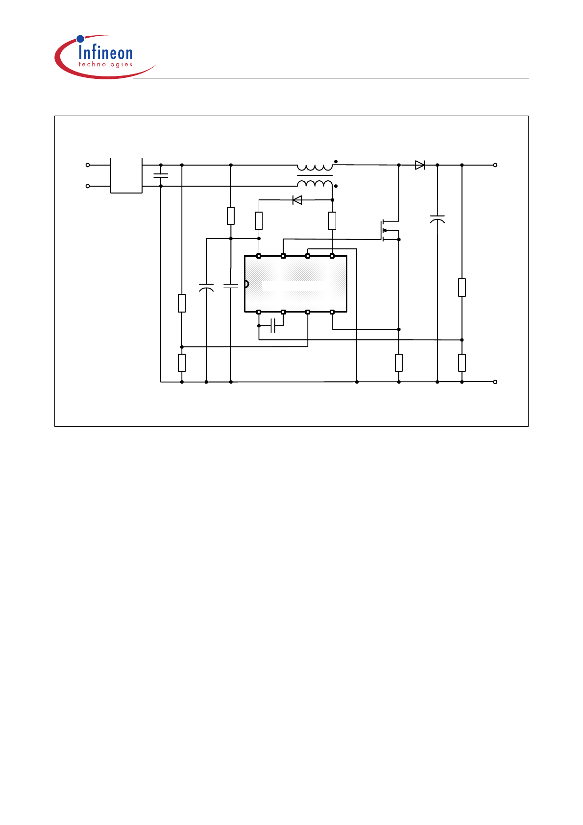
Figure 1
Typical application
1.3
Description
The TDA4863 IC controls a boost converter in a way that sinusoidal current is taken from
the single phase line supply and stabilized DC voltage is available at the output. This
active harmonic filter limits the harmonic currents resulting from the capacitor pulsed
charge currents during rectification. The power factor which decibels the ratio between
active and apparent power is almost one. Line voltage fluctuations can be compensated
very efficiently.
AC line
DC Output
Volage
GND
TDA4863
RF-Filter
and
Rectifier
TDA4863
Overview
Version 2.1
6
2005-02-18
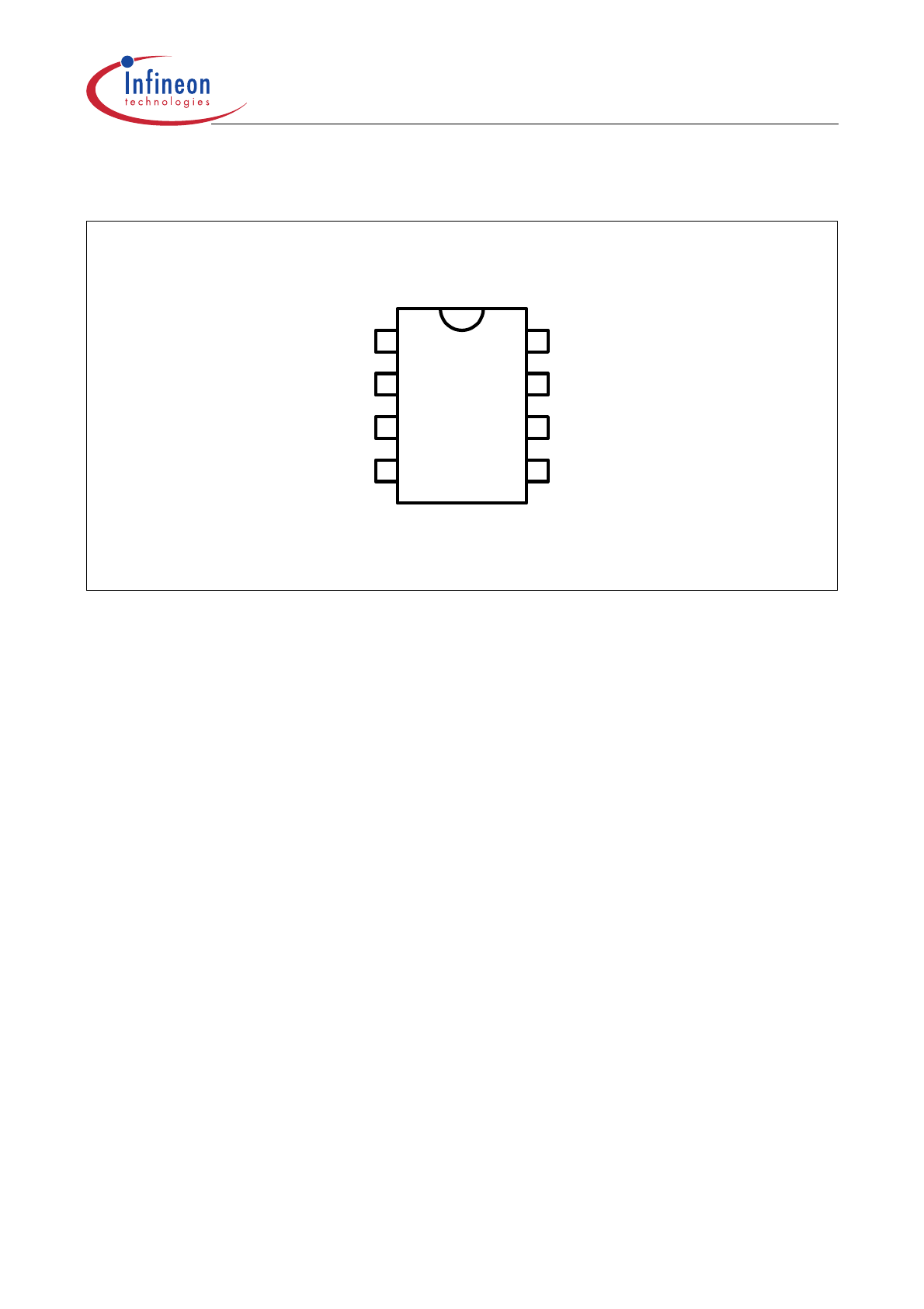
1.4
Pin Configuration
Figure 2
Pin Configuration of TDA4863
1 VSENSE
2 VAOUT
3 MULTIN
4 ISENSE
8 VCC
7 GTDRV
6 GND
5 DETIN

TDA4863
Overview
Version 2.1
7
2005-02-18
Pin Definitions and Functions
Pin
Symbol Description
1
VSENSE Voltage Amplifier Inverting Input
VSENSE is connected via a resistive divider to the boost converter
output. With a capacitor connected to VAOUT the internal error
amplifier acts as an integrator.
2
VAOUT
Voltage Amplifier Output
V
VAOUT
is connected internally to the first multiplier input. To prevent
overshoot the input voltage will be clamped internally at 5 V. Input
voltage less then 2.2 V inhibits the gate driver. If the current flowing
into this pin is exceeding an internal threshold the multiplier output
voltage is reduced to prevent the MOSFET from overvoltage damage.
3
MULTIN Multiplier Input
MULTIN is the second multiplier input and is connected via a resistive
divider to the rectifier output voltage.
4
ISENSE Current Sense Input
ISENSE is connected to a sense resistor controlling the MOSFET
source current. The input is internally clamped at -0.3 V to prevent
negative input voltage interaction. A leading edge blanking circuitry
suppresses voltage spits when turning the MOSFET on.
5
DETIN
Zero Current Detector Input
DETIN is connected to an auxiliary winding monitoring the zero
crossing of the inductor current.
6
GND
Ground
7
GTDRV
Gate Driver Output
GTDRV is the output of a totem-pole circuitry for direct driving a
MOSFET. An active shutdown circuitry ensures that GTDRV is low if
the IC is switched off.
8
VCC
Positive Voltage Supply
If V
CC
exceeds the turn-on threshold the IC is switched on. When V
CC
falls below the turn-off threshold it is switched off and power
consumption is very low. An auxilliary winding is charging a capacitor
which provides the supply current. A second 100 nF ceramic capacitor
should be added to V
CC
to absorb supply current spikes required to
charge the MOSFET gate capacitance.
TDA4863
Overview
Version 2.1
8
2005-02-18
1.5
Block Diagram
Figure 3
Internal Bolck Diagram
GTDRV
Reference
Voltage
Vref
Gate
Drive
+
-
Voltage
Amp
Multiplier
RS
Flip-Flop
+
-
UVLO
Restart
Timer
+
-
Detector
VSENSE
VAOUT
MULTIN
ISENSE
DETIN
VCC
GND
+
-
Current
Comp
multout
+
+
-
-
Inhibit
time delay
2.2V
0.2V
2.5V
uvlo
active
shut down
1.5V
1.0V
12.5V
10V
t
dVA
=2us
t
res
=150us
t
dsd
=70ns
20V
+
1V
Inhibit
Enable
OVR
0.5V
1V
3.5V
Vref
-
+
+
-
Clamp
Current
5V
+
-
5.4V
LEB

TDA4863
Functional Description
Version 2.1
9
2005-02-18
2
Functional Description
2.1
Introduction
Conventional electronic ballasts and switch mode power supplies are designed with a
bridge rectifier and a bulk capacitor. Their disadvantage is that the circuit draws power
from the line when the instantaneous AC voltage exceeds the capacitors voltage. This
occurs near the line voltage peak and causes a high charge current spike with following
characteristics: The apparent power is higher than the real power that means low power
factor condition, the current spikes are non sinusoidal with a high content of harmonics
causing line noise, the rectified voltage depends on load condition and requires a large
bulk capacitor, special efforts in noise suppression are necessary.
With the TDA4863 preconverter a sinusoidal current is achieved which varies in direct
instantaneous proportional to the input voltage half sine wave and so provides a power
factor near 1. This is due to the appearance of almost any complex load like a resistive
one at the AC line. The harmonic distortions are reduced and comply with the IEC555
standard requirements.
2.2
IC Description
The TDA4863 contains a wide bandwidth voltage amplifier used in a feedback loop, an
overvoltage regulator, an one quadrant multiplier with a wide linear operating range, a
current sense comparator, a zero current detector, a PWM and logic circuitry, a totem-
pole MOSFET driver, an internal trimmed voltage reference, a restart timer and an
undervoltage lockout circuitry.
2.3
Voltage Amplifier
With an external capacitor between the pins VSENSE and VAOUT the voltage amplifier
forms an integrator. The integrator monitors the average output voltage over several line
cycles. Typically the integrator´s bandwidth is set below 20 Hz in order to suppress the
100 Hz ripple of the rectified line voltage. The voltage amplifier is internally compensated
and has a gain bandwidth of 5 MHz (typ.) and a phase margin of 80 degrees. The non-
inverting input is biased internally at 2.5 V. The output is directly connected to the
multiplier input.
The gate drive is disabled when VSENSE voltage is less than 0.2 V or VAOUT voltage
is less than 2.2 V.
If the MOSFET is placed nearby the controller switching interferences have to be taken
into account. The output of the voltage amplifier is designed in a way to minimize these
inteferences.

TDA4863
Functional Description
Version 2.1
10
2005-02-18
2.4
Overvoltage Regulator
Because of the integrator´s low bandwidth fast changes of the output voltage can’t be
regulated within an adequate time. Fast output changes occur during initial start-up,
sudden load removal, or output arcing. While the integrator´s differential input voltage
remains zero during this fast changes a peak current is flowing through the external
capacitor into pin VAOUT. If this current exceeds an internal defined margin the
overvoltage regulator circuitry reduces the multiplier output voltage. As a result the on
time of the MOSFET is reduced.
2.5
Multiplier
The one quadrant multiplier regulates the gate driver with respect of the DC output
voltage and the AC half wave rectified input voltage. Both inputs are designed to achieve
good linearity over a wide dynamic range to represent an AC line free from distortion.
Special efforts are made to assure universal line applications with respect to a 90 to
270 V AC range.
The multiplier output is internally clamped at 1.3 V. So the MOSFET is protected against
critical operating during start up.
2.6
Current Sense Comparator, LEB and RS Flip-Flop
An external sense resistor transfers the source current of the MOSFET into a sense
voltage.The multiplier output voltage is compared with this sense voltage.
To protect the current comparator input from negative pulses a current source is inserted
which sends current out of the ISENSE pin every time when V
ISENSE
-signal is falling
below ground potential. The switch-on current peak of the MOSFET is blanked out via a
leading edge blanking circuit with a blanking time of typically 200 ns.
The RS Flip-Flop ensures that only one single switch-on and switch-off pulse appears at
the gate drive output during a given cycle (double pulse suppression).
2.7
Zero Current Detector
The zero current detector senses the inductor current via an auxiliary winding and
ensures that the next on-time of the MOSFET is initiated immediately when the inductor
current has reached zero. This diminishes the reverse recovery losses of the boost
converter diode. The MOSFET is switched off when the voltage drop of the shunt resistor
reaches the voltage level of the multiplier output. So the boost current waveform has a
triangular shape and there are no deadtime gaps between the cycles. This leads to a
continuous AC line current limiting the peak current to twice of the average current.
To prevent false tripping the zero current detector is designed as a Schmitt-Trigger with
a hysteresis of 0.5 V. An internal 5 V clamp protects the input from overvoltage