

ICE1HS01G
Half-Bridge Resonant
Controller
N e v e r s t o p t h i n k i n g .
Power Management & Supply
Datasheet, Version 2.0, 24 August 2009

Edition 24 August 2009
Published by
Infineon Technologies AG
81726 Munich, Germany
© 2007 Infineon Technologies AG
All Rights Reserved.
Legal Disclaimer
The information given in this document shall in no event be regarded as a guarantee of
conditions or characteristics. With respect to any examples or hints given herein, any typical
values stated herein and/or any information regarding the application of the device,
Infineon Technologies hereby disclaims any and all warranties and liabilities of any kind,
including without limitation, warranties of non-infringement of intellectual property rights
of any third party.
Information
For further information on technology, delivery terms and conditions and prices, please
contact the nearest Infineon Technologies Office (
www.infineon.com
).
Warnings
Due to technical requirements, components may contain dangerous substances. For information
on the types in question, please contact the nearest Infineon Technologies Office.
Infineon Technologies components may be used in life-support devices or systems only with
the express written approval of Infineon Technologies, if a failure of such components can
reasonably be expected to cause the failure of that life-support device or system or to affect
the safety or effectiveness of that device or system. Life support devices or systems are
intended to be implanted in the human body or to support and/or maintain and sustain
and/or protect human life. If they fail, it is reasonable to assume that the health of the user
or other persons may be endangered.
For questions on technology, delivery and prices please contact the Infineon Technologies Offices in Germany or
the Infineon Technologies Companies and Representatives worldwide: see our webpage at http://
www.infineon.com
CoolMOS™, CoolSET™ are trademarks of Infineon Technologies AG.
ICE1HS01G
Revision History:
24 August 2009
Target Datasheet
Previous Version:
Page
Subjects (major changes since last revision)
Type
Package
ICE1HS01G
PG-DSO-8
Version 2.0
3
24 August 2009
ICE1HS01G
Half-Bridge Resonant Controller
PG-DSO-8
ICE1HS01G
Product Highlights
• Minimum number of external components
• High accuracy oscillator
• Two-level over current protection
• Over load/open loop protection
• Mains undervoltage protection with adjustable
hysteresis
• Adjustable blanking time for over load protection
and restart
Features
• DSO8 package
• Maximum 600kHz switching frequency
• Adjustable minimum switching frequency with high
accuracy
• 50% duty cycle
• Mains input under votlage protection with adjustable
hysteresis
• Two levels of overcurrent protection: frequency shift
and latch off
• Open-loop/over load protection with extended
blanking time
• Built-in digital and nonlinear softstart
• Adjustable restart time during fault protection period
Applications
• LCD/PDP TV
• AC-DC adapter
• Audio SMPS
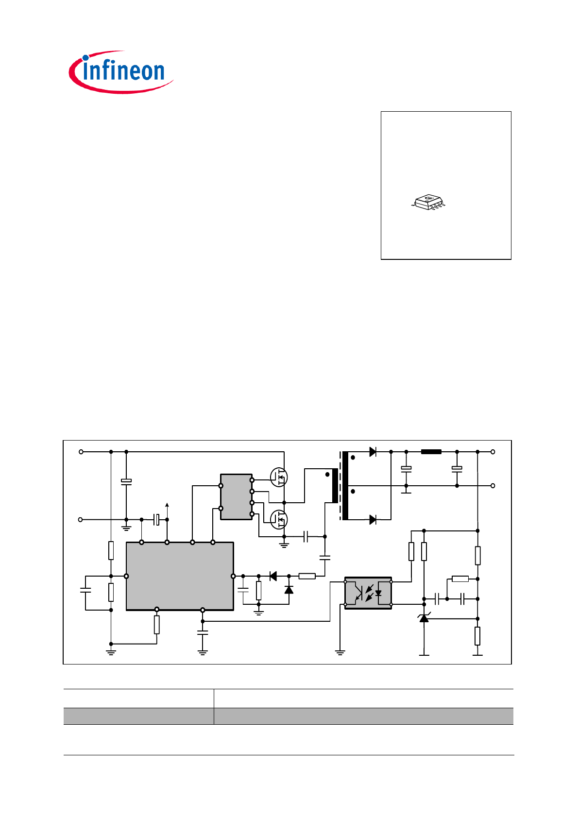
Typical Application Circuit
C
bus
TL431
R
B1
R
B2
R
C1
C
C2
R
OS2
R
OS1
D
O1
D
O2
C
O
C
f
L
f
V
O
V
INDC
W
P
W
SH
W
SL
FMIN
CS
FB
VINS
GND
LG
HG
VCC
ICE1HS01/G
Auxiliary
Supply
Driver
Module
C
C1
R
CS2
R
CS1
D
CS1
D
CS2
C
CS1
C
CS2
C
S
Q
1
Q
2
R
FMIN
R
INS1
R
INS2
C
INS
OPTO
C
FB

Half-Bridge Resonant Controller
ICE1HS01G
Table of Contents
Page
Version 2.0
4
24 August 2009
1
Pin Configuration and Functionality . . . . . . . . . . . . . . . . . . . . . . . . . . . . .5
1.1
Pin configuration with PG-DSO-8 . . . . . . . . . . . . . . . . . . . . . . . . . . . . . . . . .5
1.2
Pin Functionality . . . . . . . . . . . . . . . . . . . . . . . . . . . . . . . . . . . . . . . . . . . . . .5
2
Representative Block Diagram . . . . . . . . . . . . . . . . . . . . . . . . . . . . . . . . . .6
3
Functional description . . . . . . . . . . . . . . . . . . . . . . . . . . . . . . . . . . . . . . . .7
3.1
Oscillator and Pulse Frequency Modulation . . . . . . . . . . . . . . . . . . . . . . . . .7
3.2
IC power supply . . . . . . . . . . . . . . . . . . . . . . . . . . . . . . . . . . . . . . . . . . . . . . .9
3.3
Soft start . . . . . . . . . . . . . . . . . . . . . . . . . . . . . . . . . . . . . . . . . . . . . . . . . . . .9
3.4
Current sense . . . . . . . . . . . . . . . . . . . . . . . . . . . . . . . . . . . . . . . . . . . . . . . .9
3.5
Over current protection . . . . . . . . . . . . . . . . . . . . . . . . . . . . . . . . . . . . . . . .10
3.6
Mains Input Voltage Sense . . . . . . . . . . . . . . . . . . . . . . . . . . . . . . . . . . . . .10
3.7
Over load protection . . . . . . . . . . . . . . . . . . . . . . . . . . . . . . . . . . . . . . . . . . .10
4
Electrical Characteristics . . . . . . . . . . . . . . . . . . . . . . . . . . . . . . . . . . . . .12
4.1
Absolute Maximum Ratings . . . . . . . . . . . . . . . . . . . . . . . . . . . . . . . . . . . . .12
4.2
Operating Range . . . . . . . . . . . . . . . . . . . . . . . . . . . . . . . . . . . . . . . . . . . . .12
4.3
Characteristics . . . . . . . . . . . . . . . . . . . . . . . . . . . . . . . . . . . . . . . . . . . . . . .13
4.3.1
Supply Section . . . . . . . . . . . . . . . . . . . . . . . . . . . . . . . . . . . . . . . . . . . . .13
4.3.2
Oscillator Section . . . . . . . . . . . . . . . . . . . . . . . . . . . . . . . . . . . . . . . . . . .13
4.3.3
Input voltage sense . . . . . . . . . . . . . . . . . . . . . . . . . . . . . . . . . . . . . . . . .14
4.3.4
Current sense . . . . . . . . . . . . . . . . . . . . . . . . . . . . . . . . . . . . . . . . . . . . .14
4.3.5
Soft start . . . . . . . . . . . . . . . . . . . . . . . . . . . . . . . . . . . . . . . . . . . . . . . . .15
4.3.6
Feedback . . . . . . . . . . . . . . . . . . . . . . . . . . . . . . . . . . . . . . . . . . . . . . . . 15
4.3.7
Over load protection . . . . . . . . . . . . . . . . . . . . . . . . . . . . . . . . . . . . . . . . .16
4.3.8
Gate driver . . . . . . . . . . . . . . . . . . . . . . . . . . . . . . . . . . . . . . . . . . . . . . . .16
5
Outline Dimension . . . . . . . . . . . . . . . . . . . . . . . . . . . . . . . . . . . . . . . . . . .17
Version 2.0
5
24 August 2009
Half-Bridge Resonant Controller
ICE1HS01G
Pin Configuration and Functionality
1
Pin Configuration and
Functionality
1.1
Pin configuration with PG-DSO-8
Figure 1
Pin configuration with PG-DSO-8
1.2
Pin Functionality
FMIN (minimum switching frequency)
An external resistor is connected between this pin and
the ground. The voltage of this pin is constant during
operation and thus the resistance determines the
current flowing out of this pin. The minimum switching
frequency is determined by this current. The maximum
switching frequency and the switching frequency
during soft start are also related to the current flowing
out of FMIN pin.
CS(current sense)
The current sense signal is fed to this pin. Inside the IC,
two comparators are provided. If the voltage on CS pin
is higher than the first threshold, IC will increase the
switching frequency to limit the maximum output power
of the converter. If the voltage on this pin exceeds the
second threshold, IC will be latched off immediately.
FB (feedback)
This pin is connected to the collector of the opto-
coupler. Internally, during normal operation, this pin is
connected to reference voltage source with a pull-up
resistor(R
FB
). The IC uses the voltage on this pin to
adjust the switching frequency within the range of
maximum and minimum frequency set by FMIN pin. If
FB voltage is higher than V
FBH
for a certain fixed
blanking time, an extended timer will be started. If over
load/open loop protection exists longer than the
extended blanking time, IC will enter auto-restart mode.
An off timer starts from the instant IC stops switching till
IC starts another soft start. This off time is determined
by the resistors and capacitor connected to VINS pin.
VINS (mains input voltage sense)
The mains input voltage is fed to this pin via a resistive
voltage divider. If the voltage on VINS pin is higher than
the threshold V
INSON
, IC will start to operate with
softstart when VCC increases beyond turn on
threshold. During operation, if the voltage on this pin
falls below the threshold V
INSON
, IC will stop switching
until the voltage on this pin increases again.
When IC goes into over load protection mode, IC will
stop switching and try to restart after a period of time.
This period can be adjusted by connectting different
capacitors between this pin and ground.
GND (ground)
IC common ground.
LG (low side gate drive)
Low side power MOSFET driver.
HG (high-side gate drive)
Up side power MOSFET driver.
VCC (IC power supply)
Supply voltage of the IC.
Pin
Symbol
Function
1
FMIN
Minimum switching frequency
2
CS
Current sense
3
FB
Feedback voltage
4
VINS
Input voltage sense
5
GND
IC ground
6
LG
Low side gate drive
7
HG
High side gate drive
8
VCC
IC power supply
1
2
FMIN
3
4
CS
FB
VINS
8
7
6
5
GND
VCC
HG
LG
Half-Bridge Resonant Controller
ICE1HS01G
Representative Block Diagram
Version 2.0
6
24 August 2009
2
Representative Block Diagram
Figure 2
Representative Block Diagram
HG
LG
VC
C
FM
IN
GN
D
FB
CS
Q
FB
2
00ns
En
A
T
OL
P
20
m
s
I
I
RE
F
2
00ns
C
FB
4
EnA
V
FB
_
B
H
C
FB
1
V
FB
_
O
LP
V
FB
_
L
C
FB
5
EnA
V
FB
_
B
L
C
FB
2
EnA
V
FB
_
C
H
C
FB
3
EnA
V
FB
_
C
L
C
V2
EnA
V
VI
_
H
I
vi
_
h
y
s
C
V3
EnA
V
VI
_
L
V
RE
F
I
VI
_c
h
g
C
V1
EnA
V
VI
N
S
50
0
µs
50
µs
T
VI
_R
Ga
te
D
ri
v
e
r
UV
LO
12
V
11V
Vo
lt
a
g
e
Ref
e
re
nce
Ga
te
D
ri
v
e
r
C
O1
V
CH
C
O2
V
CL
I
DT
C
FS
cl
k
Q
Q
D
V
RE
F
R
FB
VI
N
S
&
G
FB
1
&
G
FB
2
&
G
V3
&
G
V2
Cur
re
n
t
Li
m
ita
tio
n
5.
0
*
I
ch
g_
m
in
V
RE
F
&
G
V1
&
G
LG
&
G
HG
cl
k
St
a
tus
EnA
&
G
V4
5V
1
G
AR
&
G
L
V
CS
_
La
C
CS1
C
CS2
C
CS3
V
CS
_
H
V
CS
_
L
T
CS_
L
a
V
RE
F
I
CS
C
C
CS
I
CS
D
&
G
O1
&
G
O2
C
CS
5
EnA
V
CS
_
C
L
C
CS5
EnA
V
CS_
C
H
So
ft
S
ta
rt
Ena
b
le
SS
End
I
RE
F
I
SS
cl
k
OL
P
UP
Re
set
cl
k
Up
/d
o
w
n
I
OCP
I
RE
F
1
G
CS
2
C
F1
V
FM
IN
Q
F1
V
RE
F
R
S
F
FB
2
Q
S
R
F
FB
1
Q
R
S
F
FB
3
Q
S
R
F
FB
4
Q
S
R
F
VI
_
2
Q
Q
S
R
F
La
tc
h
Q
R
S
F
O1
Q
R
S
F
O2
Q
R
S
F
O3
Q
S
R
F
CS_
1
Q
Q
R
S
F
VI
_1
Q
Q
T
OL
P
_
R
&
G
V5
O
v
e
r C
u
rr
e
n
t Pr
ot
e
ct
ion
(
P
a
te
n
t Pe
n
d
in
g
)
Version 2.0
7
24 August 2009
Half-Bridge Resonant Controller
ICE1HS01G
Functional description
3
Functional description
The controller ICE1HS01G with two gate outputs is
specially designed for LLC resonant half-bridge
converters. An oscillator with accurately-programmed
frequency range is built inside the IC. The two gate
signals are obtained by passing the signal out from the
oscillator through a divide-by-two flip-flop. Therefore,
two signals are of exactly 50% duty cycle and 180
o
out
of phase. To guarantee the zero-voltage-switching and
safe operation in half-bridge topologies, a fixed dead
time of 380ns is inserted in each internal when one
switch is turned off and the other is turned on.
For LLC resonant half-bridge converter, the output
voltage is regulated by changing the switching
frequency. ICE1HS01G offers the designer to choose
suitable operation frequency range by programming
the oscillator with one single resistor.
In addition, ICE1HS01G offers a programmed soft-start
function to limit both the inrush current and the
overshoot in output voltage.
To protect the system during operation, mains input
under-voltage protection and over-current protection
are integrated in ICE1HS01G as well.
3.1
Oscillator and Pulse Frequency
Modulation
The oscillator is programmed with only one external
resistor R
FMIN
connected to FMIN pin. The trimmed
capacitor C
FS
is built inside the IC with high accuracy.
The simplified oscillator circuit is shown in Figure 3.
Figure 3
Simiplified oscillator circuit
The charge current I
chg
is sum of four currents which
are I
chg_min
, I
FB
, I
CS
and I
SS
.
[1]
Everytime the capacitor C
FS
is charged by I
chg
to V
CH
,
the upper switch is turned off and C
FS
will be
discharged through I
disc
. The charge time determines
the on time for gate signal. The discharge time
determines the dead time during transition from one
gate off to another gate on. The switching waveforms
of the oscillator and gate signals are shown in Figure 4.
Figure 4
Oscillator waveforms
According to Figures 3 and 4, the on time of each gate
can be obtained as
[2]
The switching frequency can be obtained as
[3]
where the dead time T
d
is fixed as 380ns.
3.1.1
Minimum charge current
The voltage on pin FMIN is a constant of 1.5V during
normal operation. The resistor R
FMIN
determines the
current(I
FMIN
) flowing out from FMIN pin. Around one-
tenth of I
FMIN
is defined as the minimum charging
current(I
chg_min
), which in turn defines the minimum
switching frequency as follows.
C
O2
C
O1
V
CH
V
CL
R
S
Q
R
S
Q
FMIN
C
F1
Vdd
Q
F1
I
chg_min
C
FS
I
disc
1.5V
R
FMIN
Q
F2
Q
F3
I
chg
I
FB
I
CS
I
SS
FB
CS
ICE1HS01G
I
chg
I
chgmin
I
FB
I
cs
I
ss
+
+
+
=
V
CF
V
delay
V
LG
V
HG
4V
1V
5V
10V
10V
0V
0V
0V
t
t
t
t
t
d
T
on
3C
FS
I
chg
------------
=
f
s
1
2
3C
FS
I
chg
------------ T
d
+
---------------------------------
=
Version 2.0
8
24 August 2009
Half-Bridge Resonant Controller
ICE1HS01G
Functional description
Figure 5
FMIN versus R
FMIN
3.1.2
Feedback regulation
The output information is fed into the controller through
feedback voltage. If the output power is higher, the
feedback voltage will be higher, which will cause the
switching frequency to decrease and vice versa.
The regulation of switching frequency is achieved by
changing the charging current. An accurate operational
transconductance amplifier (OTA) is used to translate
the feedback voltage V
FB
into current I
FB
. The effective
range of feedback voltage is from 0.9V to 3.9V.
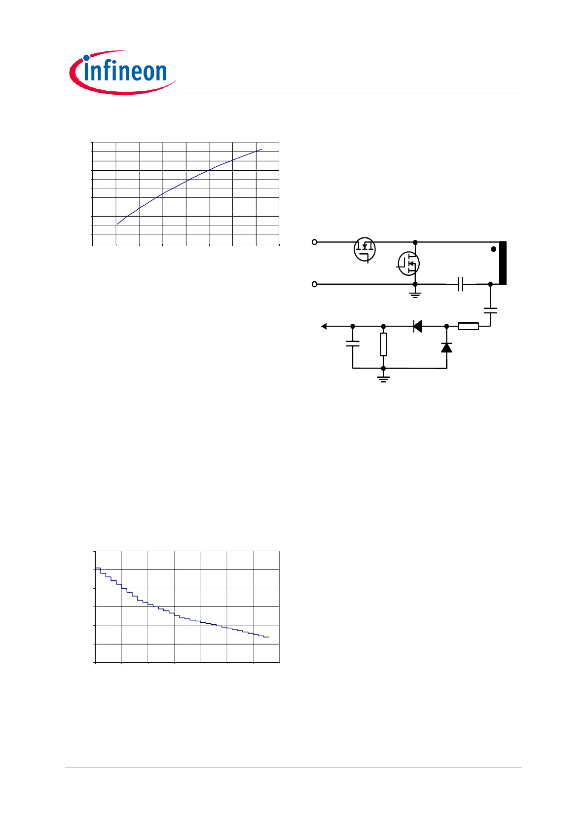
Figure 6 graphs the relationship between the actual
switching frequency and feedback voltage V
FB
when
R
FMIN
=22kohm.
Figure 6
Switching frequency versus V
FB
Burst mode operation is also provided by ICE1HS01G.
During LLC operation, the feedback signal V
FB
is
continuously monitored. When V
FB
drops below V
FB_off
, the switching signal will be disabled after a fixed
blanking time T
FB
. V
FB
will then rise as V
out
starts to
decrease due to no switching signal. Once V
FB
exceeds
the threshold V
FB_on
, the IC resumes to normal
operation.
3.1.3
Current sense current I
CS
In LLC resonant topologies, it is necessary to limit the
resonant current in case of short circuit or other fault
conditions. It is achieved by adding another current Ics
to the charging current I
chg
. I
CS
is limited to 3 times of
the minimum charge current.
3.1.4
Soft start current I
SS
To limit the inrush current and output overshoot during
start up, the switching frequency shall be necessary
high at start up. The switching frequency will change
gradually toward the minimum switching frequency
until the feedback voltage comes into regulation. The
switching frequency will then go to desired value
according to load and input conditions. The soft start
current I
ss
also has a upper limit of around 3.4 times of
minimum charge current. Details of soft start will be
shown later.
3.1.5
Charge current I
chg
The charge current I
chg
for IC oscillator capacitor C
FS
is
the sum of the four parts including I
chg_min
, I
FB
, I
SS
and
I
CS
. To limit the maximum switching frequency,
maximum value of I
chg
is 5 times of I
chg_min
.
In summary, the maximum charge current during
normal operation is 3I
chg_min
while the maximum charge
current during fault condition or softstart is around
4I
chg_min
and 4.43*I
chg_min
respectively. Figure 7 shows
the maximum switching frequency versus minimum
switching frequency during normal operation.
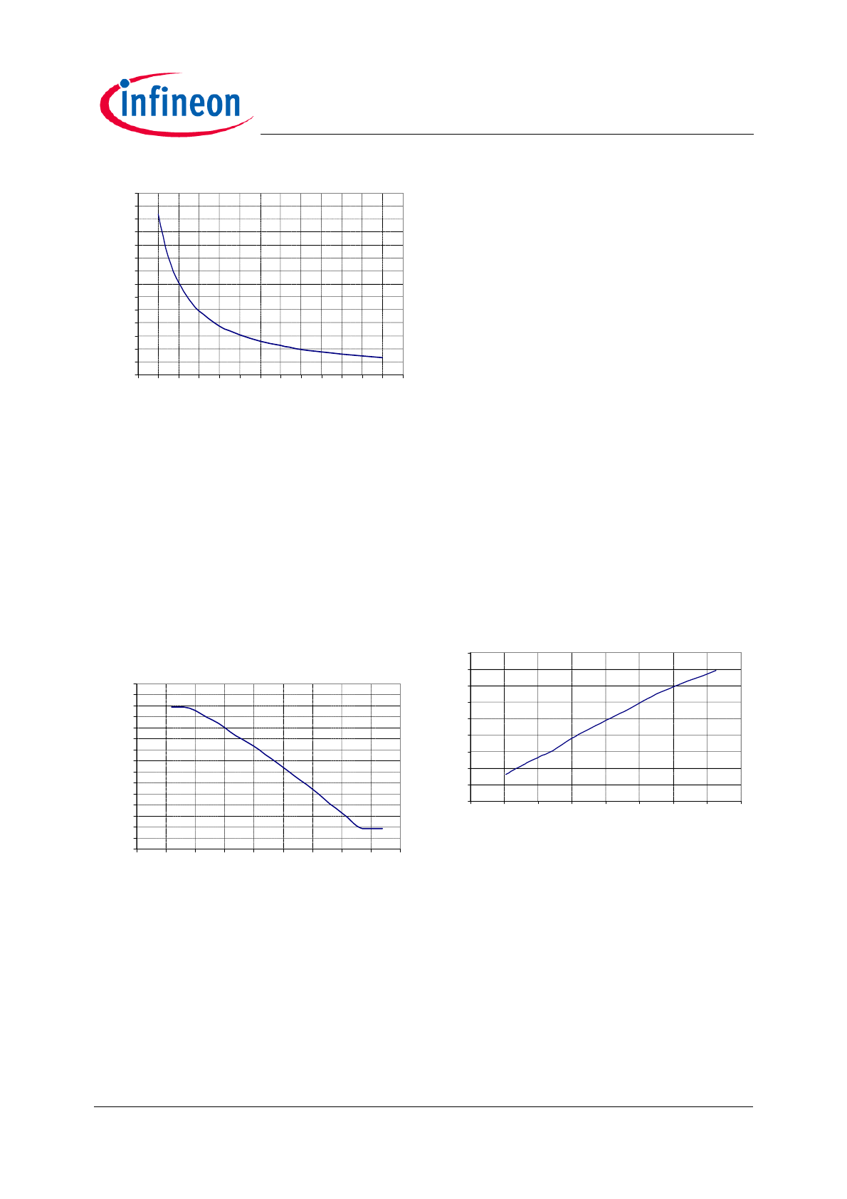
Figure 7
Fmax versus Fmin during normal
operation
0
20
40
60
80
100
120
140
160
180
200
220
240
260
280
0
5 10 15 20 25 30 35 40 45 50 55 60 65
R
FMIN
[kohm]
Mi
ni
m
u
m
s
wi
tc
h
ing
fre
q
uen
cy
[k
H
z]
50
60
70
80
90
100
110
120
130
140
150
160
170
180
190
200
0
0.5
1
1.5
2
2.5
3
3.5
4
4.5
Feedback voltage Vfb [V]
Freq
uency [kHz
]
0
50
100
150
200
250
300
350
400
450
0
25
50
75
100
125
150
175
200
FMIN [kHz]
FM
A
X
[
k
Hz
]
Version 2.0
9
24 August 2009
Half-Bridge Resonant Controller
ICE1HS01G
Functional description
Figure 8 shows the maximum switching frequency
versus minimum switching frequency during softstart.
Figure 8
Fmax_ss versus Fmin during soft start
3.2
IC power supply
The controller ICE1HS01G is targetting at applications
with auxiliary power supply. In most cases, a front-end
PFC pre-regulator with a PFC controller is used in the
same system.
The controller ICE1HS01G starts to operate when the
supply voltage V
VCC
reaches the on-threshold, V
VCCon
of 12V. The minimum operating voltage after turn-on,
V
VCCoff
, is at 11V. The maximum recommended
operating voltage V
VCCmax
is 18V.
3.3
Soft start
At the beginning of the startup phase, the IC provides
a soft start with duration of 32ms with 32 steps. During
this period, the switching frequency is controlled
internally by changing the current I
SS
.
Figure 9 illustrates the actual switching frequency vs
startup time when R
FMIN
=22kohm. During softstart, the
frequency starts from 250kHz, and step by step drops
to normal operation point.
Figure 9
Switching frequency during softstart
when R
FMIN
=22kohm
During soft start, the overload protection is disabled
although FB voltage is high.
3.4
Current sense
Current sense in LLC half bridge converters is for
protection purpose. The voltage of resonant capacitor
C
S
is the sum of the resonant voltage and the dc
voltage which is equal to half of the input bus voltage.
If resonant current is higher, then the voltage on C
S
is
higher.The current informations for both primary side
and secondary side are almost the same and can be
obtained by dividing and filtering the resonant voltage.
The circuit is shown in Figure 10.
Figure 10
Current sense circuit
3.5
Over current protection
The controller ICE1HS01G incorporates two-level over
current protection. In case of over-load condition, the
lower level OCP will be triggerred, the switching
frequency will be increased according to the duration
and power of the over load. The higher level OCP is
used to protect the converter if transformer winding is
shorted, the IC will be latched immediately.
If V
CS
is higher than 0.8V, IC will boost up the switching
frequency. If Vcs is lower than 0.75V, IC will resume to
normal operation gradually. If V
CS
is always higher than
0.8V for 1.5ms, the frequency will rise to its maximum
level. And vice versa.
To sum up, ICE1HS01G will increase the switching
frequency to limit the resonant current in case of
temporary over-load and will also decrease the
switching frequency to its normal value after over-load
condition goes away.
3.6
Mains Input Voltage Sense
The working range of mains input voltage needs to be
specified for LLC resonant converter. It is important for
the controller to have input voltage sensing function
and protection features, which lets the IC stop
switching when the input voltage falls below the
specified range and restarts when the input voltage
increases back within the range. The mains input
voltage sensing circuit is shown Figure 2. With the
0
50
100
150
200
250
300
350
400
450
500
550
0
25
50
75
100
125
150
175
200
FMIN [kHz]
FMA
X
_s
oft sta
rt
[k
Hz
]
0
50
100
150
200
250
300
0
5
10
15
20
25
30
35
Time [ms]
Frequ
ency [kHz]
R
CS2
R
CS1
D
CS1
D
CS2
C
S
Q
1
Q
2
W
P
C
CS1
V
CS
V
BUS
C
CS2
Version 2.0
10
24 August 2009
Half-Bridge Resonant Controller
ICE1HS01G
Functional description
current source I
hys
connected between VINS and
Ground, an adjustable hysteresis between the on and
off input voltage can be created as
[4]
The mains input voltage is divided by R
INS1
and R
INS2
as
shown in the typical application circuit. A current source
I
hys
is connected from VINS pin to ground in the IC. If
the on and off threshold for mains voltage is V
mainon
and
V
mainoff
, the resistors can be decided as
[5]
[6]
3.7
Over load protection
In case of open control loop or output over load fault,
the FB voltage will increase to its maximum level. If FB
voltage is higher than V
FBH
and this condition last
longer than a fixed blanking time of T
OLP
(20ms), the IC
will start the extended blanking timer. The extended
blanking timer is realized by charging and discharging
the filter capacitor C
FB
via the pull up resistor R
FB
and
Q
FB
. The circuit for extended blanking timer is shown in
Figure 11.
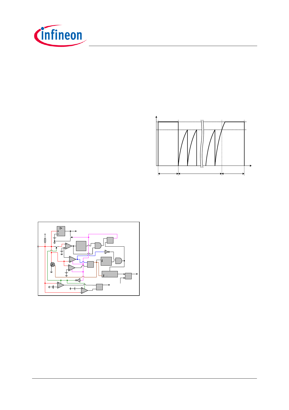
Figure 11
Circuit connected to FB pin
The FB voltage waveform during a OLP period is
shown in Figure 12. After FB voltage has been higher
than V
FBH
for the fixed blanking time t1 shown in Figure
11, IC will use internal switch Q
FB
to discharge V
FB
to
V
FBL
. After the switch Q
FB
is released, C
FB
will be
charged up by Vdd through R
FB
. The time needed for
C
FB
being charged to V
FBH
can be calculated as
[7]
If C
FB
is 10nF, the time is about 439us. After V
FB
reaches V
FBH
, an internal counter will increase by 1 and
the capacitor is discharged to 0.5V by Q
FB
again. The
charging and discharging process of C
FB
will be
repeated for N
OLP_E
times if the fault condition still exist.
After the last time of N
OLP_E
the FB voltage is pulled
down to zero, IC will stop the switch when FB voltage
rises to V
FBH
again. This is called over load/open loop
proteciton. During the charging and discharging period,
the IC will operate with frequency determined by I
chg_min
and I
CS
.
Figure 12
FB voltage waveform during over load
protection
If the converter returns to normal operation during the
extended blanking time period, FB voltage can not
reach V
FBH
again. Therefore, after FB voltage is
discharged to zero voltage, if it can not reach V
FBH
within T
OLP_R
, IC will reset all the fault timer to zero and
return to normal operation.
After IC enters into OLP, both switches will be stopped.
However, the IC remains active and will try to start with
soft start after an adjustable period. This period is
realized by charging and discharging the capacitor C
INS
connected to VINS pin for N
OLP_R
times. The time is
therefore determined by the capacitor C
INS
and resistor
R
INS1
and R
INS2
. The circuit implementation of the
adjustable off time is shown in Figure 13 and Figure 14
shows the voltage waveform of VINS in this case.
As shown in Figure 14, the C
INS
is discharged to V
INS_L
when IC enters into OLP at time t1. After that, an
internal constant current source I
INST
is turned on to
charge C
INS
. Once the voltage on VINS is charged to
V
INS_H
, the current source will be turned off and C
INS
is
discharged by another switch Q3 to V
INS_L
again. The
charging and discharging of C
INS
is thought as one
cycle. The cylce time is also influenced by the bus
V
HYS
R
INS1
I
hys
⋅
=
R
INS1
V
mainon
V
mainoff
–
I
hys
-------------------------------------------
=
R
INS2
R
INS1
V
INSON
V
mainoff
V
INSON
–
-------------------------------------------
⋅
=
FB
I
1.0V
I
FB
Vdd
R
FB
C
FB1
4.5V
T
OLP
24ms
C
FB3
C
FB2
EnA
EnA
0.5V
S
R
Q
Q
FB
CLK
OLP
UP
Reset
T
OLP_R
1.2ms
S
R
Q
C
FB4
EnA
C
FB5
EnA
0.8V
0.5V
S
R Q
Gate_off
AR
I
ref
S
R
Q
AR_R
ICE1HS01G
t
chg
V
dd
V
–
FBH
V
dd
V
FBL
–
---------------------------
ln
–
R
FB
C
FB
⋅
⋅
=
V
FB
(V
)
Time
5V
4.5V
t
1
t
2
t
3
0.5V