

SPIDER - TLE7244SL
8 Channel Protected Low-Side Relay Switch
Datasheet, Rev. 1.3, October 2011
Automotive Power

Datasheet
2
Rev. 1.3, 2011-10-21
SPI Driver for Enhanced Relay Control
SPIDER - TLE7244SL
Table of Contents
1
Overview . . . . . . . . . . . . . . . . . . . . . . . . . . . . . . . . . . . . . . . . . . . . . . . . . . . . . . . . . . . . . . . . . . . . . . . 3
2
Block Diagram . . . . . . . . . . . . . . . . . . . . . . . . . . . . . . . . . . . . . . . . . . . . . . . . . . . . . . . . . . . . . . . . . . . 5
3
Pin Configuration . . . . . . . . . . . . . . . . . . . . . . . . . . . . . . . . . . . . . . . . . . . . . . . . . . . . . . . . . . . . . . . . 6
3.1
Pin Assignment . . . . . . . . . . . . . . . . . . . . . . . . . . . . . . . . . . . . . . . . . . . . . . . . . . . . . . . . . . . . . . . . . . . 6
3.2
Pin Definitions and Functions . . . . . . . . . . . . . . . . . . . . . . . . . . . . . . . . . . . . . . . . . . . . . . . . . . . . . . . . 6
3.3
Voltage and Current naming definition . . . . . . . . . . . . . . . . . . . . . . . . . . . . . . . . . . . . . . . . . . . . . . . . . 8
4
General Product Characteristics . . . . . . . . . . . . . . . . . . . . . . . . . . . . . . . . . . . . . . . . . . . . . . . . . . . . 9
4.1
Absolute Maximum Ratings . . . . . . . . . . . . . . . . . . . . . . . . . . . . . . . . . . . . . . . . . . . . . . . . . . . . . . . . . 9
4.2
Functional Range . . . . . . . . . . . . . . . . . . . . . . . . . . . . . . . . . . . . . . . . . . . . . . . . . . . . . . . . . . . . . . . . 10
4.3
Thermal Resistance . . . . . . . . . . . . . . . . . . . . . . . . . . . . . . . . . . . . . . . . . . . . . . . . . . . . . . . . . . . . . . 10
5
Input and Power Stages . . . . . . . . . . . . . . . . . . . . . . . . . . . . . . . . . . . . . . . . . . . . . . . . . . . . . . . . . . 11
5.1
Power Supply . . . . . . . . . . . . . . . . . . . . . . . . . . . . . . . . . . . . . . . . . . . . . . . . . . . . . . . . . . . . . . . . . . . 11
5.1.1
Limp Home Mode . . . . . . . . . . . . . . . . . . . . . . . . . . . . . . . . . . . . . . . . . . . . . . . . . . . . . . . . . . . . . . 11
5.2
Input Circuit . . . . . . . . . . . . . . . . . . . . . . . . . . . . . . . . . . . . . . . . . . . . . . . . . . . . . . . . . . . . . . . . . . . . . 11
5.2.1
Inductive Output Clamp . . . . . . . . . . . . . . . . . . . . . . . . . . . . . . . . . . . . . . . . . . . . . . . . . . . . . . . . . . 12
5.2.2
Timing Diagrams . . . . . . . . . . . . . . . . . . . . . . . . . . . . . . . . . . . . . . . . . . . . . . . . . . . . . . . . . . . . . . . 13
5.3
Input and Power Stages Characteristics . . . . . . . . . . . . . . . . . . . . . . . . . . . . . . . . . . . . . . . . . . . . . . . 14
6
Protection Functions . . . . . . . . . . . . . . . . . . . . . . . . . . . . . . . . . . . . . . . . . . . . . . . . . . . . . . . . . . . . 16
6.1
Over Load Protection . . . . . . . . . . . . . . . . . . . . . . . . . . . . . . . . . . . . . . . . . . . . . . . . . . . . . . . . . . . . . 16
6.2
Over Temperature Protection . . . . . . . . . . . . . . . . . . . . . . . . . . . . . . . . . . . . . . . . . . . . . . . . . . . . . . . 16
6.3
Reverse Polarity Protection . . . . . . . . . . . . . . . . . . . . . . . . . . . . . . . . . . . . . . . . . . . . . . . . . . . . . . . . 16
6.4
Protection Characteristics . . . . . . . . . . . . . . . . . . . . . . . . . . . . . . . . . . . . . . . . . . . . . . . . . . . . . . . . . . 17
7
Diagnosis Features . . . . . . . . . . . . . . . . . . . . . . . . . . . . . . . . . . . . . . . . . . . . . . . . . . . . . . . . . . . . . . 18
7.1
Diagnosis Characteristics . . . . . . . . . . . . . . . . . . . . . . . . . . . . . . . . . . . . . . . . . . . . . . . . . . . . . . . . . . 18
8
Serial Peripheral Interface (SPI) . . . . . . . . . . . . . . . . . . . . . . . . . . . . . . . . . . . . . . . . . . . . . . . . . . . 19
8.1
SPI Signal Description . . . . . . . . . . . . . . . . . . . . . . . . . . . . . . . . . . . . . . . . . . . . . . . . . . . . . . . . . . . . 19
8.2
Daisy Chain Capability . . . . . . . . . . . . . . . . . . . . . . . . . . . . . . . . . . . . . . . . . . . . . . . . . . . . . . . . . . . . 20
8.3
SPI Protocol . . . . . . . . . . . . . . . . . . . . . . . . . . . . . . . . . . . . . . . . . . . . . . . . . . . . . . . . . . . . . . . . . . . . 21
8.3.1
Timing Diagrams . . . . . . . . . . . . . . . . . . . . . . . . . . . . . . . . . . . . . . . . . . . . . . . . . . . . . . . . . . . . . . . 22
8.4
SPI Characteristics . . . . . . . . . . . . . . . . . . . . . . . . . . . . . . . . . . . . . . . . . . . . . . . . . . . . . . . . . . . . . . . 23
9
Application Information . . . . . . . . . . . . . . . . . . . . . . . . . . . . . . . . . . . . . . . . . . . . . . . . . . . . . . . . . . 25
10
Package Outlines . . . . . . . . . . . . . . . . . . . . . . . . . . . . . . . . . . . . . . . . . . . . . . . . . . . . . . . . . . . . . . . 26
11
Revision History . . . . . . . . . . . . . . . . . . . . . . . . . . . . . . . . . . . . . . . . . . . . . . . . . . . . . . . . . . . . . . . . 27
Table of Contents
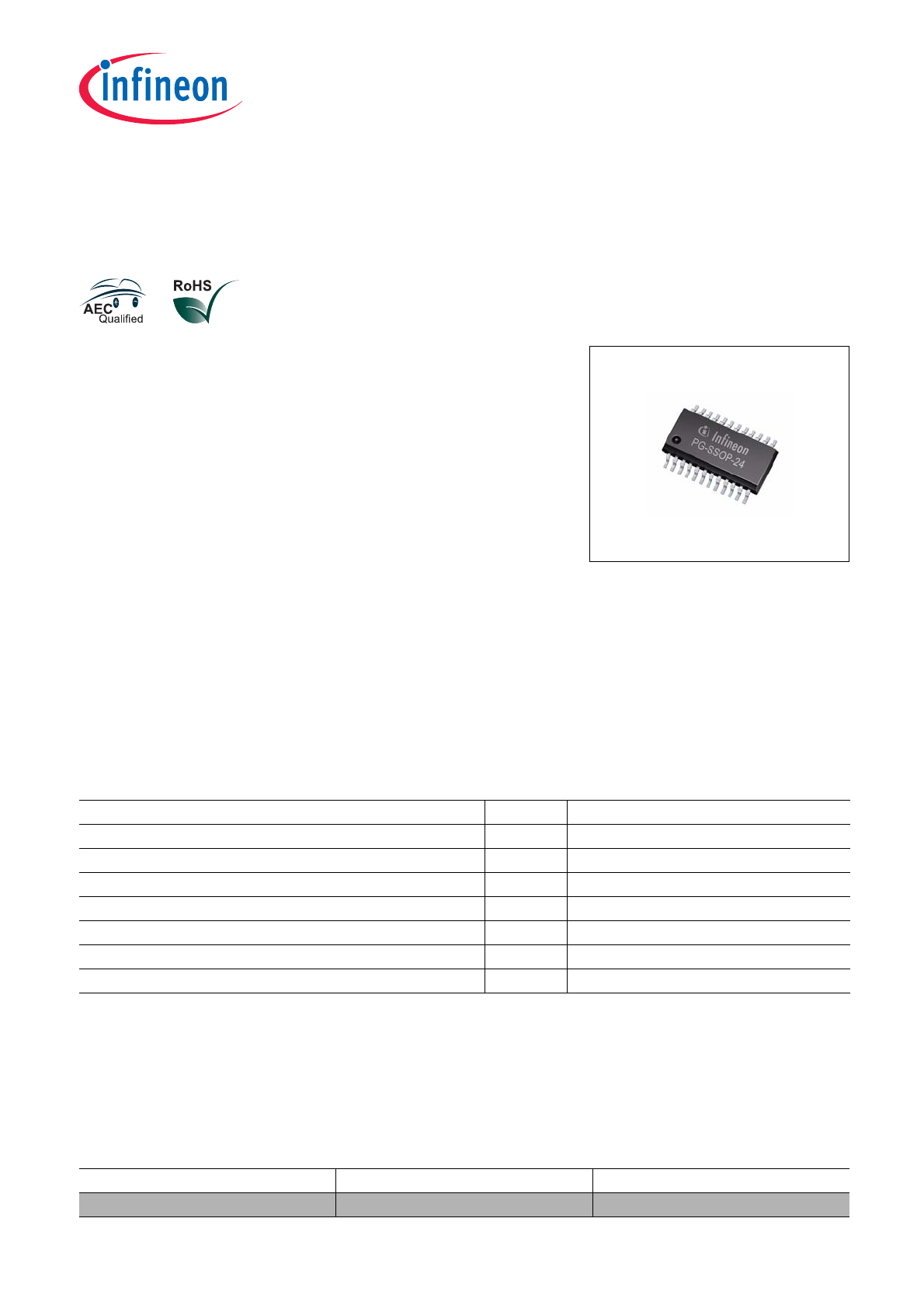
PG-SSOP-24-7
Type
Package
Marking
SPIDER - TLE7244SL
PG-SSOP-24-7
TLE7244SL_A
Datasheet
3
Rev. 1.3, 2011-10-21
SPI Driver for Enhanced Relay Control
SPIDER - TLE7244SL
SPIDER - TLE7244SL
1
Overview
Features
•
4 input pins providing flexible PWM configuration
•
Limp home functionality (direct driving) provided by a dedicated pin
•
16 bit SPI for diagnostics and control
•
Daisy chain capability also compatible with 8bit SPI devices
•
Very wide range of digital supply voltage
•
Green Product (RoHS compliant)
•
AEC Qualified
Description
The SPIDER - TLE7244SL is a eight channel low-side switch in PG-SSOP-24-7 package providing embedded
protective functions.
It is especially designed as relay driver in automotive applications.
A serial peripheral interface (SPI) is utilized for control and diagnosis of the device and the load.
For direct control and PWM there are four input pins available.
The device is monolithically integrated. The power transistors are built by N-channel MOSFETs.
Diagnostic Features
•
latched diagnostic information via SPI register
•
Overtemperature monitoring
•
Overload detection in ON state
•
Open load detection in OFF state
Table 1
Basic Electrical data
Digital supply voltage
V
DD
3.0 V ... 5.5 V
Analog supply voltage
V
DDA
4.5 V ... 5.5 V
Max. ON State resistance at
T
j
= 150°C for each channel
R
DS(ON,max)
1.7
Ω
Nominal load current
I
L (nom)
290 mA
Overload switch off threshold
I
D (OVL,max)
950 mA
Output leakage current per channel at 25 °C
I
D (STB,max)
1 µA
Drain to Source clamping voltage
V
DS(AZ)
41 V
Maximum SPI clock frequency
f
SCLK,max
5 MHz

SPI Driver for Enhanced Relay Control
SPIDER - TLE7244SL
Overview
Datasheet
4
Rev. 1.3, 2011-10-21
Protection Functions
•
Short circuit
•
Over load
•
Over temperature
•
Electrostatic discharge (ESD)
Application
•
All types of resistive, inductive and capacitive loads
•
Especially designed for driving relays in automotive applications
Detailed Description
The SPIDER - TLE7244SL is a eight channel low-side relay switch designed for typical automotive relays
providing embedded protective functions. The PG-SSOP-24-7 package is used to get a footprint optimized
solution. The 16 bit serial peripheral interface (SPI) is utilized for control and diagnosis of the device and the loads.
The SPI interface provides daisy chain capability.
The SPIDER - TLE7244SL is equipped with four input pins that can be individually routed to the output control of
their dedicated channels thus offering flexibility in design and PCB layout. The input multiplexer is controlled via
SPI.
There is a dedicated limp home pin LHI which provides a straightforward usage of the input pins as dedicated
driver for four outputs.
The device provides full diagnosis of the load, which is open load as well as short circuit detection. The SPI
diagnosis bits indicate latched fault conditions that may have occurred.
Each output stage is protected against short circuit. In case of over load, the affected channel switches off. There
are temperature sensors available for each channel to protect the device in case of over temperature.
The device is supplied by two power supply lines. The analog supply supports 5 V, the digital supply offers a very
wide flexibility in supply voltage ranging from 3.0 V up to 5.5 V.
The power transistors are built by N-channel vertical power MOSFETs. The inputs are ground referenced CMOS
compatible. The device is monolithically integrated in Smart Power Technology.
In terms of PCB layout improvement, all output pins are available at one side of the device. The other side bundles
the signals to the micro-controller.
Datasheet
5
Rev. 1.3, 2011-10-21
SPI Driver for Enhanced Relay Control
SPIDER - TLE7244SL
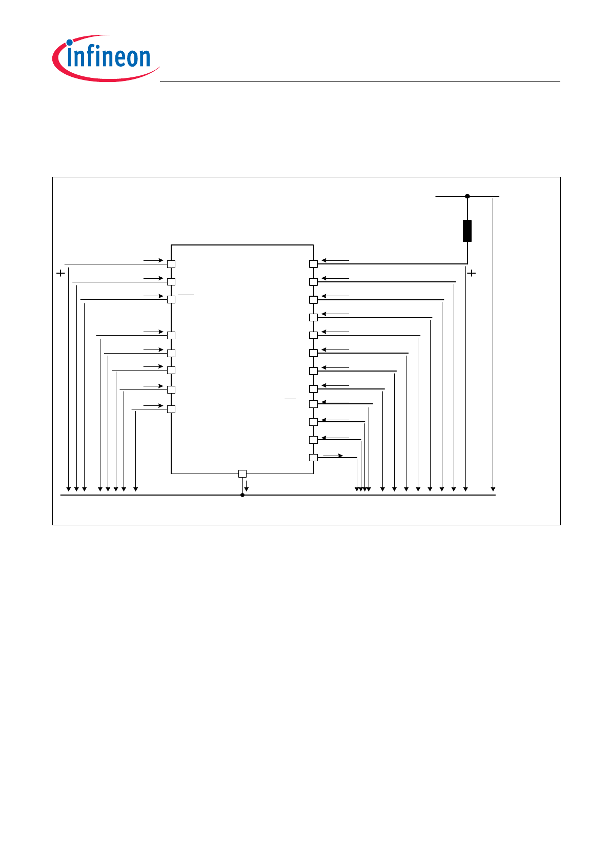
Block Diagram
2
Block Diagram
Figure 1
Block Diagram for the SPIDER - TLE7244SL
Blockdiagram .emf
GND
CS
SI
SCLK
SO
SPI
control,
diagnostic
and
protective
functions
diagnosis
register
VDDA
VDD
RST
OUT3
OUT2
OUT1
OUT7
OUT6
OUT5
OUT4
OUT8
stand-by control
input mux and
control
IN1
IN2
IN3
IN4
LHI
open load
detection
temperature
sensor
gate
control
short circuit
detection
SPI Driver for Enhanced Relay Control
SPIDER - TLE7244SL
Pin Configuration
Datasheet
6
Rev. 1.3, 2011-10-21
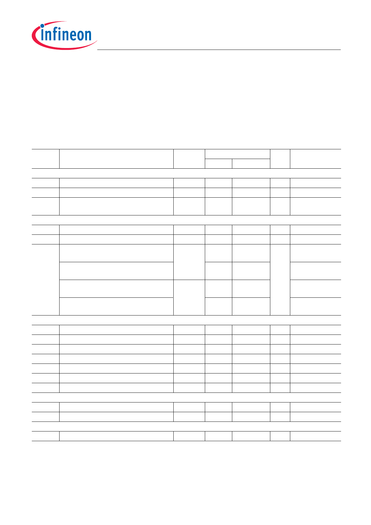
3
Pin Configuration
3.1
Pin Assignment
Figure 2
Pin Configuration
3.2
Pin Definitions and Functions
20
Pin
Symbol
I/O
1)
Function
Power Supply
13
VDD
-
Digital Supply Voltage; Connected to 3.3V or 5V Voltage with Reverse
protection Diode and Filter against EMC
24
VDDA
-
Analog Supply Voltage; Connected to 5V Voltage with Reverse
protection Diode and Filter against EMC
1,2,11,12 GND
-
Ground; common ground for digital, analog and power
Power Stages
3
OUT1
O
Output Channel 1; Drain of power transistor channel 1
4
OUT2
O
Output Channel 2; Drain of power transistor channel 2
5
OUT3
O
Output Channel 3; Drain of power transistor channel 3
6
OUT4
O
Output Channel 4; Drain of power transistor channel 4
7
OUT5
O
Output Channel 5; Drain of power transistor channel 5
8
OUT6
O
Output Channel 6; Drain of power transistor channel 6
9
OUT7
O
Output Channel 7; Drain of power transistor channel 7
10
OUT8
O
Output Channel 8; Drain of power transistor channel 8
Inputs
17
IN1
I
PD Control Input; Digital input 3.3 V or 5V. In case of not used keep open.
16
IN2
I
PD Control Input; Digital input 3.3 V or 5V. In case of not used keep open.
Pinout.emf
(top view )
1
2
3
4
5
6
7
8
9
10
11
12
24
23
22
21
20
19
18
17
16
15
14
13
OUT2
OUT3
OUT4
OUT5
GND
GND
OUT1
GND
GND
OUT6
OUT7
OUT8
IN2
IN3
CS
SCLK
IN1
SI
SO
RST
LHI
IN4
VDDA
VDD
Datasheet
7
Rev. 1.3, 2011-10-21
SPI Driver for Enhanced Relay Control
SPIDER - TLE7244SL
Pin Configuration
15
IN3
I
PD Control Input; Digital input 3.3 V or 5V. In case of not used keep open.
14
IN4
I
PD Control Input; Digital input 3.3 V or 5V. In case of not used keep open.
18
LHI
I
PD Limp Home; Digital input 3.3 V or 5V. In case of not used keep open.
21
RST
I
PD Reset input pin; Digital input 3.3 V or 5V. Low active
SPI
23
CS
I
PU SPI chip select; Digital input 3.3 V or 5V. Low active
20
SCLK
I
PD serial clock; Digital input 3.3 V or 5V.
22
SI
I
PD serial data in; Digital input 3.3 V or 5V.
19
SO
O
serial data out; Digital output with voltage level referring to
V
DD
.
1) O: Output, I: Input,
PD: pull-down resistor integrated,
PU: pull-up resistor integrated
Pin
Symbol
I/O
1)
Function
SPI Driver for Enhanced Relay Control
SPIDER - TLE7244SL
Pin Configuration
Datasheet
8
Rev. 1.3, 2011-10-21
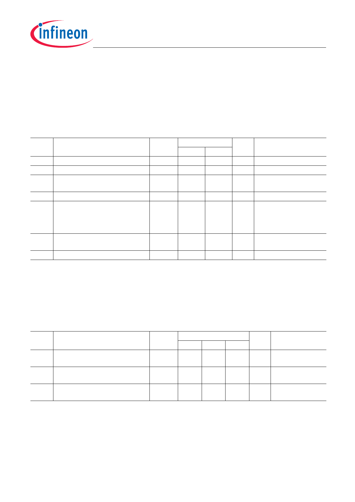
3.3
Voltage and Current naming definition
Figure 3
shows all the terms used in this data sheet, with associated convention for positive values.
Figure 3
Terms
Terms.emf
GND
I
GND
I
D1
OUT1
OUT2
I
D3
OUT3
I
D2
V
DD
I
DD
VDD
V
RST
I
RST
RST
I
DDA
VDDA
V
DDA
OUT4
I
D5
OUT5
OUT6
I
D7
OUT7
I
D4
I
D6
OUT8
I
D8
V
DS1
V
bat
V
DS 6
V
DS8
V
DS7
V
DS2
V
DS4
V
DS3
V
DS 5
I
IN1
IN1
I
IN2
IN2
V
IN1
V
CS
V
SCLK
V
SI
SO
SCLK
SI
CS
V
SO
I
CS
I
SCLK
I
SI
I
SO
I
IN3
IN3
I
IN4
IN4
V
IN 2
V
IN3
V
IN4
I
LHI
LHI
V
LHI
Datasheet
9
Rev. 1.3, 2011-10-21
SPI Driver for Enhanced Relay Control
SPIDER - TLE7244SL
General Product Characteristics
4
General Product Characteristics
4.1
Absolute Maximum Ratings
Absolute Maximum Ratings
1)
Unless otherwise specified:
T
j
= -40
⋅
C to +150
⋅
C;
V
DD
= 3.0 V to V
DDA
,
V
DDA
= 4.5V to 5.5V
all voltages with respect to ground, positive current flowing into pin
1) Not subject to production test, specified by design.
Pos.
Parameter
Symbol
Limit Values
Unit
Conditions
Min.
Max.
Power Supply
4.1.1
Digital supply voltage
V
DD
-0.3
5.5
V
–
4.1.2
Analog supply voltage
V
DDA
-0.3
5.5
V
–
4.1.3
Output voltage for short circuit protection
(single pulse)
V
OUT
0
36
V
–
Power Stages
4.1.4
Load current
I
D
-0.5
0.5
A
–
4.1.5
Voltage at power transistor
V
DS
–
41
V
active clamped
4.1.6
Maximum energy dissipation one
channel
E
AS
mJ
2)
V
bat
=16V,
V
clamp
=45V,
2) Pulse shape represents inductive switch off:
I
D
(t)
=
I
D
(0)
×
(1 -
t
/
t
pulse
); 0 <
t
<
t
pulse
single pulse
–
67
T
j(0)
= 150
°
C
I
D(0)
=0.50 A
repetitive (1 · 10
4
cycles)
E
AR
–
31
T
j(0)
= 105
°
C
I
D(0)
=0.40 A
repetitive (1 · 10
6
cycles)
–
24
T
j(0)
= 105
°
C
I
D(0)
=0.40 A
Logic Pins
4.1.7
IN1,IN2,IN3,IN4;Voltage at input pins
V
IN
-0.3
5.5
V
–
4.1.8
RST; Voltage at reset pin
V
RST
-0.3
5.5
V
–
4.1.9
LHI; Voltage at limp home input pin
V
LHI
-0.3
5.5
V
–
4.1.10
CS; Voltage at chip select
V
CS
-0.3
V
DD
+ 0.3
V
3)
3) level must not exceed
V
DD
+0.3V < 5.5 V
4.1.11
SCLK; Voltage at serial clock pin
V
SCLK
-0.3
V
DD
+ 0.3
V
3)
4.1.12
SI; Voltage at serial input pin
V
SI
-0.3
V
DD
+ 0.3
V
3)
4.1.13
SO; Voltage at serial output pin
V
SO
-0.3
V
DD
+ 0.3
V
3)
Temperatures
4.1.14
Junction Temperature
T
j
-40
150
°
C
–
4.1.15
Storage Temperature
T
stg
-55
150
°
C
–
ESD Susceptibility
4.1.16
ESD Resistivity
V
ESD
-4
4
kV
HBM
4)
4) ESD susceptibility, HBM according to EIA/JESD 22-A114
SPI Driver for Enhanced Relay Control
SPIDER - TLE7244SL
General Product Characteristics
Datasheet
10
Rev. 1.3, 2011-10-21
Note: Stresses above the ones listed here may cause permanent damage to the device. Exposure to absolute
maximum rating conditions for extended periods may affect device reliability.
Note: Integrated protection functions are designed to prevent IC destruction under fault conditions described in the
data sheet. Fault conditions are considered as “outside” normal operating range. Protection functions are
not designed for continuous repetitive operation.
4.2
Functional Range
Note: Within the functional range the IC operates as described in the circuit description. The electrical
characteristics are specified within the conditions given in the related electrical characteristics table.
4.3
Thermal Resistance
Note: This thermal data was generated in accordance with JEDEC JESD51 standards.
For more information, go to
www.jedec.org
.
Pos.
Parameter
Symbol
Limit Values
Unit
Conditions
Min.
Max.
4.2.1
Digital supply voltage
V
DD
3.0
5.5
V
–
4.2.1
Analog supply voltage
V
DDA
4.5
5.5
V
–
4.2.2
extended supply range
V
DDA
4.0
4.5
parameter deviations are
possible
4.2.3
Digital Supply current in reset mode
I
DD(RST)
–
10
µA
T
j
= 85
°
C
4.2.4
Digital supply current
(all channels active)
I
DD(ON)
–
0.5
mA
V
DD
=
V
DDA
= 5 V
V
RST
=
V
CS
=
V
DD
V
SCLK
= 0 V
V
IN
= 0 V
4.2.5
Analog supply current
(all channels active)
I
DDA(ON)
–
5
mA
–
4.2.6
Analog supply turn-ON time
t
DDA(ON)
15
–
µs
V
DDA
= 0V to 5V (linear)
Pos.
Parameter
Symbol
Limit Values
Unit
Conditions
Min.
Typ.
Max.
4.3.7
Junction to Soldering Point
R
thJSP
–
–
25
K/W
1)
2)
1) Not subject to production test, specified by design
2) Specified
R
thJSP
value is simulated at natural convection on a cold plate setup (all pins are fixed to ambient temperature).
T
a
= 25
°
C. LS1 to LS8 are dissipating 1 W power (0.125 W each).
4.3.8
Junction to Ambient
(1s0p+600mm
2
Cu)
R
thJA
–
68
–
K/W
1)
3)
3) Specified
R
thJA
value is according to Jedec JESD51-2,-3 at natural convection on FR4 1s0p board; The product
(Chip+Package) was simulated on a 76.2 x 114.3 x 1.5 mm board with additional heatspreading copper area of 600mm
2
and 70
µ
m thickness.
T
a
= 25
°
C, LS1 to LS8 are dissipating 1 W power (0.125 W each).
4.3.9
Junction to Ambient (2s2p)
R
thJA
–
58
–
K/W
1)
4)
4) Specified
R
thJA
value is according to Jedec JESD51-2,-7 at natural convection on FR4 2s2p board; The product
(Chip+Package) was simulated on a 76.2 x 114.3 x 1.5 mm board with 2 inner copper layers (2 x 70
µ
m Cu, 2 x 35
µ
m Cu).
T
a
= 25
°
C, LS1 to LS8 are dissipating 1 W power (0.125 W each).