

C C M - P F C
I C E 2 P C S 0 6
I C E 2 P C S 0 6 G
S t a n d a l o n e P o w e r F a c t o r
C o r r e c t i o n ( P F C ) C o n t r o l l e r i n
C o n t i n u o u s C o n d u c t i o n M o d e
( C C M ) w i t h I n p u t B r o w n - O u t
P r o t e c t i o n
N e v e r
s t o p
t h i n k i n g .
V e r s i o n 1 . 1 , M a r 2 0 1 0
Power Management & Supply

Edition 2010-03-22
Published by
Infineon Technologies AG
81726 München, Germany
©
2007 Infineon Technologies AG
All Rights Reserved.
Legal Disclaimer
The information given in this document shall in no event be regarded as a guarantee of conditions or
characteristics. With respect to any examples or hints given herein, any typical values stated herein and/or any
information regarding the application of the device, Infineon Technologies hereby disclaims any and all warranties
and liabilities of any kind, including without limitation, warranties of non-infringement of intellectual property rights
of any third party.
Information
For further information on technology, delivery terms and conditions and prices please contact your nearest
Infineon Technologies Office (
www.infineon.com
).
Warnings
Due to technical requirements components may contain dangerous substances. For information on the types in
question please contact your nearest Infineon Technologies Office.
Infineon Technologies Components may be used in life-support devices or systems only with the express written
approval of Infineon Technologies, if a failure of such components can reasonably be expected to cause the failure
of that life-support device or system, or to affect the safety or effectiveness of that device or system. Life support
devices or systems are intended to be implanted in the human body, or to support and/or maintain and sustain
and/or protect human life. If they fail, it is reasonable to assume that the health of the user or other persons may
be endangered.
For questions on technology, delivery and prices please contact the Infineon Technologies Offices in Germany or
the Infineon Technologies Companies and Representatives worldwide: see our webpage at http://
www.infineon.com
CCM-PFC
Revision History:
Datasheet
Previous Version: V1.0
Page
Subjects(major changes since last version)
18&19
Package outline change
CCM-PFC
ICE2PCS06
ICE2PCS06G
Version 1.1
3
Mar 2010
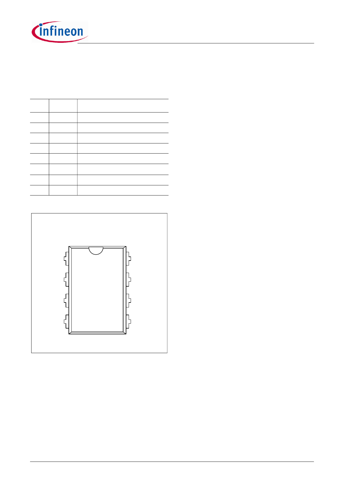
Type
Package
ICE2PCS06
PG-DIP-8
ICE2PCS06G
PG-DSO-8
Standalone Power Factor Correction (PFC)
Controller in Continuous Conduction Mode
(CCM) with Input Brown-Out Protection
ICE2PCS06
PG-DIP-8
ICE2PCS06G
PG-DSO-8
Product Highlights
•
Leadfree DIP and DSO Package
•
Wide Input Range
•
Direct sensing, Input Brown-Out Detection
•
Optimized for applications which require fast Startup
•
Output Power Controllable by External Sense Resistor
•
Fast Output Dynamic Response during Load Jumps
•
Trimmed, internal fixed Switching Frequency (65kHz)
Features
•
Ease of Use with Few External Components
•
Supports Wide Input Range
•
Average Current Control
•
External Current and Voltage Loop Compensation
for Greater User Flexibility
•
Trimmed internal fixed Switching Frequency
(65kHz+5% at 25
o
C)
•
Direct sensing, Input Brown-Out Detection
with Hysteresis
•
Short Startup(SoftStart) duration
•
Max Duty Cycle of 95% (at 25
o
C)
•
Trimmed Internal Reference Voltage (3V+2% at
25
o
C)
•
VCC Under-Voltage Lockout
•
Cycle by Cycle Peak Current Limiting
•
Output Over-Voltage Protection
•
Open Loop Detection
•
Soft Overcurrent Protection
•
Enhanced Dynamic Response
•
Fulfills Class D Requirements of IEC 1000-3-2
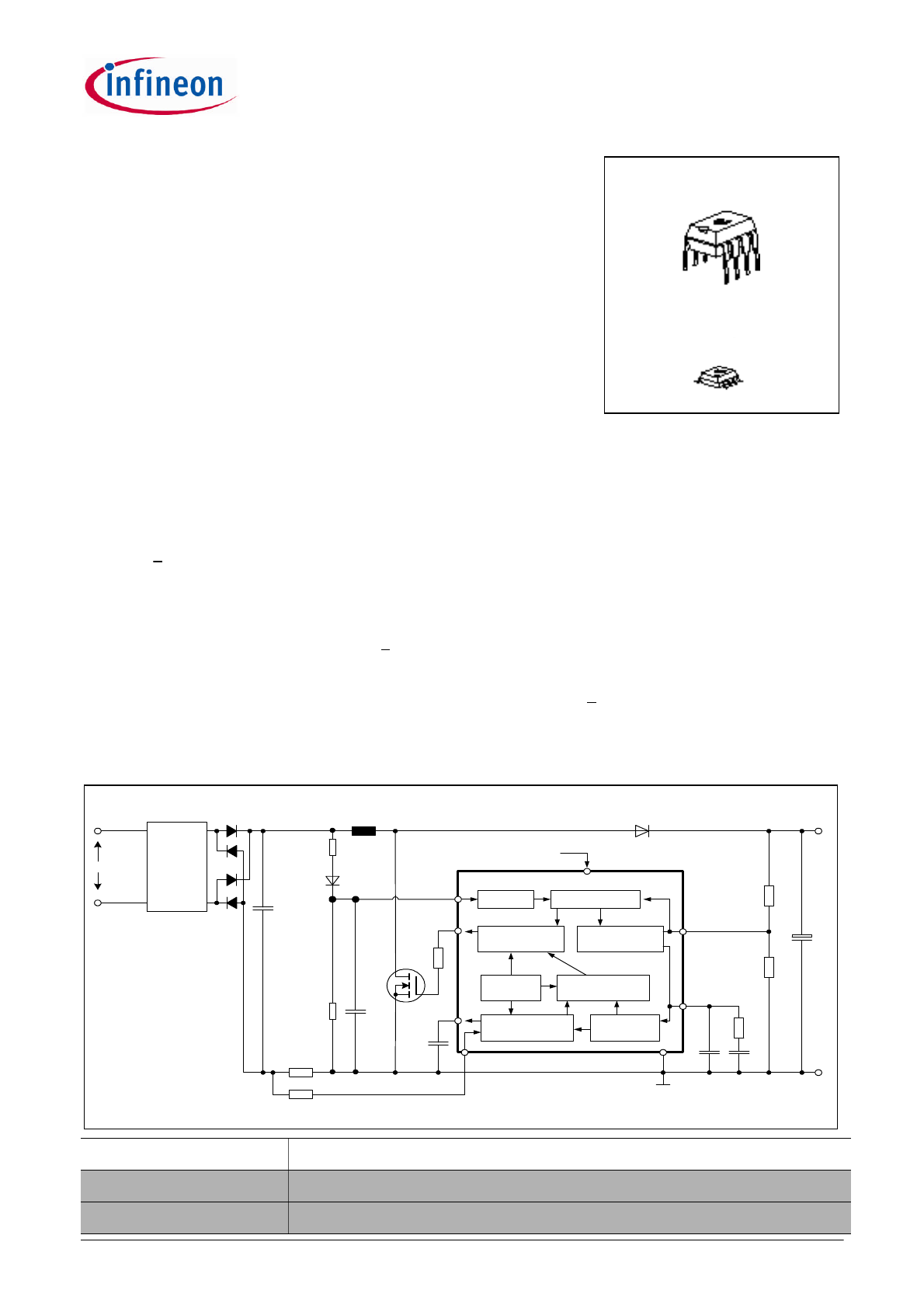
Description
The ICE2PCS06/G is a 8-pin wide input range controller
IC for active power factor correction converters. It is de-
signed for converters in boost topology, and requires few
external components. Its power supply is recommended
to be provided by an external auxiliary supply which will
switch on and off the IC.
The IC operates in the CCM with average current control,
and in DCM only under light load condition. The switching
frequency is trimmed and fixed internally at 65kHz. Both
current and voltage loop compensations are done exter-
nally to allow full user control.
There are various protection features incorporated to en-
sure safe system operation conditions. The internal refer-
ence is trimmed (3V+2%) to ensure precise protection and
output control level.
85 ... 265 V A C
E M I-Filter
V oltage Loop
C om pensation
P rotection U nit
Fixed
O scillator
C urrent Loop
C om pensation
P W M Logic
D river
IC E 2P C S 02 /G
C C M P FC
V C C
A uxiliary S upply
V
O U T
Typ ical A p plication
R am p
G enerator
IC O M P
V S E N S E
V C O M P
IS E N S E
G N D
N onlinear
G ain
G A TE
V IN S
B row n-out
d

CCM-PFC
ICE2PCS06/G
Version 1.1
4
Mar 2010
1
Pin Configuration and Functionality . . . . . . . . . . . . . . . . . . . . . . . . . . . . . 5
1.1
Pin Configuration . . . . . . . . . . . . . . . . . . . . . . . . . . . . . . . . . . . . . . . . . . . . . . 5
1.2
Pin Functionality . . . . . . . . . . . . . . . . . . . . . . . . . . . . . . . . . . . . . . . . . . . . . . 5
2
Representative Block diagram . . . . . . . . . . . . . . . . . . . . . . . . . . . . . . . . . . 6
3
Functional Description . . . . . . . . . . . . . . . . . . . . . . . . . . . . . . . . . . . . . . . . 7
3.1
General . . . . . . . . . . . . . . . . . . . . . . . . . . . . . . . . . . . . . . . . . . . . . . . . . . . . . 7
3.2
Power Supply . . . . . . . . . . . . . . . . . . . . . . . . . . . . . . . . . . . . . . . . . . . . . . . . 7
3.3
Start-up . . . . . . . . . . . . . . . . . . . . . . . . . . . . . . . . . . . . . . . . . . . . . . . . . . . . . 7
3.4
System Protection . . . . . . . . . . . . . . . . . . . . . . . . . . . . . . . . . . . . . . . . . . . . . 8
3.4.1
Input Brown-Out Protection (IBOP) . . . . . . . . . . . . . . . . . . . . . . . . . . . . . . 8
3.4.2
Soft Over Current Control (SOC) . . . . . . . . . . . . . . . . . . . . . . . . . . . . . . . 9
3.4.3
Peak Current Limit (PCL) . . . . . . . . . . . . . . . . . . . . . . . . . . . . . . . . . . . . . 9
3.4.4
Open Loop Protection (OLP) . . . . . . . . . . . . . . . . . . . . . . . . . . . . . . . . . . . 9
3.4.5
Over-Voltage Protection (OVP) . . . . . . . . . . . . . . . . . . . . . . . . . . . . . . . . . 9
3.5
Fixed Switching Frequency . . . . . . . . . . . . . . . . . . . . . . . . . . . . . . . . . . . . . . 9
3.6
Average Current Control . . . . . . . . . . . . . . . . . . . . . . . . . . . . . . . . . . . . . . . 10
3.6.1
Complete Current Loop . . . . . . . . . . . . . . . . . . . . . . . . . . . . . . . . . . . . . . 10
3.6.2
Current Loop Compensation . . . . . . . . . . . . . . . . . . . . . . . . . . . . . . . . . . 10
3.6.3
Pulse Width Modulation (PWM) . . . . . . . . . . . . . . . . . . . . . . . . . . . . . . . 10
3.6.4
Nonlinear Gain Block . . . . . . . . . . . . . . . . . . . . . . . . . . . . . . . . . . . . . . . 10
3.7
PWM Logic . . . . . . . . . . . . . . . . . . . . . . . . . . . . . . . . . . . . . . . . . . . . . . . . . 11
3.8
Voltage Loop . . . . . . . . . . . . . . . . . . . . . . . . . . . . . . . . . . . . . . . . . . . . . . . . 11
3.8.1
Voltage Loop Compensation . . . . . . . . . . . . . . . . . . . . . . . . . . . . . . . . . . 11
3.8.2
Enhanced Dynamic Response . . . . . . . . . . . . . . . . . . . . . . . . . . . . . . . . 11
3.9
Output Gate Driver . . . . . . . . . . . . . . . . . . . . . . . . . . . . . . . . . . . . . . . . . . . 11
4
Electrical Characteristics . . . . . . . . . . . . . . . . . . . . . . . . . . . . . . . . . . . . . 13
4.1
Absolute Maximum Ratings . . . . . . . . . . . . . . . . . . . . . . . . . . . . . . . . . . . . 13
4.2
Operating Range . . . . . . . . . . . . . . . . . . . . . . . . . . . . . . . . . . . . . . . . . . . . . 13
4.3
Characteristics . . . . . . . . . . . . . . . . . . . . . . . . . . . . . . . . . . . . . . . . . . . . . . 14
4.3.1
Supply Section . . . . . . . . . . . . . . . . . . . . . . . . . . . . . . . . . . . . . . . . . . . . 14
4.3.2
PWM Section . . . . . . . . . . . . . . . . . . . . . . . . . . . . . . . . . . . . . . . . . . . . . 14
4.3.3
System Protection Section . . . . . . . . . . . . . . . . . . . . . . . . . . . . . . . . . . . 15
4.3.4
Current Loop Section . . . . . . . . . . . . . . . . . . . . . . . . . . . . . . . . . . . . . . . 15
4.3.5
Voltage Loop Section . . . . . . . . . . . . . . . . . . . . . . . . . . . . . . . . . . . . . . . 16
4.3.6
Driver Section . . . . . . . . . . . . . . . . . . . . . . . . . . . . . . . . . . . . . . . . . . . . . 17
5
Outline Dimension . . . . . . . . . . . . . . . . . . . . . . . . . . . . . . . . . . . . . . . . . . 18
Version 1.1
5
Mar 2010
CCM-PFC
ICE2PCS06/G
Pin Configuration and Functionality
1
Pin Configuration and Functionality
1.1
Pin Configuration
Figure 1
Pin Configuration (top view)
1.2
Pin Functionality
GND (Ground)
The ground potential of the IC.
ICOMP (Current Loop Compensation)
Low pass filter and compensation of the current control
loop. The capacitor which is connected at this pin
integrates the output current of OTA2 and averages the
current sense signal.
ISENSE (Current Sense Input)
The ISENSE Pin senses the voltage drop at the
external sense resistor (R1). This is the input signal for
the average current regulation in the current loop. It is
also fed to the peak current limitation block.
During power up time, high inrush currents cause high
negative voltage drop at R1, driving currents out of pin
3 which could be beyond the absolute maximum
ratings. Therefore a series resistor (R2) of around
220
W is recommended in order to limit this current into
the IC.
VINS (Brown-out Sense Input)
This VINS pin senses a filtered input voltage divider
and detects for the input voltage Brown-out condition.
A Brown-out condition of VINS<0.71V, shuts down the
IC. The IC turns on at VINS>1.5V.
VSENSE (Voltage Sense/Feedback)
The output bus voltage is sensed at this pin via a
resistive divider. The reference voltage for this pin is
3V.
VCOMP (Voltage Loop Compensation)
This pin provides the compensation of the output
voltage loop with a compensation network to ground
(see Figure 2).
VCC (Power Supply)
The VCC pin is the positive supply of the IC and should
be connected to an external auxiliary supply. The
operating range is between 11V and 26V. The turn-on
threshold is at 11.8V and under voltage occurs at 11V.
There is no internal clamp for a limitation of the power
supply.
GATE
The GATE pin is the output of the internal driver stage.
Its gate drive voltage is internally clamped at 15.0V
(typically).
Pin
Symbol
Function
1
GND
IC Ground
2
ICOMP
Current Loop Compensation
3
ISENSE
Current Sense Input
4
VINS
Brown-out Sense Input
5
VCOMP
Voltage Loop Compensation
6
VSENSE V
OUT
Sense (Feedback) Input
7
VCC
IC Supply Voltage
8
GATE
Gate Drive Output
Package PG-DIP-8 / PG-DSO-8
1
6
7
8
4
3
2
5
GATE
GND
ICOMP
ISENSE
VCC
VSENSE
VINS
VCOMP
CCM-PFC
ICE2PCS06/G
Representative Block diagram
Version 1.1
6
Mar 2010
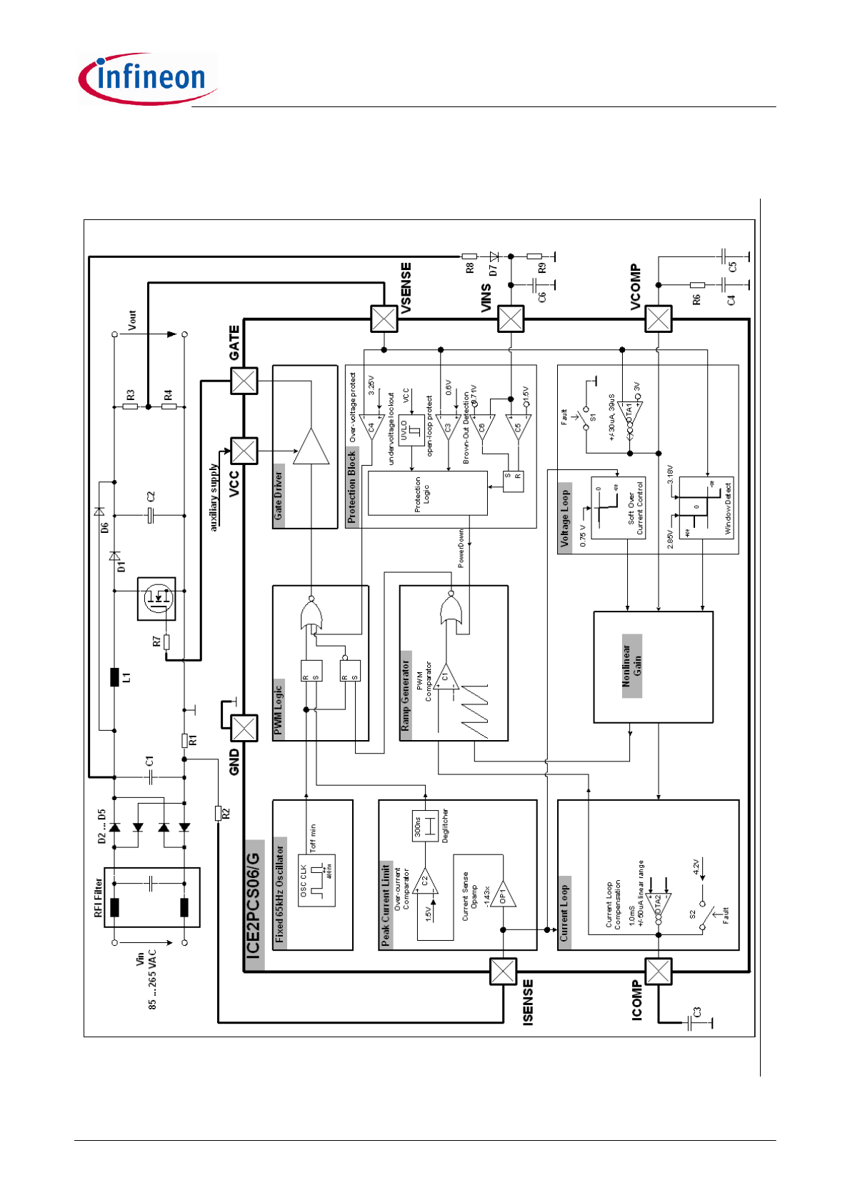
2
Representative Block diagram
Figure 2
Representative Block diagram
CCM-PFC
ICE2PCS06/G
Functional Description
Version 1.1
7
Mar 2010
3.1
General
The ICE2PCS06/G is a 8 pin control IC for power factor
correction converters. It comes in both DIP and DSO
packages and is suitable for wide range line input
applications from 85 to 265 VAC. The IC supports
converters in boost topology and it operates in
continuous conduction mode (CCM) with average
current control.
It is a design derivative from the ICE2PCS01/G with the
differences in the supporting functions, namely the
input brown-out detection and internal fixed switching
frequency 65kHz.
The IC operates with a cascaded control; the inner
current loop and the outer voltage loop. The inner
current loop of the IC controls the sinusoidal profile for
the average input current. It uses the dependency of
the PWM duty cycle on the line input voltage to
determine the corresponding input current. This means
the average input current follows the input voltage as
long as the device operates in CCM. Under light load
condition, depending on the choke inductance, the
system may enter into discontinuous conduction mode
(DCM) resulting in a higher harmonics but still meeting
the Class D requirement of IEC 1000-3-2.
The outer voltage loop controls the output bus voltage.
Depending on the load condition, OTA1 establishes an
appropriate voltage at VCOMP pin which controls the
amplitude of the average input current.
The IC is equipped with various protection features to
ensure safe operating condition for both the system
and device.
3.2
Power Supply
An internal under voltage lockout (UVLO) block
monitors the VCC power supply. As soon as it exceeds
11.8V and both voltages at pin 6 (VSENSE) >0.6V and
pin 4 (VINS) >1.5V, the IC begins operating its gate
drive and performs its Startup as shown in Figure 3.
.
Figure 3
State of Operation respect to VCC
If VCC drops below 11V, the IC is off. The IC will then
be consuming typically 300
mA, whereas consuming
10mA during normal operation.
The IC can be turned off and forced into standby mode
by pulling down the voltage at pin 6 (VSENSE) to lower
than
0.6V.
In
this
standby
mode,
the
current
consumption is reduced to 300
mA. Other condition that
can result in the standby mode is when a Brown-out
condition occurs, ie pin 4 (VINS) <0.71V.
3.3
Start-up
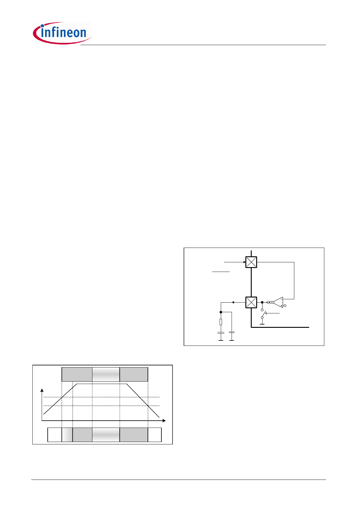
Figure 4 shows the operation of voltage loop’s OTA1
during startup. The VCOMP pin is pull internally to
ground via switch S1 during UVLO and other fault
conditions (see later section on “System Protection”).
During power up when V
OUT
is less than 83% of the
rated level, OTA1 sources an output current, maximum
30
mA into the compensation network at pin 5 (VCOMP)
causing the voltage at this pin to rise linearly. This
results in a controlled linear increase of the input
current from 0A thus reducing the stress on the
external component.
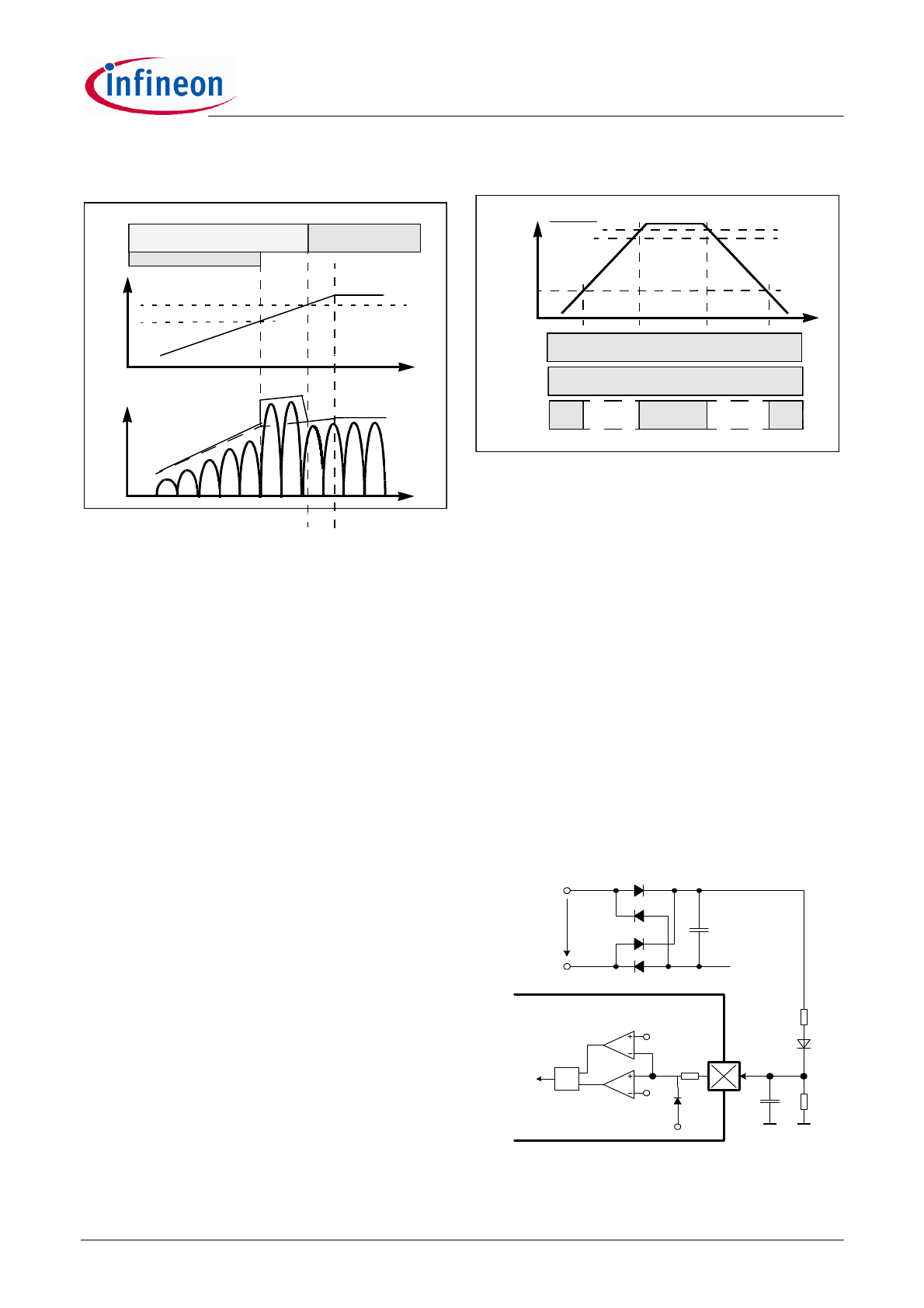
Figure 4
Startup Circuit
As V
OUT
has not reached within 5% from the rated
value, VCOMP voltage is level-shifted by the window
detect block as shown in Figure 5, to ensure there is
fast boost up output voltage.
When V
OUT
approaches its rated value, OTA1’s
sourcing current drops and so does the level shift of the
window detect block is removed. The normal voltage
loop then takes control.
V
CC
(V
VSENSE
> 0.6 V)
AND (V
VINS
> 1.5 V)
11.8 V
11.0 V
t
OFF
Start
Up
Open loop/
Standby
Normal
Operation
IC's
State
OFF
Normal
Operation
(V
VSENSE
< 0.6 V)
OR (V
VINS
< 0.8 V)
(V
VSENSE
> 0.6 V)
AND (V
VINS
> 1.5 V)
VCOMP
C5
C4
VSENSE
OTA1
3V
ICE2PCS06/G
protect
R3 + R4
R4
x V
OUT
)
(
R6
S1
3
Functional Description
CCM-PFC
ICE2PCS06/G
Functional Description
Version 1.1
8
Mar 2010
.
Figure 5
Startup with controlled maximum current
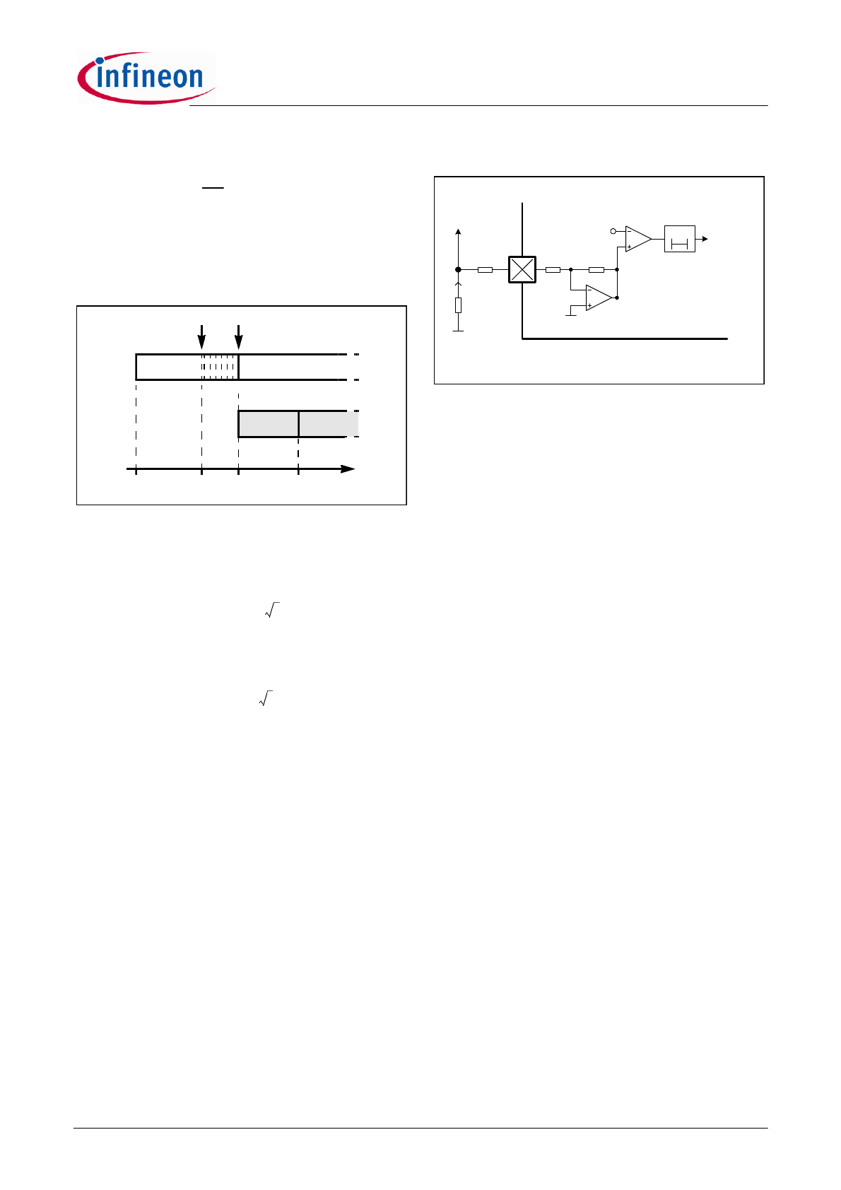
3.4
System Protection
The IC provides several protection features in order to
ensure the PFC system in safe operating range:
•
VCC Undervoltage Lockout (UVLO)
•
Input Brown-out Detection (IBOP)
•
Soft Over Current Control (SOC)
•
Peak Current Limit (PCL)
•
Open-Loop Detection (OLP)
•
Output Over-Voltage Protection (OVP)
After the system is supplied with the correct level of
VCC and V
IN
, the system will enter into its normal mode
of operation. Figure 6 shows situation when these
protections features are active, as a function of the
output voltage V
OUT
.
An activation of the UVLO, IBOP and OLP results in the
internal fault signal going high and brings the IC into the
standby mode.
As the function of UVLO has already described in the
earlier “Power Supply” section, the following sections
continue
to
describe
the
functionality
of
these
protection features.
Figure 6
Protection Features
3.4.1
Input Brown-Out Protection (IBOP)
Brown-out occurs when the input voltage V
IN
falls below
the minimum input voltage of the design (i.e. 85V for
universal input voltage range) and the VCC has not
entered into the V
CCUVLO
level yet. For a system without
IBOP, the boost converter will increasingly draw a
higher current from the mains at a given output power
which may exceed the maximum design values of the
input current.
ICE2PCS06/G provides a new IBOP feature whereby it
senses directly the input voltage for Input Brown-Out
condition
via
an
external
resistor/capacitor/diode
network as shown in Figure 7. This network provides a
filtered value of V
IN
which turns the IC on when the
voltage at pin 4 (VINS) is more than 1.5V. The IC enters
into the standby mode when VINS goes below 0.71V.
The hysteresis prevents the system to oscillate
between normal and standby mode. Note also that V
IN
needs to at least 20% of the rated V
OUT
in order to
overcome OLP and powerup the system.
Figure 7
Input Brown-Out Protection (IBOP)
av(I
IN
)
V
OUT
t
V
OUT
=rated
95%rated
Window Detect
Normal Control
t
Max Vcomp current
83%rated
VCOMP
Level-shifted VCOMP
t
V
OUT
PCL / SOC
20%
100%
OLP
OLP
108%
OVP
V
OUT,Rated
UVLO / IBOP
Supply
related
Current
related
Output
related
ICE2PCS06/G
85 ... 265 VAC
Vin
C1
D2 ... D5
VINS
C4
C5
R
S
1.5V
0.71V
Brow n-Out Detection
R8
R9
C6
D7
brown-out
80k
3.5V
CCM-PFC
ICE2PCS06/G
Functional Description
Version 1.1
9
Mar 2010
3.4.2
Soft Over Current Control (SOC)
The IC is designed not to support any output power
that corresponds to a voltage lower than -0.75V at the
ISENSE pin. A further increase in the inductor current,
which results in a lower ISENSE voltage, will activate
the Soft Over Current Control (SOC). This is a soft
control as it does not directly switch off the gate drive.
It acts on the nonlinear gain block to result in a reduced
PWM duty cycle.
Figure 8
SOC and PCL Protection as function of
V
ISENSE
The rated output power with a minimum V
IN
(V
INMIN
) is
Due to the internal parameter tolerance, the maximum
power with V
INMIN
is
3.4.3
Peak Current Limit (PCL)
The IC provides a cycle by cycle peak current limitation
(PCL). It is active when the voltage at pin 3 (ISENSE)
reaches -1.04V. This voltage is amplified by OP1 by a
factor of -1.43 and connected to comparator C2 with a
reference voltage of 1.5V as shown in Figure 9. A
deglitcher with 300ns after the comparator improves
noise immunity to the activation of this protection.
Figure 9
Peak Current Limit (PCL)
3.4.4
Open Loop Protection (OLP)
Whenever VSENSE voltage falls below 0.6V, or
equivalently V
OUT
falls below 20% of its rated value, it
indicates an open loop condition (i.e. VSENSE pin not
connected) or an insufficient input voltage V
IN
for
normal operation. In this case, most of the blocks within
the IC will be shutdown. It is implemented using
comparator C3 with a threshold of 0.6V as shown in the
IC block diagram in Figure 2.
3.4.5
Over-Voltage Protection (OVP)
Whenever V
OUT
exceeds the rated value by 5%, the
over-voltage protection OVP is active as shown in
Figure 6. This is implemented by sensing the voltage at
pin VSENSE with respect to a reference voltage of
3.15V. A VSENSE voltage higher than 3.15V will
immediately reduce the output duty cycle, bypassing
the normal voltage loop control. This results in a lower
input power to reduce the output voltage V
OUT
. A
VSENSE voltage higher than 3.25V will immediately
turn off the gate, thereby preventing damage to bus
capacitor.
3.5
Fixed Switching Frequency
ICE2PCS06/G
has
an
internally
fixed
switching
frequency as opposed to the ICE2PCS01/G which can
be externally set. This frequency is trimmed to 65kHz
with an accuracy ±5% at 25
o
C.
V
ISENSE
-0.61V -0.75V
-1.04V
Normal
Operation
SOC
PCL
P
OUT
(rated)
IC’s
State
0
P
OUT
(max)
P
OUT
rated
(
)
V
IN MIN
0.61
R1
2
×
-------------------
´
=
P
OUT
ma x
(
)
V
INMIN
0.75
R1
2
×
-------------------
´
=
ISENSE
ICE2PCS06/G
R1
R2
I
INDUCTOR
OP1
1.43x
Current Limit
300ns
C2
Deglitcher
Turn Off
Driver
1.5V
Full-wave
Rectifier
CCM-PFC
ICE2PCS06/G
Functional Description
Version 1.1
10
Mar 2010
3.6
Average Current Control
3.6.1
Complete Current Loop
The complete system current loop is shown in Figure
10.
Figure 10
Complete System Current Loop
It consists of the current loop block which averages the
voltage at pin ISENSE, resulted from the inductor
current flowing across R1. The averaged waveform is
compared with an internal ramp in the ramp generator
and PWM block. Once the ramp crosses the average
waveform, the comparator C1 turns on the driver stage
through the PWM logic block. The Nonlinear Gain block
defines the amplitude of the inductor current. The
following sections describe the functionality of each
individual blocks.
3.6.2
Current Loop Compensation
The compensation of the current loop is done at the
ICOMP pin. This is the OTA2 output and a capacitor C3
has to be installed at this node to ground (see Figure
10). Under normal mode of operation, this pin gives a
voltage which is proportional to the averaged inductor
current. This pin is internally shorted to 4.2V in the
event of standby mode.
3.6.3
Pulse Width Modulation (PWM)
The IC employs an average current control scheme in
continuous conduction mode (CCM) to achieve the
power factor correction.
Assuming the voltage loop is working and output
voltage is kept constant, the off duty cycle D
OFF
for a
CCM PFC system is given as
From the above equation, D
OFF
is proportional to V
IN
.
The objective of the current loop is to regulate the
average inductor current such that it is proportional to
the off duty cycle D
OFF
, and thus to the input voltage
V
IN
. Figure 11 shows the scheme to achieve the
objective.
Figure 11
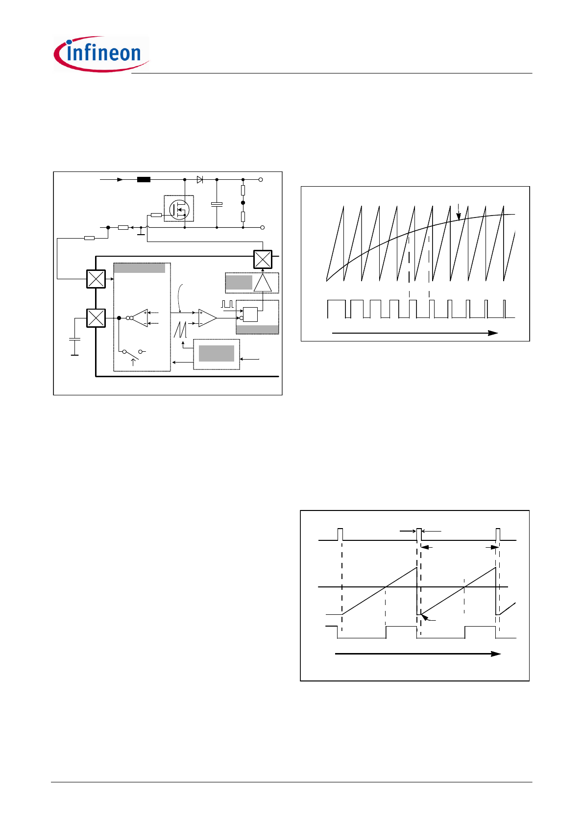
Average Current Control in CCM
The PWM is performed by the intersection of a ramp
signal with the averaged inductor current at pin 5
(ICOMP). The PWM cycle starts with the Gate turn off
for a duration of T
OFFMIN
(400ns typ.) and the ramp is
kept discharged. The ramp is then allowed to rise after
T
OFFMIN
expires. The off time of the boost transistor
ends at the intersection of the ramp signal and the
averaged current waveform. This results in the
proportional relationship between the average current
and the off duty cycle D
OFF
.
Figure 12 shows the timing diagrams of T
OFFMIN
and the
PWM waveforms.
Figure 12
Ramp and PWM waveforms
3.6.4
Nonlinear Gain Block
The nonlinear gain block controls the amplitude of the
regulated inductor current. The input of this block is the
R
S
ICE2PCS06/G
Vout
L1
C2
R3
R4
Gate
Driver
D1
From
Full-wave
Retifier
GATE
R1
R2
OTA2
ICOMP
4.2V
Current Loop
Compensation
Current Loop
Nonlinear
Gain
1.0mS
+/-50uA (linear range)
C3
S2
Fault
ISENSE
C1
PWM
Comparator
PWM Logic
Q
Input From
Voltage Loop
voltage
proportional to
averaged
Inductor current
R7
D
O FF
V
I N
V
OUT
--------------
=
t
ave(I
IN
) at ICOMP
ramp profile
GATE
drive
T
OFFMIN
400ns
V
CREF
(1)
V
RAMP
PWM
ramp
released
PWM cycle
(1)
V
CREF
is a function of V
ICOMP
t