
Data Sheet
1
Features
•
Micro power design
•
2.4 V to 5.5 V battery operation
•
High sensitivity and high stability of the
magnetic switching points
•
High resistance to mechanical stress
•
Digital output signal
•
Switching for both poles of a magnet (omnipolar)
•
Programming pin for the switching
direction of the output
•
Not suitable for automotive application
Functional Description
The TLE 4917 is an Integrated Hall-Effect Sensor designed specifically to meet the
requirements of low-power devices. e.g. as an On/Off switch in Cellular Flip-Phones, with
battery operating voltages of 2.4V – 5.5V.
Precise magnetic switching points and high temperature stability are achieved through the
unique design of the internal circuit.
An onboard clock scheme is used to reduce the average operating current of the IC.
During the operate phase the IC compares the actual magnetic field detected with the
internally compensated switching points. The output Q is switched at the end of each
operating phase.
During the Stand-by phase the output stage is latched and the current consumption of the
device reduced to some µA.
The IC switching behaviour is omnipolar, i.e. it can be switched on with either the North or
South pole of a magnet.
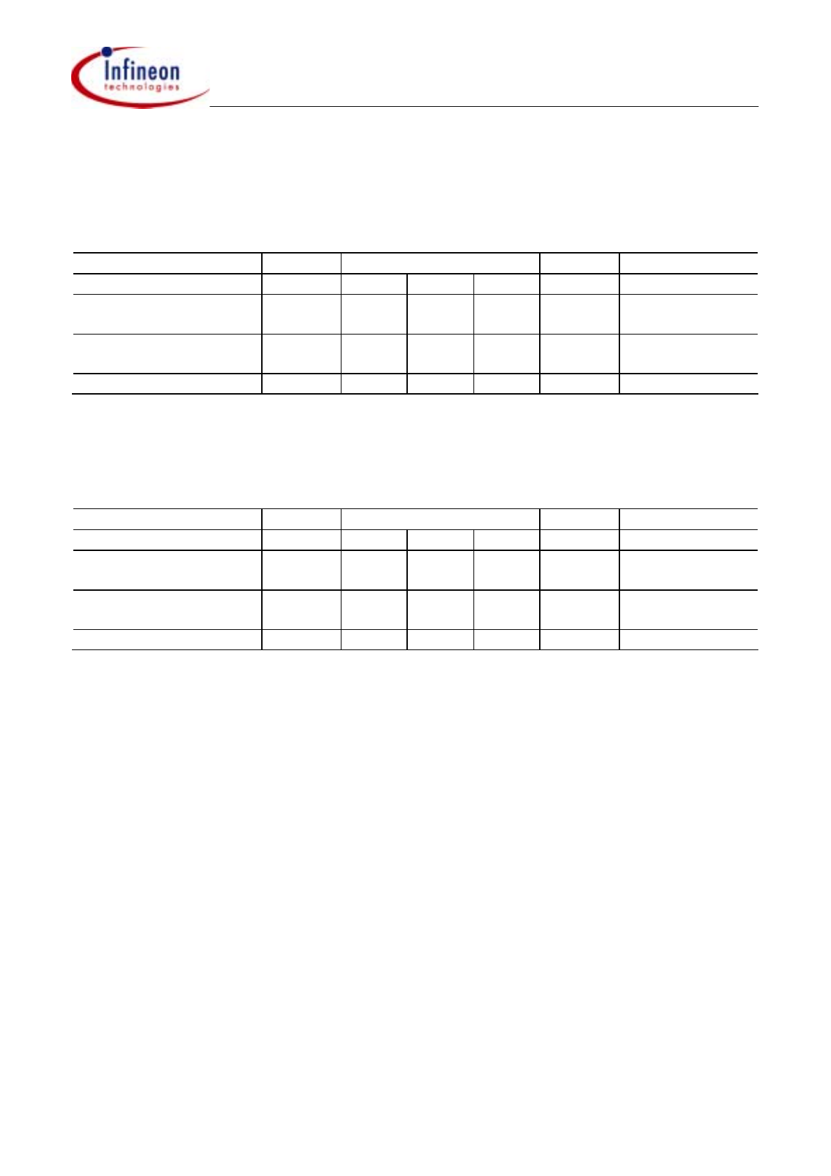
The PRG pin can be connected to V
S
which holds the output V
Q
at a High level for B=0mT;
conversely the output V
Q
can be inverted by connecting the PRG pin to GND, which will
hold the output V
Q
at a Low level for B=0mT. In this later case the presence of an adequate
magnetic field will cause the output V
Q
to switch to a High level ( i.e. off state ).
Type Marking
Ordering
Code
Package
TLE 4917
17s
Q62705K 605
P-TSOP6-6-2
Low Power Hall Switch
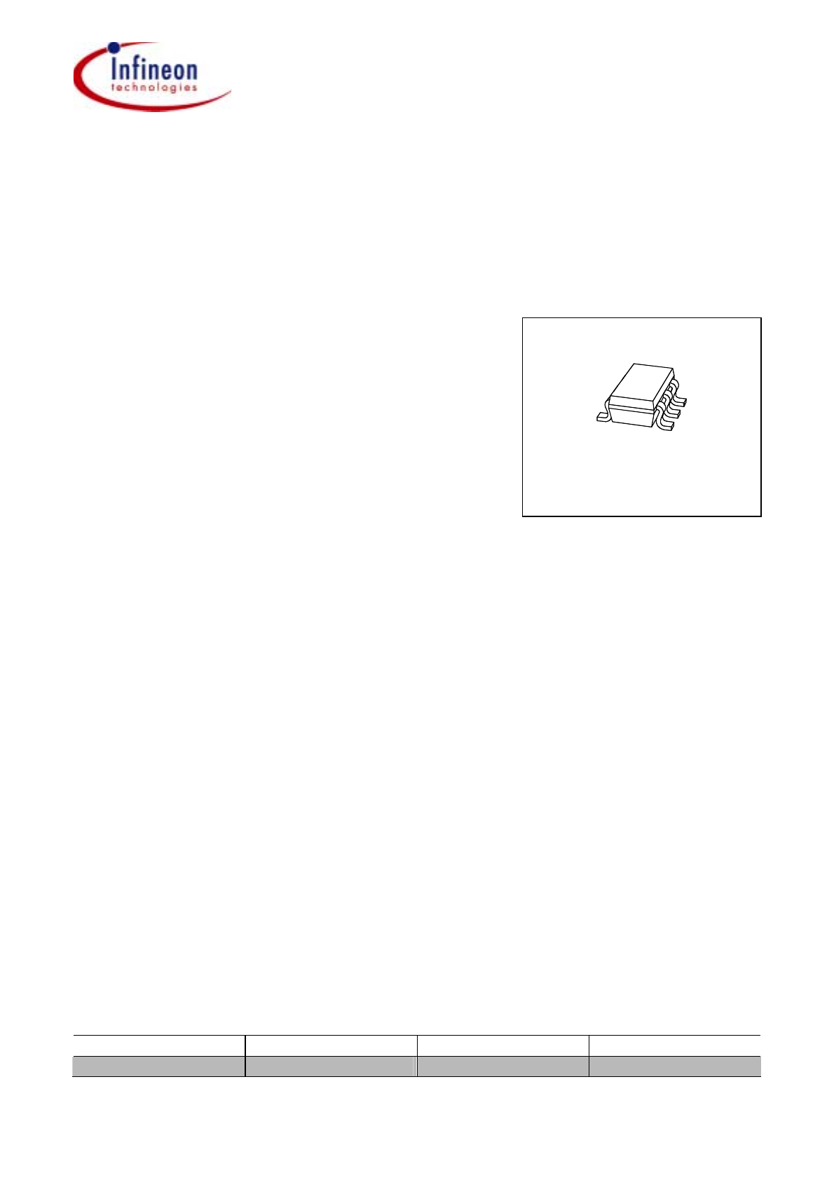
TLE 4917
P-TSOP6-6-2
Data Sheet
2
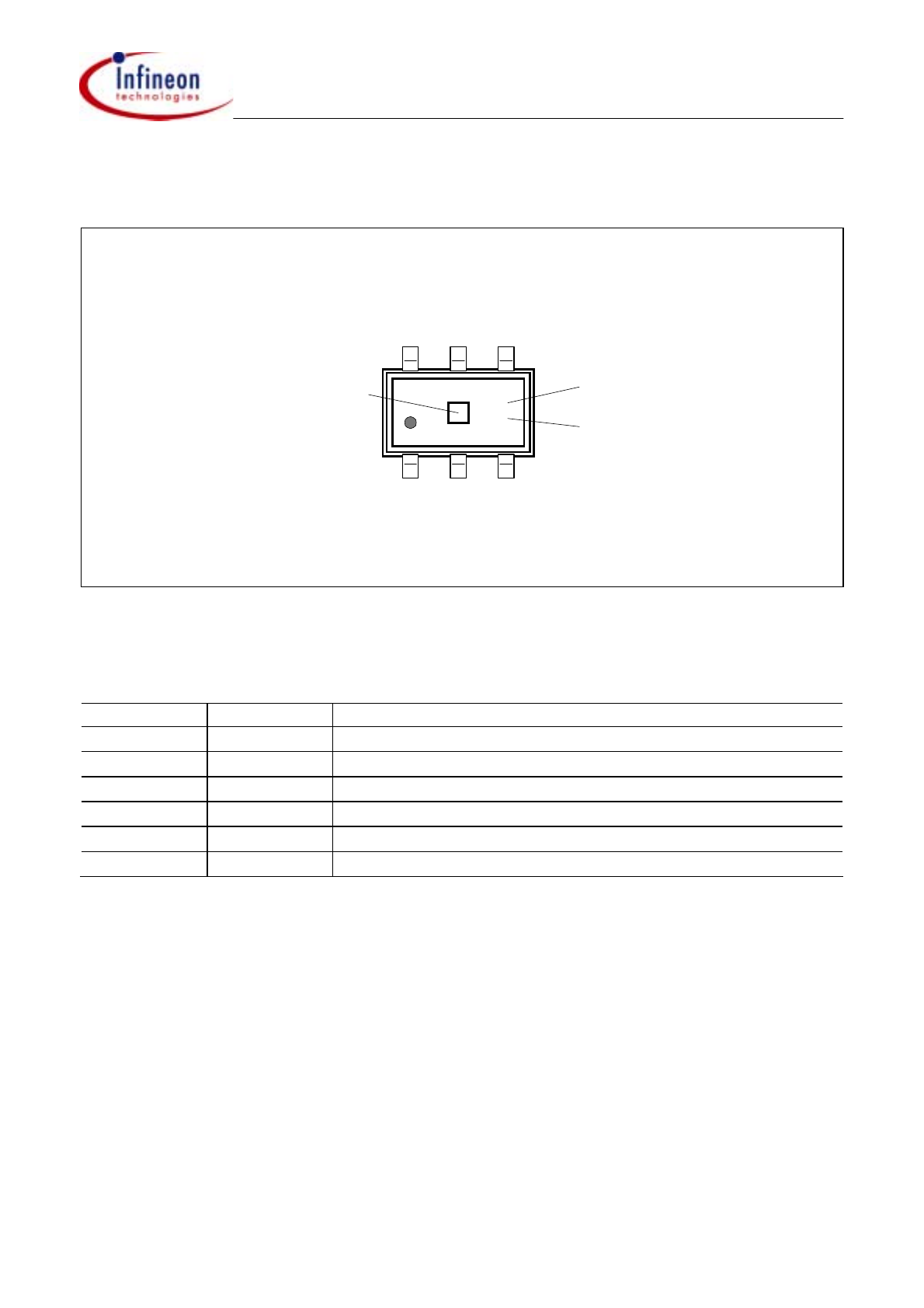
Pin Configuration
(top view)
AEP02801_C
PRG
6
5
GND
4
GND
V
S
GND
Q
1
2
3
Top View
Sensitive Area
17
S
ym
month
year
Figure 1
Pin Definitions and Functions
Pin
Symbol Function
1
V
S
Supply Voltage
2
GND
Ground
3
Q
Open Drain Input
4
GND
Ground
5
GND
Ground
6
PRG
Programming Input
Data Sheet
3
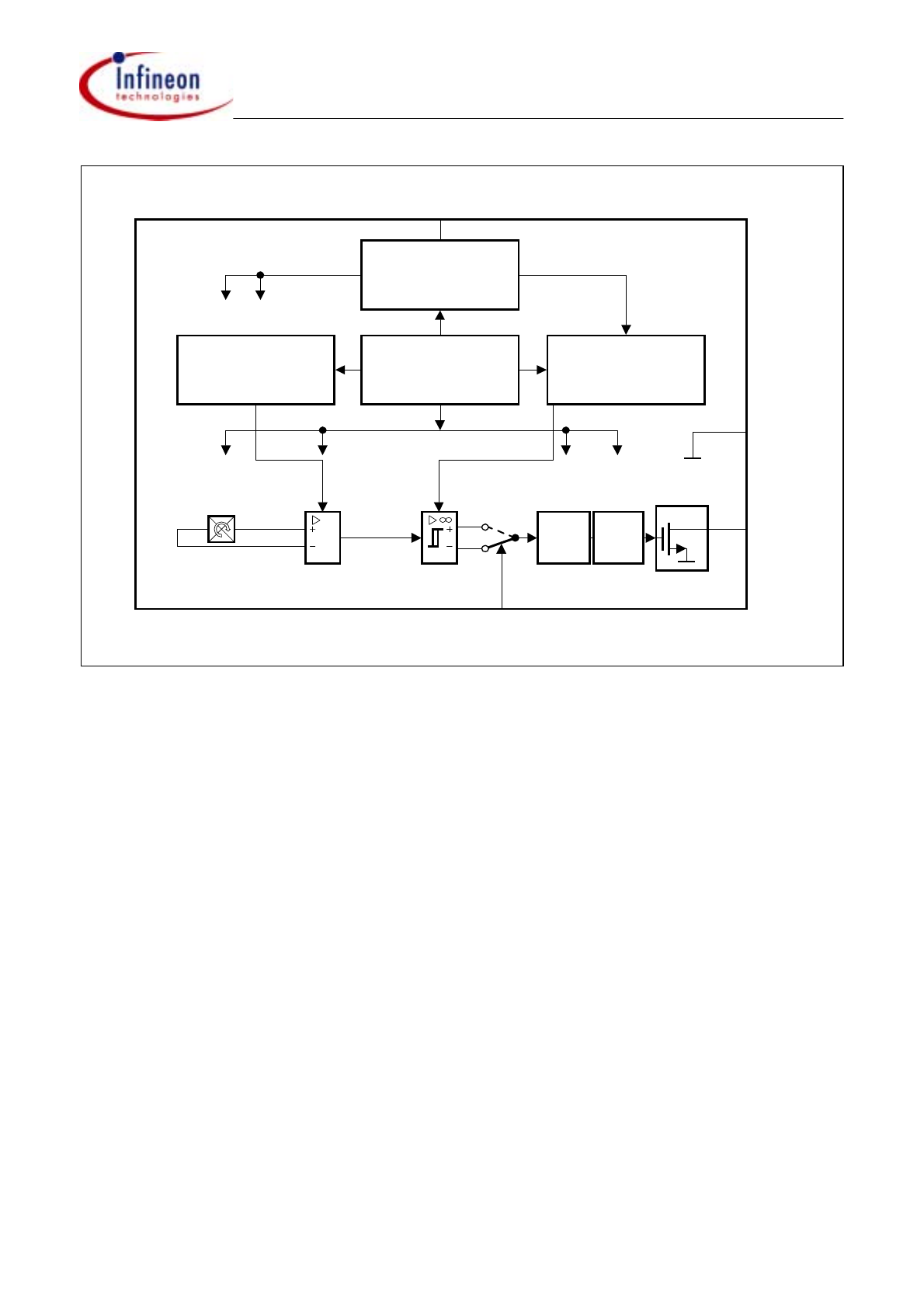
AEB02800_C
Chopped
Amplifier
Hall
Probe
Latch
Active Error
Compensation
Oscillator
&
Sequencer
Threshold
Generator
Bias and
Compensation
Circuits
V
S
1
2, 4, 5
GND
Comparator
with
Hysteresis
PRG
6
3 Q
Decision
Logic
Figure 2 Block Diagram
Circuit Description
The Low Power Hall IC Switch comprises a Hall probe, bias generator, compensation
circuits, oscillator, output latch and an n-channel open drain output transistor.
The bias generator provides currents for the Hall probe and the active circuits.
Compensation circuits stabilize the temperature behavior and reduce technology variations.
The Active Error Compensation rejects offsets in signal stages and the influence of
mechanical stress to the Hall probe caused by molding and soldering processes and other
thermal stresses in the package. This chopper technique together with the threshold
generator and the comparator ensures high accurate magnetic switching points.
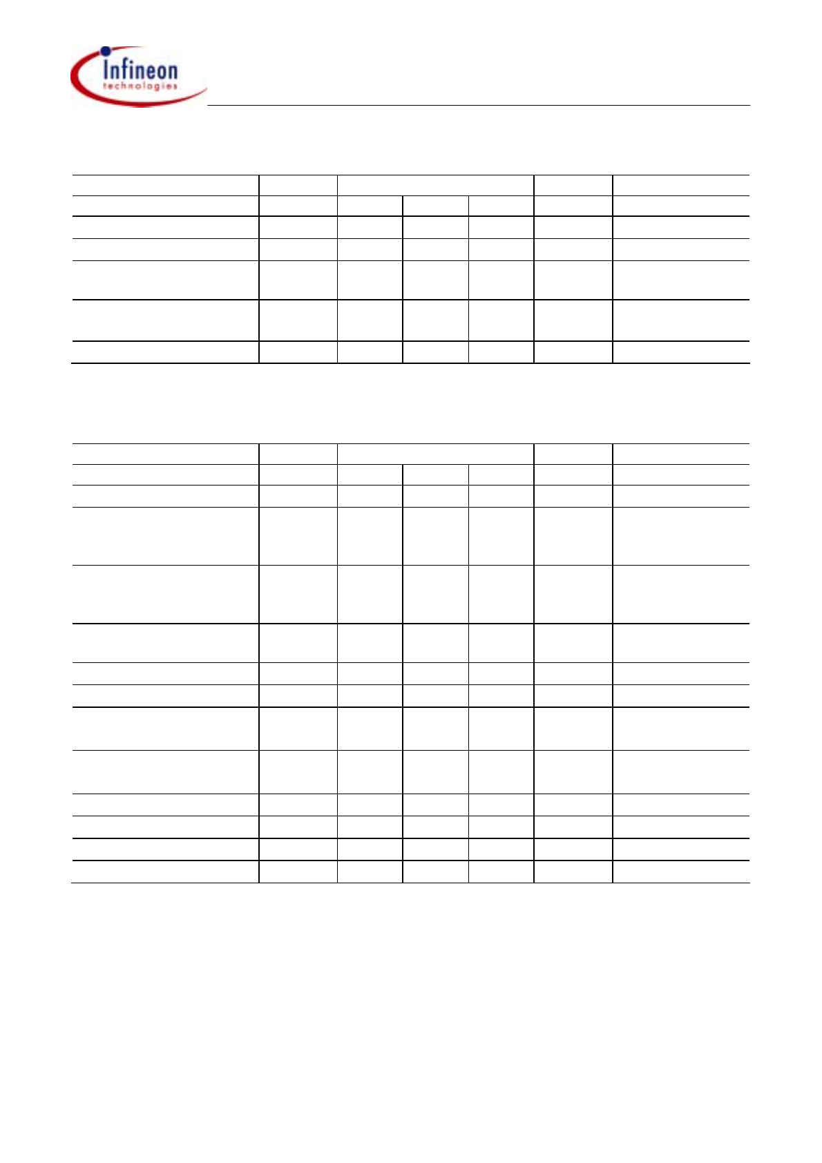
Very low power consumption is achieved with a timing scheme controlled by an oscillator
and a sequencer. This circuitry activates the sensor for 50 µs (typical operating time) sets
the output state after sequential questioning of the switch points and latches it with the
beginning of the following standby phase (typ. 130 ms). In the standby phase the average
current is reduced to typical 3.5 µA. Because of the long standby time compared to the
operating time the overall averaged current is only slightly higher than the standby current.
By connecting the programming pin to GND (normal to
V
S
) the Output State can be inverted
to further reduce the current consumption in applications where a high magnetic field is the
Data Sheet
4
normal state. In that case the output Q is off at high magnetic fields and no current is
flowing in the open drain transistor.
The output transistor can sink up to 1 mA with a maximal saturation voltage V
QSAT
.
Absolute Maximum Ratings
Parameter Symbol
Limit
Values
Unit
Notes
min. max.
Supply Voltage
V
S
– 0.3
5.5
V
Supply Current
I
S
– 1
2.5
mA
Output Voltage
V
Q
– 0.3
5.5
V
Output Current
I
Q
– 1
2
mA
Programming Pin Voltage
V
PRG
– 0.3
5.5
1)
V
Junction temperature
T
j
– 40
150
°C
Storage temperature
T
S
– 40
150
°C
Magnetic Flux Density
B
– unlimited
mT
Thermal Resistance
P-TSOP6-6-2
R
th JA
– 35
K/W
1)
V
PRG
must not exceed Vs by more than 0.3V
Note: Stresses above those listed here may cause permanent damage to the device.
Exposure to absolute maximum rating conditions for extended periods may affect
device reliability.
ESD Protection
Human Body Model (HBM) tests according to:
EOS/ESD Association Standard S5.1-1993 and Mil. Std. 883D method 3015.7
Parameter Symbol
Limit
Values
Unit
Notes
Min. max.
ESD Voltage
V
ESD
± 2
kV
R
= 1.5 k
Ω,
C
= 100 pF;
T
= 25 °C
Data Sheet
5
Operating Range
Parameter
Symbol Limit
Values
Unit
Notes
Min.
typ.
max.
Supply voltage
V
S
2.4 2.7 5.5 V
1)
Output voltage
V
Q
– 0.3
2.7
5.5
V
Programming Pin Voltage
V
PRG
– 0.3
0
0.3
V
Inverted output
state
V
S
–
0.3
V
S
V
S
+
0.3
Standard
output
state
Ambient Temperature
T
A
– 40
25
85
°C
1)
A Ceramic Bypass Capacitor of 10 nF at
V
S
to GND is highly recommended.
AC/DC Characteristics
Parameter
Symbol Limit
Values
Unit
Notes
Min.
typ.
Max.
Averaged Supply Current
I
SAVG
1 4 20 µA
Averaged Supply
Current
during Operating Time
I
SOPAVG
0.5 1.1 2.5 mA
Transient Peak Supply
Current
during Operating Time
I
SOPT
– – 2.5
mA
t
< 100 ns
Supply Current
during Standby Time
I
SSTB
1 3.5
20 µA
Output Saturation Voltage
V
QSAT
– 0.13
0.4
V
I
Q
= 1 mA
Output Leakage Current
I
QLEAK
– 0.01
1 µA
Output Rise Time
t
r
– 0.3
1 µs
R
L
= 2.7 k
Ω
;
C
L
= 10 pF
Output Fall Time
t
f
– 0.1
1 µs
R
L
= 2.7 k
Ω
;
C
L
= 10 pF
Operating Time
t
op
15 50 93
1) 2)
µs
Standby Time
t
stb
– 130
240
3)
ms
Duty Cycle
t
op
/
t
stb
– 0.039
– %
Start-up Time of IC
t
stu
– 6 12 µs
4)
1)
for V
S
=3.5V the max. Operating Time
t
op max
= 85µs
2)
includes the Start-up Time
t
stu
3)
for V
S
=3.5V the max. Standby Time
t
stb max
= 220ms
4)
initial power on time. V
S
must be applied in this time ( typ. 6µs to max. 12µs ) to get already a valid output
state after the first operating phase (typ. 56µs). For rise times of V
S
> 12µs, the output state is valid after the
second operating phase (includes one standby phase), e.g. happens only when the battery in flip phones is
changed.
Data Sheet
6
Magnetic Characteristics
PRG Pin Connected to V
S
Parameter
Symbol Limit
Values
Unit
Notes
Min.
typ.
max.
Operate Points
B
OPS
B
OPN
3.5
–7
5
–5
7
–3.5
mT
mT
1)
Release Points
B
RPS
B
RPN
2.2
–6
4
–4
6
–2.2
mT
mT
1)
Hysteresis B
HYS
0.2 1 2 mT
1)
Positive magnetic fields are related to the approach of a magnetic south pole to the branded side of package
PRG Pin Connected to GND
Parameter
Symbol Limit
Values
Unit
Notes
Min.
typ.
max.
Operate Points
B
OPS
B
OPN
2.2
-6
4
-4
6
-2.2
mT
mT
1)
Release Points
B
RPS
B
RPN
3.5
-7
5
-5
7
-3.5
mT
mT
1)
Hysteresis B
HY
0.2
1 2 mT
1)
Positive magnetic fields are related to the approach of a magnetic south pole to the branded side of package
Note: The listed AC/DC and magnetic characteristics are ensured over the operating range
of the integrated circuit. Typical characteristics specify mean values expected over
the production spread. If not other specified, typical characteristics apply at
T
j
= 25 °C
and
V
S
= 2.7 V.
Data Sheet
7
AET02802-17
I
S
t
I
SAVG
I
SSTB
Operating
Time
Standby Time
Latch
Output
t
op
50
µ
s
t
stb
130 ms
I
SOPAVG
Figure 3 Timing Diagram
Figure 4 Programming of Output with the PRG Pin
Data Sheet
8
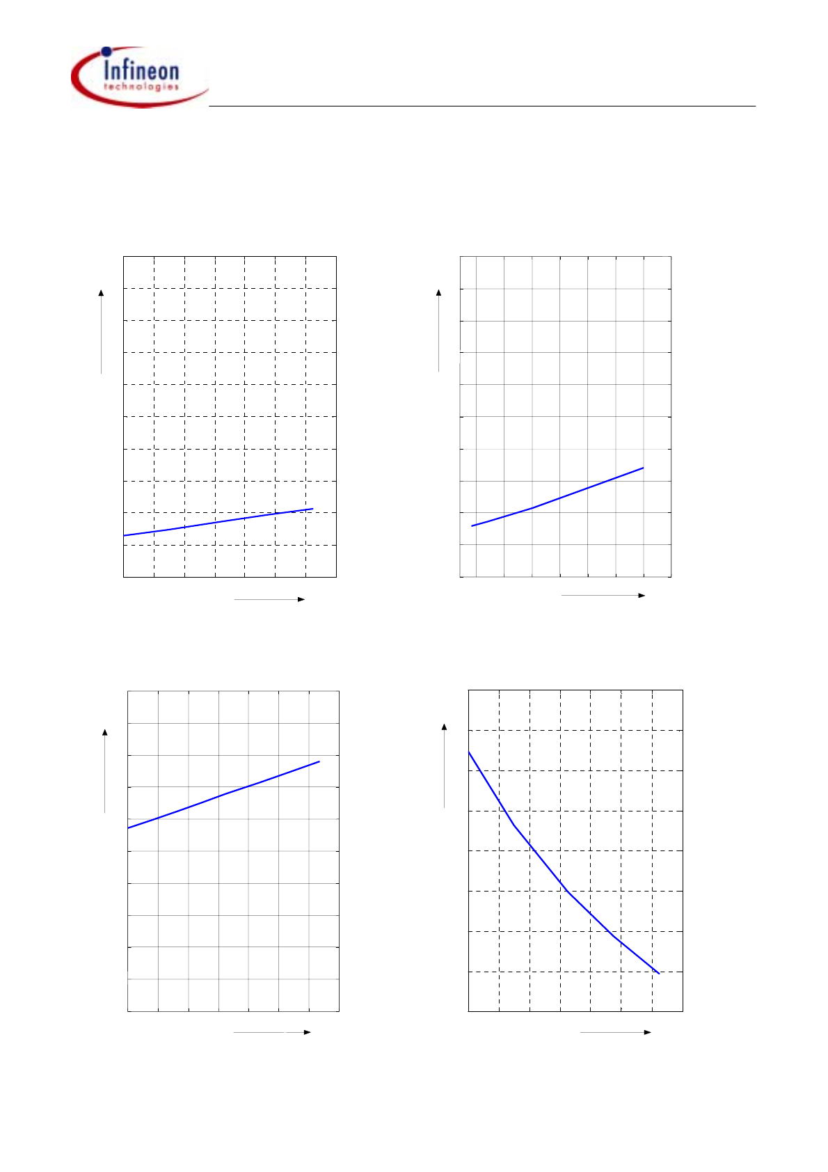
All curves reflect typical values at the given parameters for T
A
in
°
C and V
S
in V.
Magnetic Switching Points versus
Magnetic Switching Points versus
Temperature (V
S
=2.7V)
Supply
Voltage
V
S
(T
A
=20°C)
(PRG Pin Connected to V
S)
)
(PRG Pin Connected to V
S)
)
-40
-20
0
20
40
60
80
100
-6
-4
-2
0
2
4
6
B[mT]
T [°C]
B
OPS
RPS
B
B
RPN
OPN
B
2.5
3
3.5
4
4.5
5
5.5
6
-6
-4
-2
0
2
4
6
B[mT]
S
U [V]
B
OPS
RPS
B
B
RPN
OPN
B
Supply current I
SOPAVG
during Operating
Supply current I
SOPAVG
during Operating
Time versus Temperature (V
S
=2.7V)
Time versus Supply Voltage V
S
(T
A
=20°C)
-40
-20
0
20
40
60
80
100
0.5
1
1.5
2
2.5
I [mA]
T [°C]
SOPA V G
I
2.5
3
3.5
4
4.5
5
5.5
6
0
0.5
1
1.5
2
2.5
I [mA]
S
V [V]
SOPAVG
I
Data Sheet
9
Supply current I
SSTB
during Standby
Supply current I
SSTB
during Standby
Time versus Temperature (V
S
=2.7V)
Time versus Supply Voltage V
S
(T
A
=20°C)
-40
-20
0
20
40
60
80
100
0
2
4
6
8
10
12
14
16
18
20
I [µA]
T [°C]
SSTB
I
2.5
3
3.5
4
4.5
5
5.5
6
0
2
4
6
8
10
12
14
16
18
20
I [µA]
SSTB
I
S
V [V]
Output Saturation voltage V
QSAT
Standby Time t
stb
versus Temperature
versus Temperature ( I
Q
=1mA )
(V
S
= 2.7V)
-40
-20
0
20
40
60
80
100
0
20
40
60
80
100
120
140
160
200
V[mV]
V
QSAT
T [°C]
-40
-20
0
20
40
60
80
100
100
110
120
130
140
150
160
170
180
t
stb
t [ms]
T [°C ]
Data Sheet
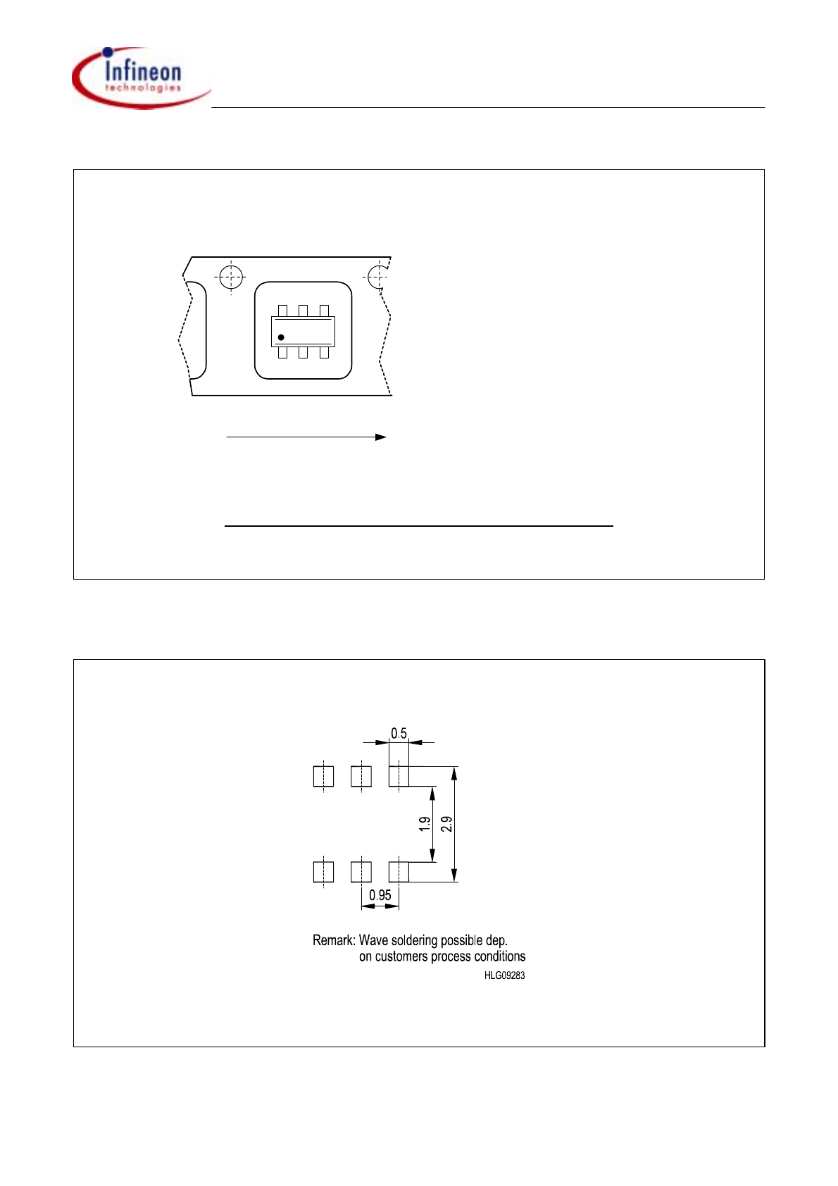
10
Top View
Marking on P-TSOP6-6-2 package
corresponds to pin 1 of device
17
6 5 4
1 2 3
Direction of Unreeling
S
y
m
Package
Pieces / Reel
∅
Reel
P-TSOP6-6-2
3.000
180 mm
Figure 5 Marking and Tape Loading Orientation
Figure 6 Foot Print Reflow Soldering