
www.irf.com
3-Jul-09
© 2009 International Rectifier
Data Sheet No. PD 60321A
IRS26302DJPBF
FULLY PROTECTED 3-PHASE BRIDGE PLUS ONE GATE
DRIVER
Features
•
Floating channel designed for bootstrap operation, fully
• operational to +600 V
•
Tolerant to negative transient voltage – dV/dt immune
•
Full three phase gate driver plus one low side driver
•
Undervoltage lockout for all channels
•
Cross-conduction prevention logic
•
Power-on reset
•
Integrated bootstrap diode for floating channel supply
•
Over current protection on: DC-(Itrip), DC+(Ground fault),
PFCtrip/BRtrip (PFC/Brake protection).
•
Single pin fault diagnostic function
•
Diagnostic protocol to address fault register
•
Self biasing for ground fault detection high voltage circuit
•
3.3 V logic compatible
•
Lower di/dt gate drive for better noise immunity
•
Externally programmable delay for automatic fault clear
•
RoHS compliant
Typical Applications
•
Air conditioners inverters
•
Micro/Mini inverter drives
•
General purpose inverter
•
Motor control
Product Summary
Topology
3 Phase
V
OFFSET
≤ 600 V
V
OUT
10 V – 20 V
I
o+
& I
o-
(typical)
200 mA & 350 mA
Deadtime (typical)
290 ns
Package
44-Lead PLCC
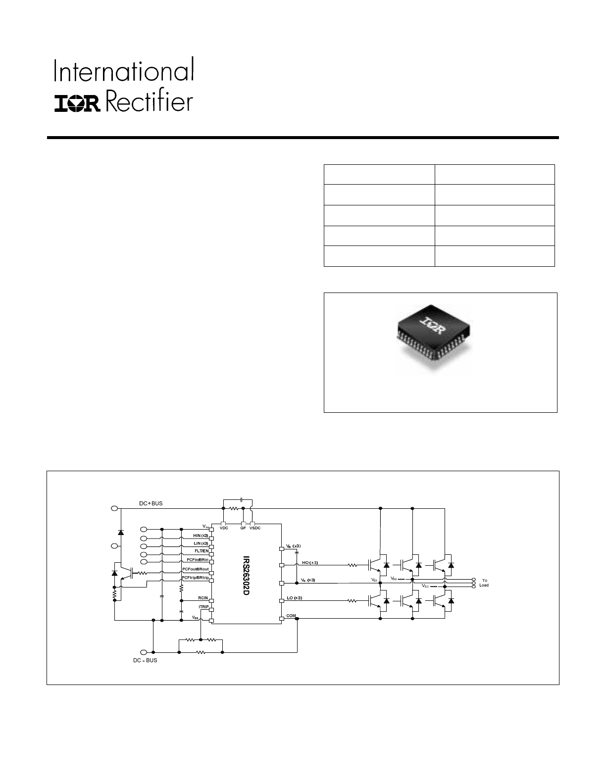
Typical Connection Diagram

IRS26302DJ
www.irf.com
© 2009 International Rectifier
2
Table of Contents
Page
Description
3
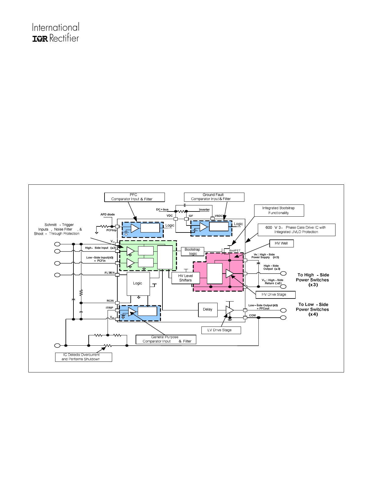
Simplified Block Diagram
3
Typical Application Diagram
4
Qualification Information
5
Absolute Maximum Ratings
6
Recommended Operating Conditions
7
Static Electrical Characteristics
8
Dynamic Electrical Characteristics
10
Functional Block Diagram
12
Input/Output Pin Equivalent Circuit Diagram
13
Lead Definitions
14
Lead Assignments
15
Application Information and Additional Details
16
Parameter Temperature Trends
36
Package Details
49
Tape and Reel Details
50
Part Marking Information
51
Ordering Information
52
IRS26302DJ
www.irf.com
© 2009 International Rectifier
3
Description
The IRS26302DJPBF are high voltage, high speed power MOSFET and IGBT drivers with three independent high
and low side referenced output channels for 3-phase applications. An additional low side driver is included for PFC
or Brake IGBT driving operation. Proprietary HVIC technology enables rugged monolithic construction. Logic inputs
are compatible with CMOS or LSTTL outputs, down to 3.3V logic. Three current trip functions that terminate all
seven outputs can be derived from three external shunt resistors. Each overcurrent trip functions consists of
detecting excess current across a shunt resistor on DC+ bus, on DC- bus and on Brake or PFC circuitry. An enable
function is available to terminate all outputs simultaneously and is provided through a bidirectional pin combined
with an open-drain FAULT pin. Fault signal is provided to indicate that an overcurrent or undervoltage shutdown
has occurred. Overcurrent fault conditions are cleared automatically after an externally programmed delay via an
RC network connected to the RCIN input. A diagnostic feature can give back to the controller the fault cause
(UVcc, DC- or DC- overcurrent) and address a fault register. The output drivers feature a high pulse current buffer
stage. Propagation delays are matched to simplify use in high frequency applications designed for minimum driver
cross conduction. The floating channel can be used to drive N-channel power MOSFET’s or IGBT’s in the high
side configuration which operates up to 600 V.
Simplified Block Diagram
IRS26302DJ
www.irf.com
© 2009 International Rectifier
4
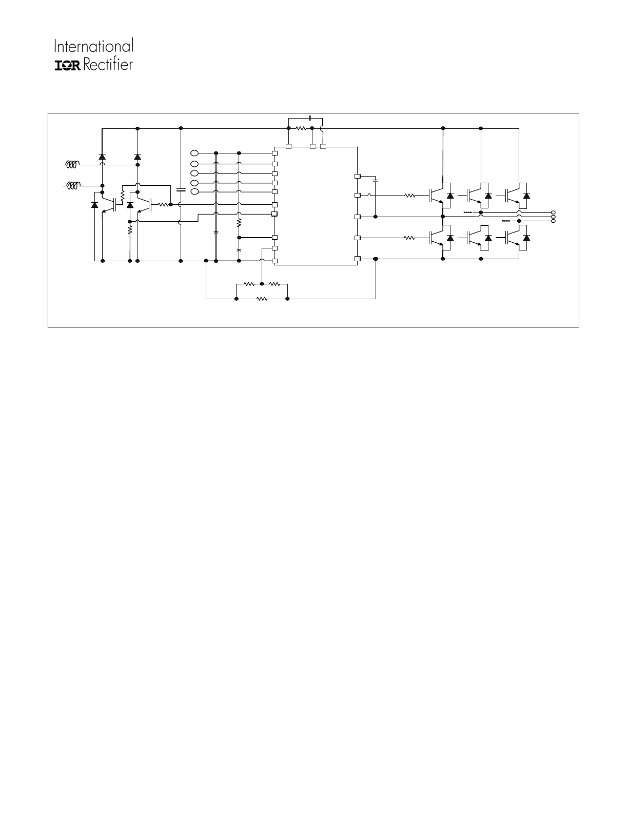
Typical Application Diagram
V
cc
HIN (x3)
RCIN
FLT/EN
ITRIP
V
SS
COM
LIN (x3)
LO (x 3)
HO ( x 3)
V
B
( x3 )
V
S
(x 3)
IR
S
2
6
3
0
2
D
V
S1
V
S2
V
S 3
DC+ BUS
DC - BUS
To
Load
VDC
GF
VSDC
PCFin/BRin
PCFout/BRout
PCFtrip/BRtrip
AC
main
IRS26302DJ
www.irf.com
© 2009 International Rectifier
5
Qualification Information
†
Industrial
††
(per JEDEC JESD 47E)
Qualification Level
Comments: This family of ICs has passed JEDEC’s
Industrial qualification. IR’s Consumer qualification level is
granted by extension of the higher Industrial level.
Moisture Sensitivity Level
PLCC44
MSL3
†††
(per IPC/JEDEC J-STD-020C)
Machine Model
Class B
(per JEDEC standard JESD22-A114D)
Human Body Model
Class 2
(per EIA/JEDEC standard EIA/JESD22-A115-A)
ESD
Charged Device Model
Class IV
(per JEDEC standard JESD22-C101C)
IC Latch-Up Test
Class I, Level A
(per JESD78A)
RoHS Compliant
Yes
†
Qualification standards can be found at International Rectifier’s web site
http://www.irf.com/
†† Higher qualification ratings may be available should the user have such requirements. Please contact your
International Rectifier sales representative for further information.
††† Higher MSL ratings may be available for the specific package types listed here. Please contact your
International Rectifier sales representative for further information.
IRS26302DJ
www.irf.com
© 2009 International Rectifier
6
Absolute Maximum Ratings
Absolute maximum ratings indicate sustained limits beyond which damage to the device may occur. All voltage
parameters are absolute voltages referenced to V
SS
unless otherwise stated in the table. The thermal resistance and
power dissipation ratings are measured under board mounted and still air conditions. Voltage clamps are included
between V
CC
& COM (25 V), V
CC
& V
SS
(20 V), and V
B
& V
S
(20 V).
Symbol
Definition
Min.
Max.
Units
V
B1,2,3
High side floating supply voltage
-0.3
620
V
HO1,2,3
High side floating output voltage
V
S1,2,3
- 0.3
V
B1,2,3
+ 0.3
V
S1,2,3
High side offset voltage
V
B1,2,3
- 20
V
B 1,2,3
+ 0.3
VDC
DCbus Supply Voltage
-0.3
620
GF
Input voltage for Ground Fault detection
VDC-20
VDC+0.3
VSDC
High voltage return for Ground Fault circuit
VDC-20
VDC+0.3
V
CC
Low side and logic fixed supply voltage
-0.3
20
†
COM
Power ground
V
CC
- 25
V
CC
+ 0.3
V
LO1,2,3
Low side output voltage LO1,2,3, PFCout
-0.3
V
CC
+ 0.3
V
IN
Input voltage LIN1,2,3, HIN1,2,3, ITRIP, PFCtrip,
FLTEN, RCIN
-0.3
V
CC
+ 0.3
V
PFCtrip
/V
BRtrip
Input voltage V
PFCtrip
/V
BRtrip
-2
V
CC
+ 0.3
V
dV/dt
Allowable offset voltage slew rate
—
50
V/ns
P
D
Package power dissipation @ TA ≤ +25°C
—
4.6
W
R
THJA
Thermal resistance, junction to ambient
—
27
°C/W
T
J
Junction temperature
—
150
T
S
Storage temperature
-55
150
T
L
Lead temperature (soldering, 10 seconds)
—
300
°C
†
All supplies are fully tested at 25 V. An internal 20 V clamp exists for each supply.
IRS26302DJ
www.irf.com
© 2009 International Rectifier
7
Recommended Operating Conditions
For proper operation, the device should be used within the recommended conditions. All voltage parameters are
absolute voltages referenced to V
SS
unless otherwise stated in the table. The offset rating is tested with supplies of
(V
CC
-COM) = (V
B
-V
S
) = 15 V. For proper operation the device should be used within the recommended conditions.
Symbol
Definition
Min.
Max.
Units
V
B1,2,3
High side floating supply voltage
V
S1,2,3
+ 10
V
S1,2,3
+ 20
V
HO 1,2,3
High side output voltage HO1,2,3
V
S1,2,3
V
B1,2,3
V
S 1,2,3
High side floating supply voltage
†
Vss – 8
600
V
St 1,2,3
Transient high side floating supply voltage
††
-50
600
VDC
DCbus Supply Voltage
(TBD)
600
GF
Input voltage for Ground Fault detection
VDC-5
VDC
VSDC
High voltage return for Ground Fault circuit
VDC-12
VDC-11
V
CC
Low side supply voltage
10
20
V
LO1,2,3
Low side output voltage LO1,2,3, PFCout
0
V
CC
COM
Power ground
-5
5
V
SCOM
Negative transient Vs voltage
0
-20
1)
V
FLT
FAULT output voltage
0
V
CC
V
RCIN
RCIN input voltage
0
V
CC
V
HO 1,2,3
High side output voltage
V
S1,2,3
V
B1,2,3
V
LO1,2,3
Low side output voltage
COM
V
CC
V
ITRIP
ITRIP input voltage
0
5
PFC
ITRIP
/BR
ITRIP
PFC
ITRIP
/BR
ITRIP
input voltage
-2
0
V
IN
Logic input voltage LIN, HIN, PFCin, BRin, EN
V
SS
V
SS
+5
V
T
A
Ambient temperature
-40
125
ºC
†
Logic operation for V
S
of –8 V to 600 V. Logic state held for V
S
of –8 V to –V
BS
. Please refer to Design Tip
DT97-3 for more details.
†† Operational for transient negative V
S
of V
SS
- 50 V
with a 50 ns pulse width. Guaranteed by design. Refer to
the Application Information section of this datasheet for more details.
IRS26302DJ
www.irf.com
© 2009 International Rectifier
8
Static Electrical Characteristics
(V
CC
-COM) = (V
B
-V
S
) = 15 V. TA = 25
°C
unless otherwise specified. The VIN and IIN parameters are referenced
to V
SS
and are applicable to all six channels. The VO and IO parameters are referenced to respective V
S
and
COM and are applicable to the respective output leads HO or LO. The V
CCUV
parameters are referenced to V
SS
.
The V
BSUV
parameters are referenced to V
S
. The PFCIo/BRIo and VPFC/ VBR are referenced to V
SS
and are
applicable to PFCout/BRout lead.
Symbol
Definition
Min
Typ
Max Units
Test Conditions
VIH
Logic “1” input voltage
2.5
—
—
VIL
Logic “0” input voltage
—
—
0.8
V
IN,TH+
Input positive going threshold
—
1.9
2.5
V
IN,TH-
Input negative going threshold
0.8
1
—
V
IT,TH+
Input positive going threshold
0.160
0.200
0.240
V
IT,TH-
Input negative going threshold
0.144
0.180
0.216
V
V
IT,HYS
ITRIP hysteresis
—
20
—
mV
V
PFCT,TH+
V
BRT,TH+
PFC/BR positive going threshold
-0.144 -0.180 -0.216
V
PFCT,TH-
V
BRT,TH-
PFC/BR negative going threshold
-0.160 -0.200 -0.240
V
V
PFCT,HYS
V
BRT,HYS
PFC/BR hysteresis
—
20
—
mV
V
GFT,TH+
GF positive going threshold
0.140
0.180
0.220
V
GFT,TH-
GF negative going threshold
0.150
0.200
0.240
V
V
GFT
= V
DC
- V
GF
V
GFT,HYS
GF hysteresis
—
20
—
mV
V
RCIN,TH+
RCIN positive going threshold
—
8
—
V
RCIN,HYS
RCIN hysteresis
—
3
—
V
CC,UVTH+
V
CC
supply undervoltage positive going
threshold
10.2
11.1
12.0
V
CC,UVTH-
V
CC
supply undervoltage negative going
threshold
10.0
10.9
11.8
V
CC,UVHYS
V
CC
supply undervoltage hysteresis
—
0.2
—
V
BS,UVTH+
V
BS
supply undervoltage positive going
threshold
10.2
11.1
12.0
V
BS, UVTH-
V
BS
supply undervoltage negative going
threshold
10.0
10.9
11.8
V
BS,UVHS
V
BS
supply undervoltage hysteresis
—
0.2
—
V
ILK
Offset supply leakage current
—
—
50
µA
VB1,2,3 = VDC = GF =600 V,
VDC - VDCS = 20 V
Iqbs
Quiescent VBS supply current
—
45
120
All input/output in off status
Iqcc
Quiescent VCC supply current
—
2.5
4
mA
All input/output in off status
Io+
Output high short circuit pulsed current,
HO1,2,3
100
200
—
Vout = 0 V, PW </= 10 us
Io-
Output low short circuit pulsed current,
HO1,2,3
190
350
—
mA
Vout = 15 V, PW </= 10 us
VOH
High level output voltage, VBIAS – VO,
HO1,2,3
—
0.9
1.4
V
IO = 20 mA
VOL
Low level output voltage, VO, HO1,2,3
—
0.4
0.6

IRS26302DJ
www.irf.com
© 2009 International Rectifier
9
Static Electrical Characteristics (continued)
(V
CC
-COM) = (V
B
-V
S
) = 15 V. TA = 25
°C
unless otherwise specified. The VIN and IIN parameters are referenced
to V
SS
and are applicable to all six channels. The VO and IO parameters are referenced to respective V
S
and
COM and are applicable to the respective output leads HO or LO. The V
CCUV
parameters are referenced to V
SS
.
The V
BSUV
parameters are referenced to V
S
. The PFCIo/BRIo and VPFC/ VBR are referenced to V
SS
and are
applicable to PFCout/BRout lead.
Symbol
Definition
Min
Typ
Max Units
Test Conditions
PFCI
O+
/
BRI
O+
Output high short circuit pulsed current,
PFC
OUT
/BR
OUT
120
250
—
P
FCOUT
= 0 V, PW </= 10 us
PFCI
O-
/
BRI
O-
Output low short circuit pulsed current,
PFC
OUT
/BR
OUT
210
430
—
mA
P
FCOUT
= 15 V, PW </= 10 us
V
PFCH
/V
BRH
High level output voltage, V
BIAS
– V
O
,
PFC
OUT
/BR
OUT
—
900
1400
V
PFCL
/V
BRL
low level output voltage, V
O
, PFC
OUT
/BR
OUT
—
400
600
mV
I
O
= 20 mA
I
IN+
Input bias current LIN1,2,3, HIN1,2,3,
PFC
IN
/BR
IN,
(OUT=HI)
350
—
860
V
IN
= 3.3 V
I
IN-
Input bias current LIN1,2,3, HIN1,2,3,
PFC
IN
/BR
IN,
(OUT=LO)
—
0
1
V
IN
= 0 V
I
ITRIP+
ITRIP input bias current
—
1
2
V
ITRIP
= 1 V
I
ITRIP-
ITRIP input bias current
—
0
5
V
ITRIP
= 0 V
IPFC
TRIP+
/
IBR
TRIP+
PFC
TRIP
/BR
TRIP
input bias current
—
20
—
V
PFCTRIP
=-250 mV
IPFC
TRIP
/
IBR
TRIP-
PFC
TRIP
/BR
TRIP
input bias current
—
0
5
V
PFCTRIP
= 0 V
I
RCIN
RCIN input bias current
—
0
5
V
RCIN
= 15 V
IEN
IN
EN input bias current
—
0
1
µA
V
EN
= 3.3V
Ron_RCIN
RCIN low on resistance
—
50
100
I = 1.5 mA
R
ON_FLT
FLT low on resistance
—
50
100
I = 1.5 mA
RBS
Ron internal bootstrap diode
—
200
—
Ω
IqVdcon
Quiescent VDC supply current on status
100
200
300
VDC - Vgf = 250 mV,
VDC+ = 40 -600 V
IqVdcoff
Quiescent VDC supply current off status
100
200
300
µA
VDC = Vgf , VDC + = 40- 600 V

IRS26302DJ
www.irf.com
© 2009 International Rectifier
10
Dynamic Electrical Characteristics
V
CC
= V
B
= 15 V, V
S
= V
SS
= COM, T
A
= 25
°C
, and C
L
= 1000 pF unless otherwise specified.
Symbol
Definition
Min
Typ
Max
Units
Test Conditions
LO
ton
,
HO
ton
Turn-on propagation delay, LO1,2,3,
HO1,2,3
320
—
710
LIN = 0 V ≥ 3.3 V, HIN = 0 V
LO
toff
,
HO
toff
Turn-off propagation delay, LO1,2,3,
HO1,2,3
320
—
710
LIN = 3.3 V ≥ 0 V, HIN = 0 V
LO
tr
, HO
tr
Turn-on rise time LO1,2,3, HO1,2,3
—
125
190
C
LOAD
= 1nF
LO
tf
,HO
tf
Turn-off fall time LO1,2,3, HO1,2,3
—
50
75
C
LOAD
= 1nF
P
FCton
/B
Rton
Turn-on propagation delay,
PFC
OUT
/BR
OUT
(CL = 2200pF)
300
—
660
P
FCIN
= 0 V ≥ 3.3 V
P
FCtoff
/B
Rtoff
Turn-off propagation delay,
PFC
OUT
/BR
OUT
(CL = 2200pF)
300
—
660
P
FCIN
= 3.3 V ≥ 0 V
P
FCtr
/B
Rtr
Turn-on rise time, PFC
OUT
/BR
OUT
(CL= 2200 pF)
—
180
—
C
LOAD
= 2.2 nF
P
FCtf
/B
Rtf
Turn-off rise time, PFC
OUT
/BR
OUT
(CL
= 2200 pF)
—
60
—
C
LOAD
= 2.2 nF
t
EN
ENABLE low to output shutdown
propagation delay
350
460
650
V
IN,
V
EN
= 0 V or 3.3 V
t
ITRIP
ITRIP to output shutdown propagation
delay
—
800
—
V
ITRIP
= 2 V
t
ITRIPbl
ITRIP blanking time
250
400
600
V
IN
= 0 V or 3.3 V
V
ITRIP
= 2 V
t
PFCtrip
PFC
TRIP
to output shutdown
propagation delay
—
800
—
t
PFCbl
/t
BRbl
PFC
TRIP
/BR
TRIP
blanking time
—
500
—
t
FILIN
Input filter time
†
(HIN, LIN, PFC
IN
/BR
IN
, EN)
200
350
—
V
IN
= 0 V & 3.3 V
t
filterEn
Enable input filter time
100
200
—
DT
Deadtime
190
290
420
LIN = 3.3 V ≥ 0 V, HIN = 0 V ≥
3.3 V
MT
Ton, off matching time (on all six
channels)
—
—
50
MDT
DT matching (Hi->Lo & Lo->Hi on all
channels)
—
—
60
PM
Pulse width distortion
††
—
—
75
ns
PW input = 10 us
t
FLTCLR
FAULT clear time RCIN: R=2meg,
C=1nF
40
60
80
µs
R = 100 KΩ, C = 680 pF, on
RCIN
t
ITRIPBLK
ITRIP blanking time
250
400
600
t
ITRIPFLT
ITRIP to fault time
800
1150
1500
V
ITRIP
= 0 V ≥ 2 V to FLT/En =
3.3 V ≥ 0 V
t
ITRIPOUT
ITRIP to output shutdown propagation
delay
500
720
950
ns
V
ITRIP
=0 V ≥ 2 V to LOx/Hox =
15 V ≥ 0 V
†
The minimum width of the input pulse is recommended to exceed 500 ns to ensure the filtering time of the
input filter is exceeded.
†† PM is defined as PW
IN
- PW
OUT
.