
www.irf.com
© 2009 International Rectifier
23
July 7, 2009
IRS2552D
CCFL/EEFL BALLAST CONTROLLER IC
Features
• Drives up to two IGBT/MOSFET power devices
• Integrated programmable oscillator
• Soft start function
• 15.6 V voltage clamp on V
CC
• Micro-power startup
• 0 V to 5 V input analog dimming
• Programmable ignition frequency
• Programmable ignition time
• Lamp current control
• Programmable
deadtime
• Supports multi-lamp operation
• Burst dimming with soft start at every burst
• Latched open circuit protection
• Integrated bootstrap functionality
• Excellent latch immunity on all inputs & outputs
• Integrated ESD protection on all pins
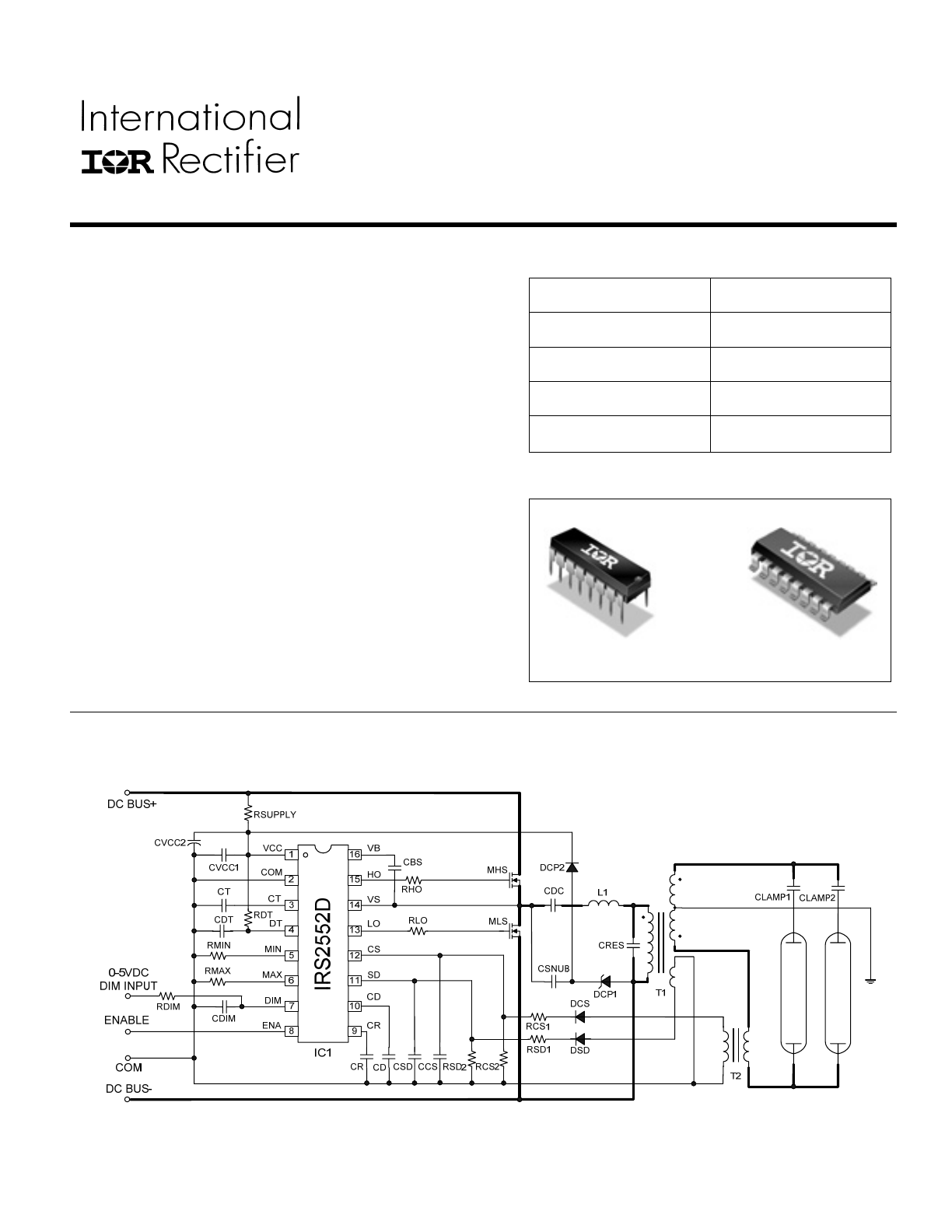
Typical Application
• CCFL/EEFL
inverter
Product Summary
Topology Half-Bridge
V
OFFSET
600 V
V
OUT
V
CC
I
O+
& I
O-
(typical)
300 mA & 450 mA
Deadtime
(programmable)
500ns ~ 2µs
Package Options
16-Lead PDIP
16-Lead SOIC (Narrow Body)
Typical Application Diagram
IRS2552D
www.irf.com
© 2009 International Rectifier
2
Table of Contents
Page
Typical Application Diagram
1
Qualification Information
4
Absolute Maximum Ratings
5
Recommended Operating Conditions
6
Electrical Characteristics
7
Functional Block Diagram
10
Lead Definitions
12
Lead Assignments
13
State Diagram
14
Application Information and Additional Details
15
Package Details
29
Part Marking Information
30
Ordering Information
32

IRS2552D
www.irf.com
© 2009 International Rectifier
3
Description
The IRS2552D incorporates a high voltage half-bridge gate driver with a front end that incorporates full control
functionality for CCFL/EEFL ballasts. Includes a programmable ignition and supports dimming via analog or PWM
control voltage. HVIC and latch immune CMOS technologies enable ruggedized monolithic construction. The
output driver features a high pulse current buffer stage designed for minimum driver cross-conduction. Noise
immunity is achieved with low di/dt peak of the gate drivers, and with an undervoltage lockout hysteresis of
approximately 1 V. The IRS2552D also includes protection features for over-current and over-voltage of the lamps.
IRS2552D
www.irf.com
© 2009 International Rectifier
4
Qualification Information
†
Industrial
††
(per JEDEC JESD 47E)
Qualification Level
Comments: This family of ICs has passed JEDEC’s
Industrial qualification. IR’s Consumer qualification level is
granted by extension of the higher Industrial level.
SOIC16
MSL3
†††
(per IPC/JEDEC J-STD-020C)
Moisture Sensitivity Level
PDIP16
Not applicable
(non-surface mount package style)
Machine Model
Class C
(per JEDEC standard EIA/JESD22-A115-A)
ESD
Human Body Model
Class 3A
(per EIA/JEDEC standard JESD22-A114-B)
IC Latch-Up Test
Class I, Level A
(per JESD78A)
RoHS Compliant
Yes
†
Qualification standards can be found at International Rectifier’s web site
http://www.irf.com/
†† Higher qualification ratings may be available should the user have such requirements. Please contact your
International Rectifier sales representative for further information.
††† Higher MSL ratings may be available for the specific package types listed here. Please contact your
International Rectifier sales representative for further information.
IRS2552D
www.irf.com
© 2009 International Rectifier
5
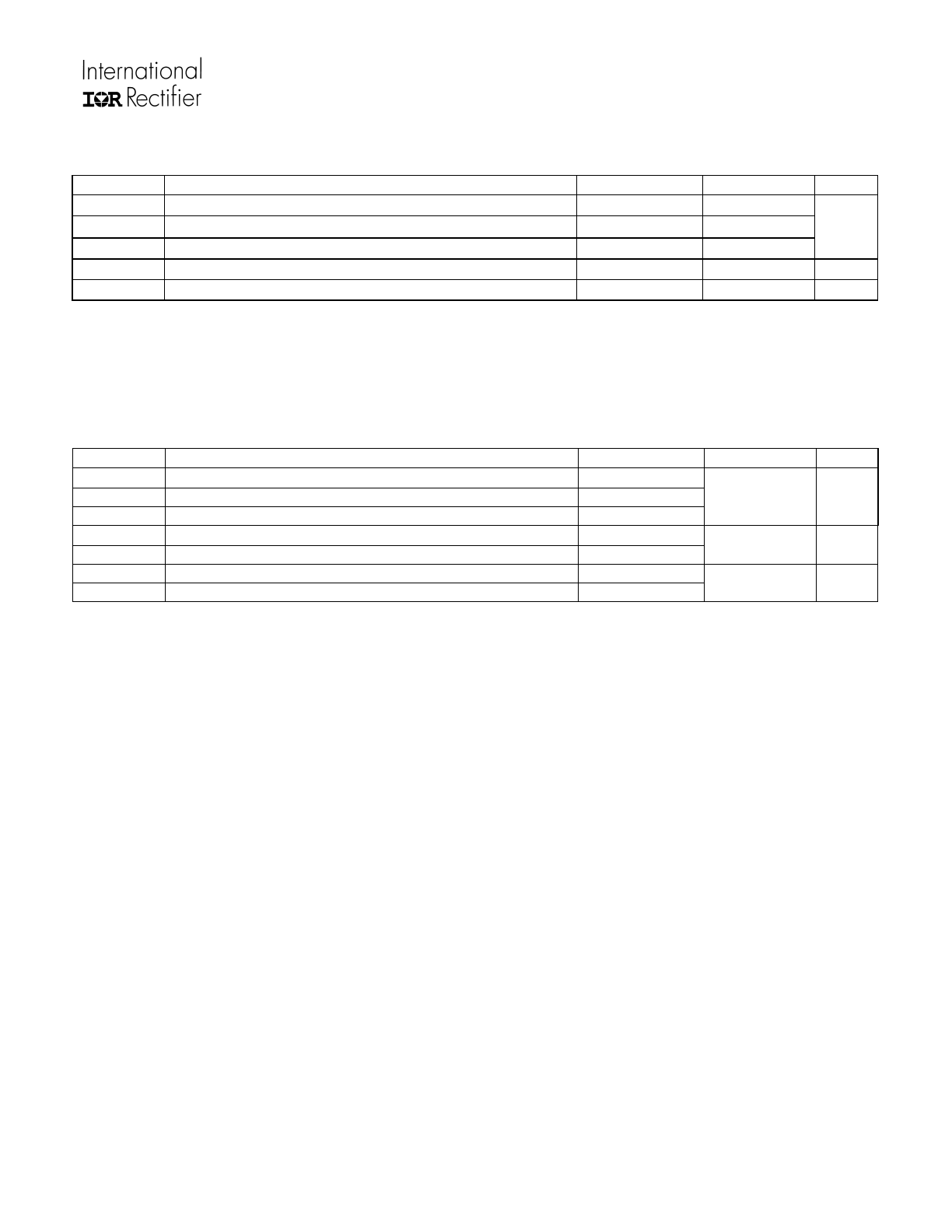
Absolute Maximum Ratings
Absolute maximum ratings indicate sustained limits beyond which damage to the device may occur. All voltage
parameters are absolute voltages referenced to COM, all currents are defined positive into any lead. The thermal
resistance and power dissipation ratings are measured under board mounted and still air conditions.
Symbol Definition
Min.
Max.
Units
V
B
High-side floating supply voltage
-0.3
625
V
S
High-side floating supply offset voltage
V
B
- 25
V
B
+ 0.3
V
H
High-side floating output voltage
V
S
– 0.3
V
B
+ 0.3
V
L
Low-side output voltage
-0.3
V
CC
+ 0.3
V
CO
VCO pin voltage
-0.3
V
CC
+ 0.3
V
CT
CT pin voltage
-0.3
V
CC
+ 0.3
V
DT
DT pin voltage
-0.3
V
CC
+ 0.3
MIN
MIN pin voltage
-0.3
V
CC
+ 0.3
DIM
DIM pin voltage
-0.3
V
CC
+ 0.3
CR
CR pin voltage
-0.3
V
CC
+ 0.3
CD
CD pin voltage
-0.3
V
CC
+ 0.3
SD
SD pin voltage
-0.3
V
CC
+ 0.3
CS
CS pin voltage
-0.3
V
CC
+ 0.3
V
I
CC
Supply current
†
--- 25
mA
dV
S
/dt
Allowable offset voltage slew rate
-50
50
V/ns
16L-PDIP --- 1.3
P
D
Package power dissipation @ T
A
≤ +25
ºC
16L-SOIC --- 1.4
W
16L-PDIP --- 70
R
ΘJA
Thermal resistance, junction to ambient
16L-SOIC --- 82
ºC/W
T
J
Junction temperature
-55
150
T
S
Storage temperature
-55
150
T
L
Lead temperature (soldering, 10 seconds)
---
300
ºC
† This IC contains a voltage clamp structure between the chip V
CC
and COM which has a nominal breakdown
voltage of 15.6 V. Please note that this supply pin should not be driven by a DC, low impedance power source
greater than the V
CLAMP
specified in the Electrical Characteristics section.
IRS2552D
www.irf.com
© 2009 International Rectifier
6
Recommended Operating Conditions
For proper operation the device should be used within the recommended conditions.
Symbol Definition
Min.
Max.
Units
V
BS
High-side floating supply voltage
V
CC
– 0.7
V
CLAMP
V
S
Steady-state high-side floating supply offset voltage
-3.0
†
600
V
CC
Supply voltage
V
CCUV+
+0.1V
V
CLAMP
V
I
CC
Supply current
††
10 mA
T
J
Junction temperature
-40
125
ºC
† Care should be taken to avoid output switching conditions where the VS node flies inductively below ground
by more than 5 V.
†† Enough current should be supplied to the V
CC
pin of the IC to keep the internal 15.6 V zener diode clamping
the voltage at this pin.
Recommended Component Values
Symbol Component
Min.
Max.
Units
R
MIN
MIN pin resistor value
5
R
MAX
MAX pin resistor value
5
R
DT
DT pin resistor value
22
---
k
Ω
C
T
CT pin capacitor value
330
C
DT
DT pin capacitor value
47
--- pF
C
R
CR pin capacitor value
1
C
D
CD pin capacitor value
1
--- nF
IRS2552D
www.irf.com
© 2009 International Rectifier
7
Electrical Characteristics
V
BIAS
(V
CC
, V
BS
) = 14 V, C
T
= 1 nF and T
A
= 25 °C unless otherwise specified. The input parameters are referenced to
COM. The V
O
and I
O
parameters are referenced to COM and are applicable to the respective output leads: HO or
LO.
Symbol Definition Min
Typ
Max
Units
Test
Conditions
Low Voltage Supply Characteristics
V
CCUV+
Rising
V
CC
undervoltage lockout threshold
9.5 10.5 11.5
V
CCUV-
Falling
V
CC
undervoltage lockout threshold
8.5 9.5 10.5
V
CCUVHYS
V
CC
undervoltage lockout hysteresis
0.5 1 1.5
V N/A
I
QCCUV
Micropower startup V
CC
supply current
--- 300 350 µA
V
CC
= V
CCUV+
-100 mV rising
I
QCC
Quiescent V
CC
supply current
--- 4.0 4.5
R
MIN
= 12 kΩ, RUN
MODE CT = 0 V
I
QCCFLT
V
CC
supply current
--- 0.9 1.3
Fault
mode
I
CC,FMIN
V
CC
current @ f
osc
= fMIN
--- 4.7 5.3
mA
R
MIN
= 12 k
Ω, RUN
MODE
V
CLAMP
V
CC
clamp voltage
14.6 15.6 16.6 V
I
CC
= 19 mA
Floating Supply Characteristics
I
QBSUV
Micropower startup V
BS
supply current
--- 6 20
V
CC
≤ V
CCUV-
,
V
CC
= V
BS
I
BS
V
BS
supply current
--- 1000
1200
µA
HO oscillating
V
BSUV+
V
BS
supply undervoltage positive going
threshold
6.5 7.5 8.5
V
BSUV-
V
BS
supply undervoltage negative going
threshold
6.0 7.0 8.0
V N/A
I
LK
Offset supply leakage current
--- --- 50
μA
V
B
= V
S
= 600 V
Oscillator I/O Characteristics
f
MIN
Minimum oscillator frequency
36.5
39
42.5
R
MIN
= 12 k
Ω, RUN
MODE
f
MAX
Maximum oscillator frequency
67
69
71
kHz
R
MAX
= 6.8 k
Ω,
IGNITION MODE
V
CT+
Upper CT ramp voltage threshold
4.8
5.0
5.2
V
CT-
Lower CT ramp voltage threshold
---
0
---
V N/A
I
CT
CT pin source current
350
410
470
μA
R
MIN
=12 k
Ω, RUN
MODE
V
MIN
VMIN pin voltage
4.8
5.0
5.2
V
MAX
VMAX pin voltage
4.8
5.0
5.2
V
MIN,FLT
VMIN voltage in fault mode
---
0
---
V
MAX,FLT
VMAX voltage in fault mode
---
0
---
V N/A
IRS2552D
www.irf.com
© 2009 International Rectifier
8
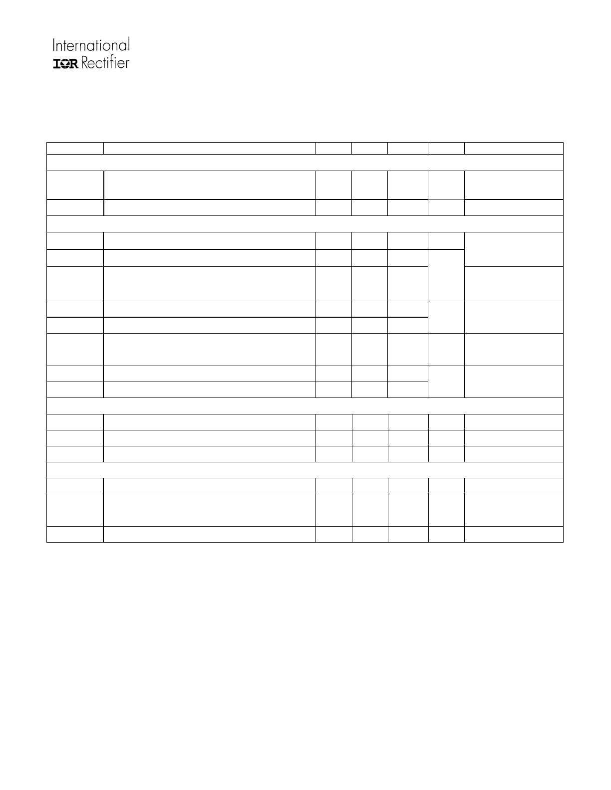
Electrical Characteristics
V
BIAS
(V
CC
, V
BS
) = 14 V, C
T
= 1 nF and T
A
= 25 °C unless otherwise specified. The input parameters are referenced to
COM. The V
O
and I
O
parameters are referenced to COM and are applicable to the respective output leads: HO or
LO.
Symbol Definition Min
Typ
Max
Units
Test
Conditions
Ignition
I
CR,IGN
Source current at CR pin in IGN mode
3.7
4.5
5.3
μA
R
MIN
= 12 k
Ω,
IGNITION MODE
V
CS,IGN
Ignition detection threshold
0.57
0.6
0.63
V
N/A
Gate Driver Output Characteristics
V
OH
High-level output voltage, V
BIAS
– V
O
--- V
CC
--- V
V
OL
Low-level output voltage, VO
--- COM ---
I
O
= 0 A
V
OL,UV
UV-mode output voltage, VO
--- COM ---
mV
I
O
= 0 A,
V
CC
≤ V
CCUV-
t
R
Output rise time
---
80
150
t
F
Output fall time
---
45
100
ns N/A
t
D
Output deadtime (HO or LO)
1.0
1.1
1.2
μs
R
DT
= 2.2 k
Ω,
C
DT
= 1 nF
I
O+
Output source current
---
300
---
I
O-
Output sink current
---
450
---
mA N/A
Bootstrap FET Characteristics
V
B,ON
V
B
when the bootstrap FET is on
13.2
13.5
---
V
N/A
I
B,CAP
V
B
source current when FET is on
40
55
---
mA
C
BS
= 0.1 μF
I
B,10V
V
B
source current when FET is on
9
12
---
mA
V
B
= 10 V
Shutdown
V
SD
,
TH
Shutdown threshold at SD pin
1.9
2.0
2.1
V
N/A
I
CD,source
CD pin source current
3.7
4.5
5.3
μA
V
SD
>V
SD,TH
,
R
MIN
= 12 k
Ω
V
CD,TH
Threshold at which CD triggers shutdown
4.8
5.0
5.2
V
V
CC
= 14 V
IRS2552D
www.irf.com
© 2009 International Rectifier
9
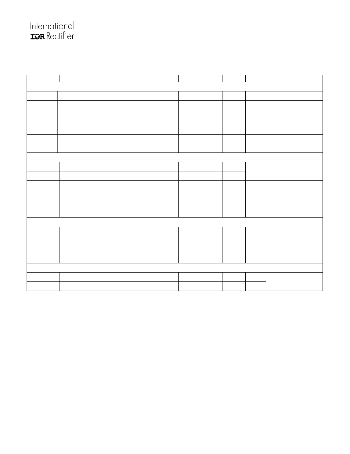
Electrical Characteristics
V
BIAS
(V
CC
, V
BS
) = 14 V, C
T
= 1 nF and T
A
= 25 °C unless otherwise specified. The input parameters are
referenced to COM. The V
O
and I
O
parameters are referenced to COM and are applicable to the respective
output leads: HO or LO.
Symbol Definition Min
Typ
Max
Units
Test
Conditions
Over-Current Compensation
V
CS,TH
Current compensation threshold at CS pin
1.15
1.21
1.27
V
N/A
I
CD,OC
Source current at CD pin when the IC is in
current compensation mode
3.7 4.5 5.3
μA
V
CS
>V
CS,TH
,
R
MIN
= 12 k
Ω
V
CD,oc
Voltage on CD where duty cycle reaches
minimum
4.8 5.0 5.2 V
N/A
DC
MIN
Minimum HO duty cycle
---
10%
---
---
V
CD
= 4.7 V,
RUN MODE
Dimming
V
CR+
CR pin upper threshold voltage
4.8
5.0
5.2
V
CR-
CR pin lower threshold voltage
---
0.2
---
V N/A
I
CR,RUN
Source current at CR pin in RUN mode
125
150
175
μA R
MIN
= 12 k
Ω
f
CR
Frequency at CR pin
240
310
370
Hz
C
R
= 100 nF,
RUN MODE,
R
MIN
= 12 k
Ω
Soft Start
DC
MIN
Minimum HO duty cycle
---
10%
---
---
V
CR
= 0 V,
V
DIM
< V
DIM,SS
V
CR,SS
End of soft start voltage
0.88
0.96
1.04
V
DIM
< V
DIM,SS
V
DIM,SS
Soft start disable threshold
---
4.8
---
V
N/A
Enable
V
ENATH
Enable
threshold
1.9 2.2 2.5 V
V
ENAHYS
Enable
hysteresis
--- 200 --- mV
N/A
IRS2552D
www.irf.com
© 2009 International Rectifier
10
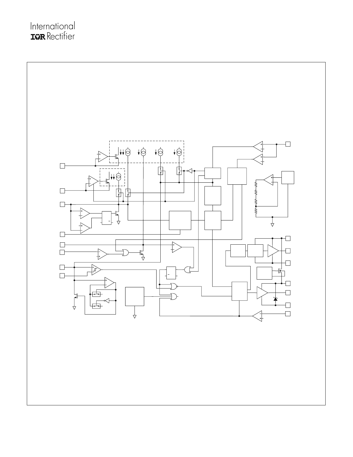
Functional Block Diagram
Q
S
R
Q
3
CT
8
ENA
11
SD
6
MAX
7
DIM
12
CS
5
MIN
0.6V
4
DT
10
CD
9
CR
Q
S
R2 Q
R1
IMIN
5V
5V
0V
ICD
2.2V
2V
1.21V
UV
5V
IMAX
UVLO
UV
0.2V
5V
ICR_IGN
ICR_RUN
BAND
GAP
REF
5V
VBG
IGNITION
LOGIC
SOFT
START
CONTROL
OVER
CURRENT
CONTROL
DEAD TIME
CONTROL
DUTY
CYCLE
CONTROL
OUTPUT
LOGIC
1
13
2
COM
LO
VCC
15.6V
15
16
14
VS
HO
VB
LEVEL
SHIFT
PULSE
FILTER &
LATCH
BOOT
STRAP
DRIVE
EN
5V
EN