
www.irf.com 02-Apr-10
©
2010 International Rectifier
1
27 January 2011
IRS2334SPbF/IRS2334MPbF
3 PHASE GATE DRIVER HVIC
Features
Floating channel designed for bootstrap operation
Fully operational to 600 V
Tolerant to negative transient voltage, dV/dt immune
Gate drive supply range from 10 V to 20 V
Integrated dead time protection
Shoot-through
(cross-conduction) prevention logic
Under-Voltage lockout for both channels
Independent 3 half-bridge drivers
3.3 V input logic compatible
Advanced input filter
Matched propagation delay for both channels
Lower di/dt gate driver for better noise immunity
Outputs in phase with inputs
RoHS
compliant
Typical Applications
Motor
Control
Low Power Fans
General Purpose Inverters
Micro/Mini Inverter Drivers
Product Summary
Topology 3
phase
V
OFFSET
≤ 600 V
V
OUT
10 V – 20 V
I
o+
& I
o-
(typical)
200 mA & 350 mA
t
ON
& t
OFF
(typical)
530 ns
Package Options
20 leads wide body SOIC
28 leads MLPQ 5x5 (32 leads without 4)
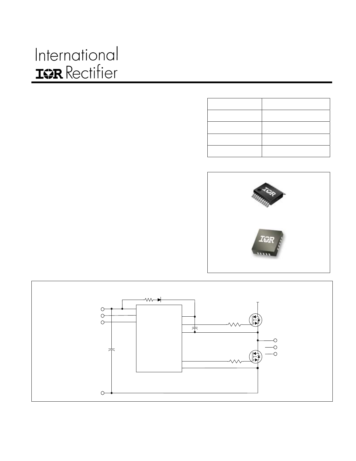
Typical Connection Diagram
HIN 1,2,3
LIN 1,2,3
HO 1,2,3
LO 1,2,3
Up to 600V
Vcc
LIN 1
,
2
,3
HIN 1
,
2
,3
TO
LOAD
V
B 1,2,3
V
S 1,2,3
Vcc
GND
COM
IRS2334
IRS2334SPbF/MPbF
www.irf.com
© 2010 International Rectifier
2
Table of Contents
Page
Description
3
Simplified Block Diagram
3
Typical Application Diagram
4
Qualification Information
5
Absolute Maximum Ratings
6
Recommended Operating Conditions
6
Static Electrical Characteristics
7
Dynamic Electrical Characteristics
7
Functional Block Diagram
8
Input/Output Pin Equivalent Circuit Diagram
9
Lead Definitions
10
Lead Assignments
11
Application Information and Additional Details
12
Parameter Temperature Trends
21
Package Details
25
Tape and Reel Details
27
Part Marking Information
29
Ordering Information
30
IRS2334SPbF/MPbF
www.irf.com
© 2010 International Rectifier
3
Description
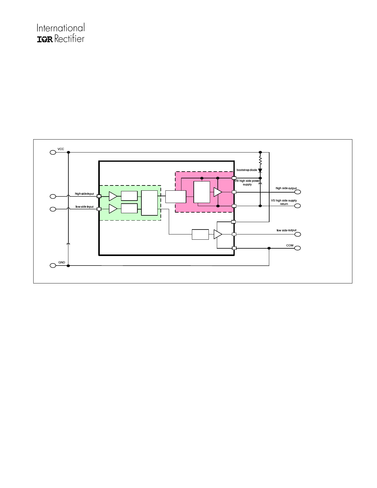
The IRS2334 is a high voltage, high speed power MOSFET and IGBT driver with three independent high side
and low side referenced output channels for 3-phase applications. Proprietary HVIC and latch immune CMOS
technology enables ruggedized monolithic construction. Logic inputs are compatible with CMOS or LSTTL
outputs, down to 3.3 V. The output drivers feature a high pulse current buffer stage designed for minimum
driver cross-conduction. Propagation delays are matched to simplify use in high frequency applications. The
floating channel can be used to drive N-channel power MOSFETs or IGBTs in the high side configuration up
to 600 V.
Simplified Block Diagram
to high side
power switches
(x3)
HV Level
Shifters
Delay
HV floating well
to low side
power switches
(x3)
Schmitt trigger, minimum dead time
and shoot-through protection
IRS2334SPbF/MPbF
www.irf.com
© 2010 International Rectifier
4
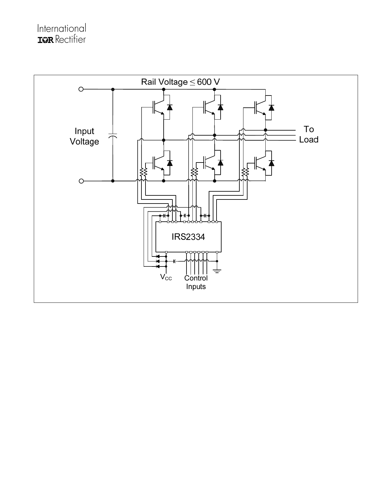
Typical Application Diagram
IRS2334SPbF/MPbF
www.irf.com
© 2010 International Rectifier
5
Qualification Information
†
Industrial
††
Qualification Level
Comments: This IC has passed JEDEC industrial
qualification. IR consumer qualification level is granted by
extension of the higher Industrial level.
Moisture Sensitivity Level
MSL2
, 260
C
(per IPC/JEDEC J-STD-020)
Human Body Model
Class 1C
(per JEDEC standard JESD22-A114)
ESD
Machine Model
Class B
(per EIA/JEDEC standard EIA/JESD22-A115)
IC Latch-Up Test
Class I, Level A
(per JESD78)
RoHS Compliant
Yes
†
Qualification standards can be found at International Rectifier’s web site
http://www.irf.com/
†† Higher qualification ratings may be available should the user have such requirements. Please contact your
International Rectifier sales representative for further information.
IRS2334SPbF/MPbF
www.irf.com
© 2010 International Rectifier
6
Absolute Maximum Ratings
Absolute maximum ratings indicate sustained limits beyond which damage to the device may occur. All voltage
parameters are absolute voltages referenced to COM unless otherwise specified. The thermal resistance and
power dissipation ratings are measured under board mounted and still air conditions.
Symbol Definition
Min.
Max.
Units
V
B
High side floating supply voltage
-0.3
625
V
S
High side floating supply offset voltage
V
B1,2,3
- 25
†
V
B1,2,3
+ 0.3
V
HO1,2,3
High side floating output voltage
V
S1,2,3
- 0.3
V
B1,2,3
+ 0.3
V
CC
Low side and logic fixed supply voltage
-0.3
25
†
V
LO1,2,3
Low side output voltage
-0.3
V
CC
+ 0.3
V
IN
Logic and analog input voltages
-0.3
V
CC
+ 0.3
V
PW
HIN
High-side input pulse width
500
—
ns
dV
S
/dt
Allowable offset supply voltage slew rate
—
50
V/ns
20 lead SOIC
— 1.14
P
D
Package power dissipation @ TA
≤ 25°C
28 lead MLPQ
—
3.363
W
20 lead SOIC
—
65.8
Rth
JA
Thermal resistance, junction to ambient
28 lead MLPQ
—
22.3
°C/W
T
J
Junction
temperature
— 150
T
S
Storage
temperature
-55 150
T
L
Lead temperature (soldering, 10 seconds)
—
300
°C
†
All supplies are fully tested at 25 V. An internal 25 V clamp exists for each supply.
Recommended Operating Conditions
For proper operation, the device should be used within the recommended conditions. All voltage parameters are
absolute voltages referenced to COM unless otherwise specified. The V
S1,2,3
offset ratings are tested with all
supplies biased at 15 V.
Symbol Definition
Min.
Max.
Units
V
B1,2,3
High side floating supply voltage
V
S1,2,3
+10 V
S1,2,3
+ 20
V
S1,2,3
Static high side floating supply offset voltage
†
-8 600
V
S1,2,3
(t)
Transient high side floating supply offset voltage
††
-50
600
V
HO1,2,3
High side floating output voltage
V
S1,2,3
V
B1,2,3
V
CC
Low side and logic fixed supply voltage
10
20
V
LO1,2,3
Low side output voltage
0
V
CC
V
IN
Logic input voltage
0
V
CC
V
T
A
Ambient temperature
-40 125
°C
† Logic operation for V
S
of –8 V to 600 V. Logic state held for V
S
of –8 V to –V
BS
.
†† Operational for transient negative V
S
of -50 V
with a 50 ns pulse width. Guaranteed by design. Refer to the
Application Information section of this datasheet for more details.
IRS2334SPbF/MPbF
www.irf.com
© 2010 International Rectifier
7
Static Electrical Characteristics
(V
CC
-COM) = (V
B1,2,3
-V
S1,2,3
) = 15 V and T
A
= 25
o
C unless otherwise specified. The V
IN
and I
IN
parameters are
referenced to COM. The V
O
and I
O
parameters are referenced to COM
and V
S1,2,3
and are applicable to the output
leads LO1,2,3 and HO1,2,3 respectively. The V
CCUV
and V
BSUV
parameters are referenced to COM
and V
S
respectively.
Symbol Definition Min.
Typ.
Max. Units Test
Conditions
V
IH
Logic “1” input voltage
2.5
—
—
V
IL
Logic “0” input voltage
—
—
0.8
V
IN
,
TH+
Input positive going threshold
—
1.9
—
V
IN
,
TH-
Input negative going threshold
—
1
—
V
OH
High level output voltage
—
0.9
1.4
V
OL
Low level output voltage
—
0.4
0.6
I
O
= 20 mA
V
CCUV+
V
BSUV+
V
CC
and V
BS
supply under-voltage positive
going threshold
10.4 11.1 11.6
V
CCUV-
V
BSUV-
V
CC
and V
BS
supply under-voltage negative
going threshold
10.2 10.9 11.4
V
CCUVH
V
BSUVH
V
CC
and V
BS
supply under-voltage hysteresis
0.1
0.2
—
V
I
LK
Offset supply leakage current
—
1
50
V
B
=V
S
= 600 V
I
QBS
Quiescent
V
BS
supply current
—
40
120
µA
I
QCC
Quiescent
V
CC
supply current
—
300
700
µA
V
IN
= 0 V
I
IN+
Logic “1” input bias current
—
150
250
V
IN
= 5 V
I
IN-
Logic “0” input bias current
—
1
µA
V
IN
= 0 V
I
o+
Output high short circuit pulsed current
120
200
—
I
o-
Output low short circuit pulsed current
250
350
—
mA
V
O
= 0 V or 15 V
PW ≤ 10 µs
Dynamic Electrical Characteristics
V
CC
= V
B1,2,3
= 15 V, V
S1,2,3
= COM, T
A
= 25
o
C and C
L
= 1000 pF unless otherwise specified.
Symbol Definition Min.
Typ.
Max. Units Test
Conditions
t
on
Turn-on propagation delay
400
530
750
t
off
Turn-off propagation delay
400
530
750
t
r
Turn-on rise time
—
125
190
t
f
Turn-off fall time
—
50
75
t
FILIN
Input filter time
200
350
510
V
IN
= 0V and 5V
DT Dead
time
190
290
420
MDT
Dead time matching
—
—
60
MT t
on
, t
off
propagation delay matching time
—
—
50
V
IN
= 0V & 5V
External dead time
0s
PM
PW pulse width distortion
†
— — 75
ns
PW input =10µs
†
PM is defined as PW
IN
- PW
OUT
.
IRS2334SPbF/MPbF
www.irf.com
© 2010 International Rectifier
8
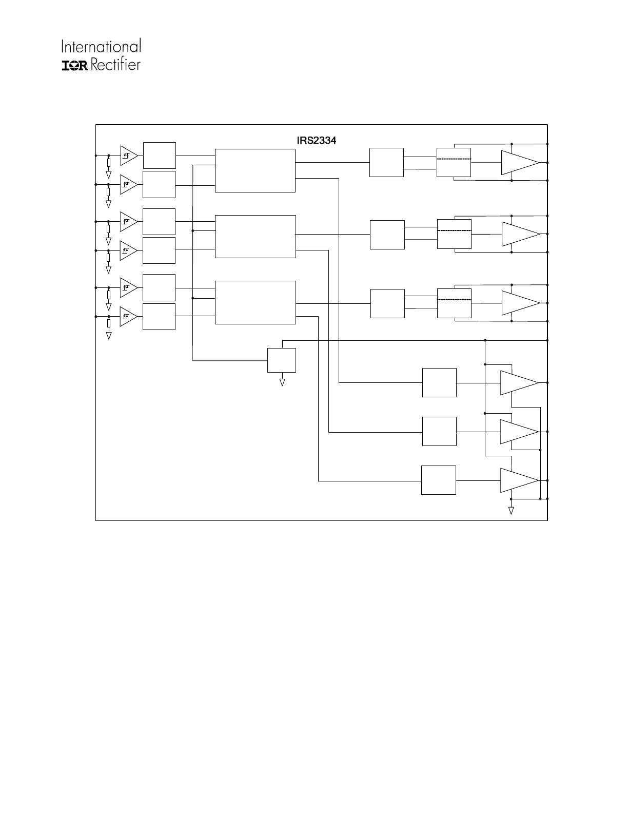
Functional Block Diagram
HIN1
RESET
SET
Deadtime &
Shoot-Through
Prevention
Deadtime &
Shoot-Through
Prevention
Deadtime &
Shoot-Through
Prevention
UV
Detect
Input
Noise
Filter
Input
Noise
Filter
Input
Noise
Filter
Input
Noise
Filter
Input
Noise
Filter
Input
Noise
Filter
HIN2
HIN3
LIN2
LIN1
LIN3
VB1
VS1
HO2
VB2
HO1
VS2
VB3
HO3
VS3
VCC
LO1
LO2
LO3
COM
HV
Level
Shifter
Delay
Delay
Delay
Latch
UV
Detect
Latch
UV
Detect
Latch
UV
Detect
RESET
SET
RESET
SET
Driver
Driver
Driver
Driver
Driver
Driver
HV
Level
Shifter
HV
Level
Shifter
SD
SD
SD
IRS2334SPbF/MPbF
www.irf.com
© 2010 International Rectifier
9
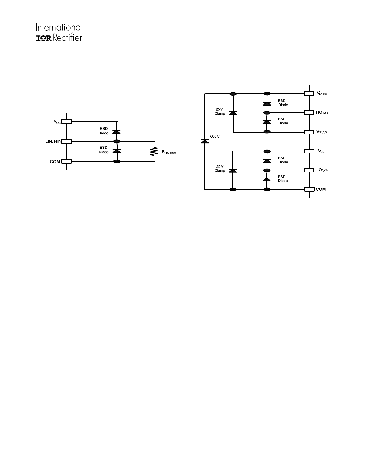
Input/Output Pin Equivalent Circuit Diagrams
IRS2334SPbF/MPbF
www.irf.com
© 2010 International Rectifier
10
Lead Definitions
Symbol Description
VCC
Low side and logic power supply
VB1
High side floating power supply (phase 1)
VB2
High side floating power supply (phase 2)
VB3
High side floating power supply (phase 3)
VS1
High side floating supply return (phase 1)
VS2
High side floating supply return (phase 2)
VS3
High side floating supply return (phase 3)
HIN1
Logic input for high side gate driver output HO1, input is in-phase with output
HIN2
Logic input for high side gate driver output HO2, input is in-phase with output
HIN3
Logic input for high side gate driver output HO3, input is in-phase with output
LIN1
Logic input for low side gate driver output LO1, input is in-phase with output
LIN2
Logic input for low side gate driver output LO2, input is in-phase with output
LIN3
Logic input for low side gate driver output LO3, input is in-phase with output
HO1
High side gate driver output (phase 1)
HO2
High side gate driver output (phase 2)
HO3
High side gate driver output (phase 3)
LO1
Low side gate driver output (phase 1)
LO2
Low side gate driver output (phase 2)
LO3
Low side gate driver output (phase 3)
COM
Low side supply return