
www.irf.com
© 2009 International Rectifier
1
September 30, 2009
Datasheet No – PD 97421
IRS2301S
HIGH AND LOW SIDE DRIVER
Features
• Floating channel designed for bootstrap operation
• Fully operational to +600V
• Tolerant to negative transient voltage – dV/dt immune
• Gate drive supply range from 5V to 20V
• Undervoltage lockout for both channels
• 3.3V, 5V and 15V input logic compatible
• Matched propagation delay for both channels
• Outputs in phase with inputs
• Lower di/dt gate driver for better noise immunity
• Leadfree, RoHS compliant
Typical Applications
o
Appliance motor drives
o
Servo
drives
o
Micro inverter drives
o
General purpose three phase inverters
Product Summary
V
OFFSET
600V
Max
V
OUT
5V – 20V
I
o+
& I
o-
(min)
120mA / 250mA
t
ON
& t
OFF
(typical)
220ns / 200ns
Delay Matching
50ns
Package Options
8-Lead SOIC
IRS2301S
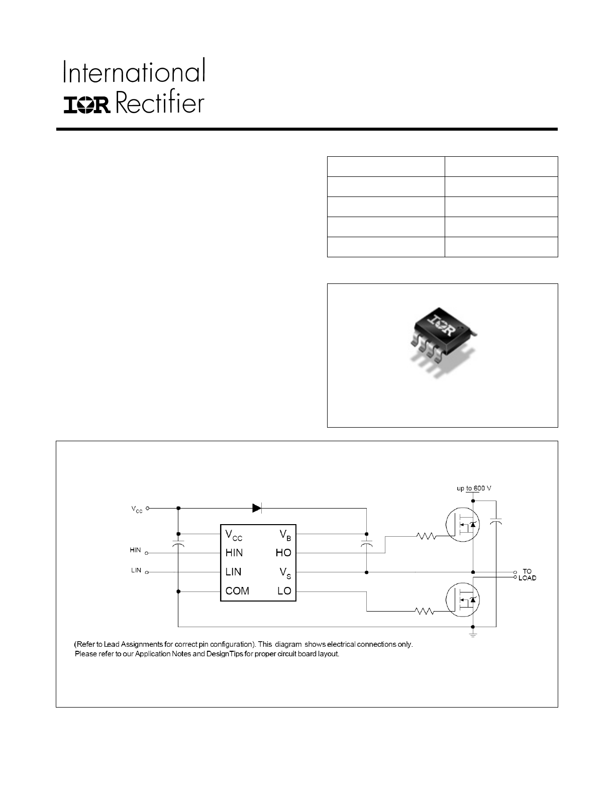
Typical Connection Diagram
IRS2301S
www.irf.com
© 2009 International Rectifier
2
Table of Contents
Page
Typical Connection Diagram
1
Description
3
Feature Comparison
3
Qualification Information
4
Absolute Maximum Ratings
5
Recommended Operating Conditions
5
Dynamic Electrical Characteristics
6
Static Electrical Characteristics
6
Functional Block Diagram
7
Input/output Timing Diagram
8
Lead Definitions
9
Lead Assignments
9
Application Information and Additional Details
10
Package Details
11
Tape and Reel Details
12
Part Marking Information
13
Ordering Information
14

IRS2301S
www.irf.com
© 2009 International Rectifier
3
Description
The IRS2301S is a high voltage, high speed power MOSFET and IGBT driver with independent high- and low-
side referenced output channels. Proprietary HVIC and latch immune CMOS technologies enable ruggedized
monolithic construction. The logic input is compatible with standard CMOS or LSTTL output, down to 3.3V logic.
The output drivers feature a high pulse current buffer stage. The floating channel can be used to drive an N-
channel power MOSFET or IGBT in the high-side configuration which operates up to 600V.
IRS2301S
www.irf.com
© 2009 International Rectifier
4
Qualification Information
†
Industrial
††
Qualification Level
Comments: This family of ICs has passed JEDEC’s
Industrial qualification. IR’s Consumer qualification level
is granted by extension of the higher Industrial level.
Moisture Sensitivity Level
MSL2
†††
260°C
(per IPC/JEDEC J-STD-020)
Machine Model
Class B
(per JEDEC standard JESD22-A115)
ESD
Human Body Model
Class 2
(per EIA/JEDEC standard EIA/JESD22-A114)
IC Latch-Up Test
Class I, Level A
(per JESD78)
RoHS Compliant
Yes
†
Qualification standards can be found at International Rectifier’s web site
http://www.irf.com/
††
Higher qualification ratings may be available should the user have such requirements. Please contact
your International Rectifier sales representative for further information.
††† Higher MSL ratings may be available for the specific package types listed here. Please contact your
International Rectifier sales representative for further information.
IRS2301S
www.irf.com
© 2009 International Rectifier
5
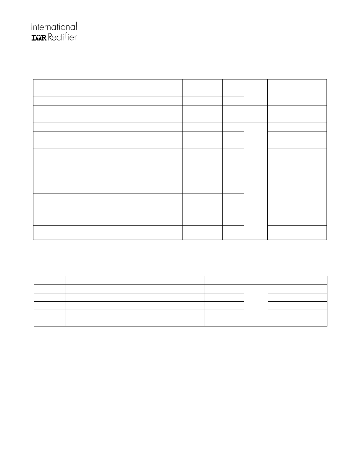
Absolute Maximum Ratings
Absolute Maximum Ratings indicate sustained limits beyond which damage to the device may occur. All voltage
parameters are absolute voltages referenced to COM. The thermal resistance and power dissipation ratings are
measured under board mounted and still air conditions.
Recommended Operating Conditions
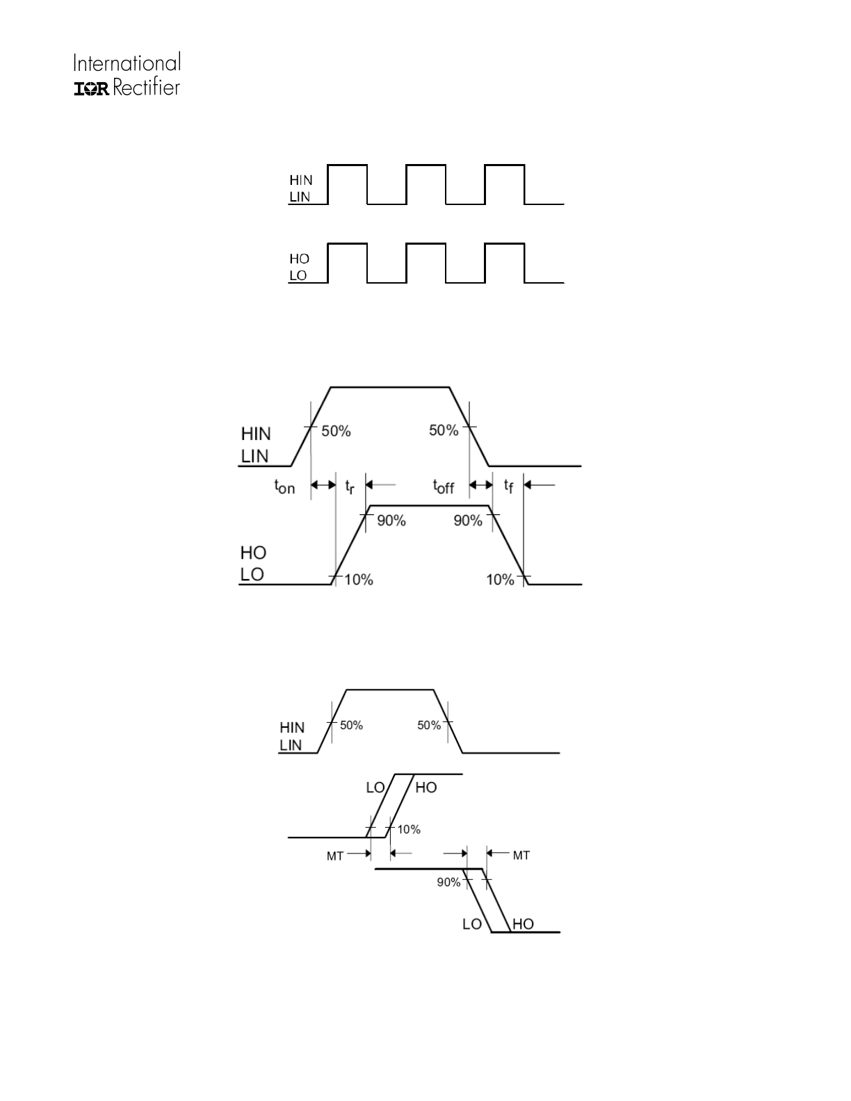
The input/output logic timing diagram is shown in Fig. 1. For proper operation the device should be used within
the recommended conditions. The V
S
offset rating is tested with all supplies biased at 15V differential.
†: Logic operational for V
S
of -5 V to +600 V. Logic state held for V
S
of -5 V to – V
BS.
(Please refer to the Design Tip DT97 -3 for more details).
Symbol Definition
Min.
Max.
Units
V
B
High-side floating absolute voltage
-0.3
625
V
S
High-side floating supply offset voltage
V
B
- 25
V
B
+ 0.3
V
HO
High-side floating output voltage
V
S
- 0.3
V
B
+ 0.3
V
CC
Low-side and logic fixed supply voltage
-0.3
25
V
LO
Low-side output voltage
-0.3
V
CC
+ 0.3
V
IN
Logic input voltage (HIN & LIN)
COM -0.3 V
CC
+ 0.3
V
dV
S
/dt
Allowable offset supply voltage transient
—
50
V/ns
P
D
Package power dissipation @ TA ≤ 25°C
—
0.625
W
Rth
JA
Thermal resistance, junction to ambient
—
200
°C/W
T
J
Junction temperature
— 150
T
S
Storage temperature
-50 150
T
L
Lead temperature (soldering, 10 seconds)
— 300
°C
Symbol Definition
Min.
Max.
Units
V
B
High-side floating supply absolute voltage
V
S
+ 5
V
S
+ 20
V
S
High-side floating supply offset voltage
† 1
600
V
HO
High-side floating output voltage
V
S
V
B
V
CC
Low-side and logic fixed supply voltage
5
20
V
LO
Low-side output voltage
0
V
CC
V
IN
Logic input voltage (HIN & LIN)
COM
V
CC
V
T
A
Ambient temperature
-40
125
°C
IRS2301S
www.irf.com
© 2009 International Rectifier
6
Static Electrical Characteristics
V
BIAS
(V
CC
, V
BS
) = 15V and T
A
= 25°C unless otherwise specified. The V
IL,
V
IH
and I
IN
parameters are
referenced to COM and are applicable to the respective input leads: HIN and LIN. The V
O,
I
O
and R
on
parameters are referenced to COM and are applicable to the respective output leads: HO and LO.
Dynamic Electrical Characteristics
V
BIAS
(V
CC
, V
BS
) = 15V, C
L
= 1000pF, T
A
= 25°C unless otherwise specified.
Symbol Definition Min
Typ
Max
Units
Test
conditions
V
IH
Logic “1” input voltage
2.5
—
—
V
IL
Logic “0” input voltage
—
—
0.8
V V
CC
= 10V to 20V
V
OH
High level output voltage, V
BIAS
-
V
O
—
—
0.2
V
OL
Low level output voltage, V
O
—
—
0.1
V I
O
= 2mA
I
LK
Offset supply leakage current
—
—
50
V
B
=
V
S
= 600V
I
QBS
Quiescent
V
BS
supply current
60
160
260
I
QCC
Quiescent
V
CC
supply current
60
160
260
V
IN
= 0V or 5V
I
IN+
Logic “1” input bias current
—
5
20
V
IN
= 5V
I
IN-
Logic “0” input bias current
—
—
5
µA
V
IN
= 0V
V
CCUV+
V
BSUV+
V
CC
and V
BS
supply undervoltage positive
going threshold
3.3 4.1 5
V
CCUV-
V
BSUV-
V
CC
and V
BS
supply undervoltage negative
going threshold
3 3.8 4.7
V
CCUVH
V
BSUVH
Hysteresis 0.1
0.3
—
V
I
O+
Output high short circuit pulsed current
—
200
—
V
O
= 0V,
PW ≤ 10µs
I
O-
Output low short circuit pulsed current
—
350
—
mA
V
O
= 15V,
PW ≤ 10µs
Symbol Definition Min
Typ
Max
Units
Test
conditions
t
on
Turn-on propagation delay
—
220
300
V
S
= 0V
t
off
Turn-off propagation delay
—
200
280
V
S
= 0V or 600V
MT
Delay matching, HS & LS turn-on/off
—
0
50
t
r
Turn-on rise time
—
130
220
t
f
Turn-off fall time
—
50
80
ns
V
S
= 0V
IRS2301S
www.irf.com
© 2009 International Rectifier
7
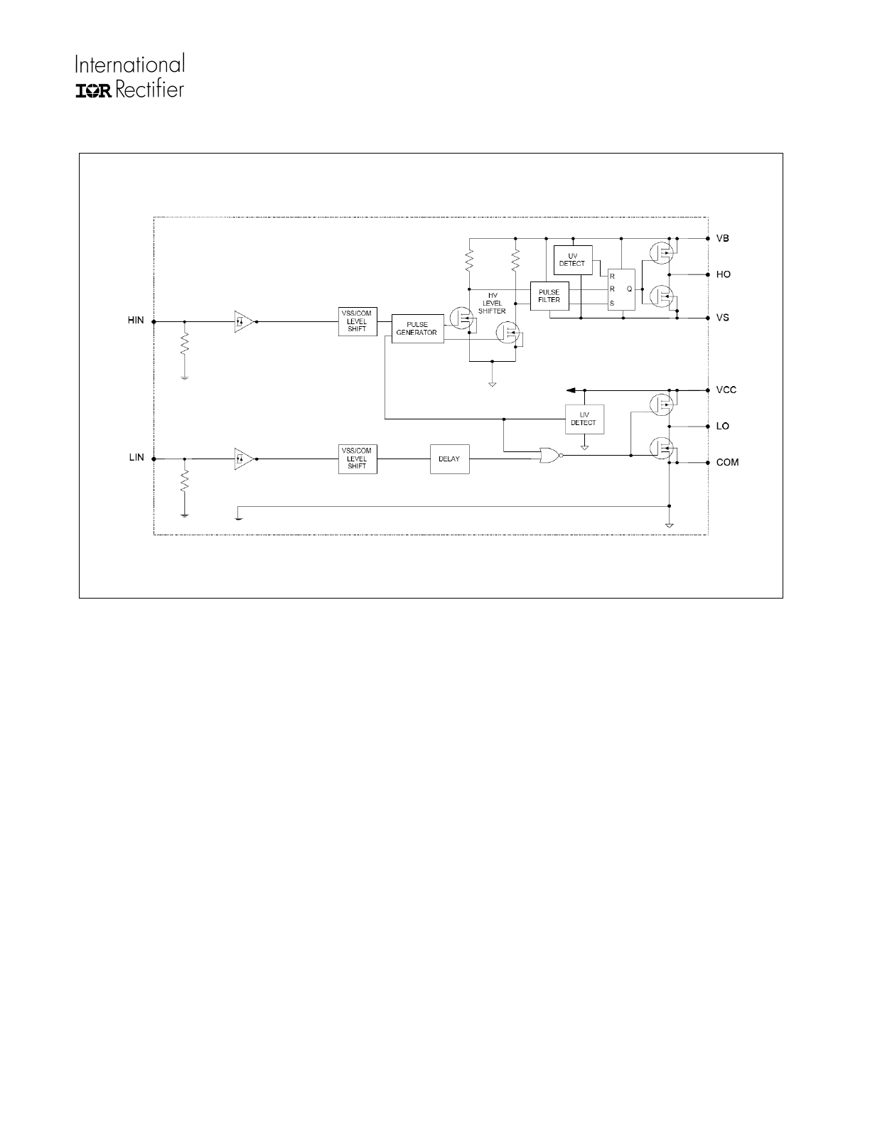
Functional Block Diagram:
IRS2301S
www.irf.com
© 2009 International Rectifier
8
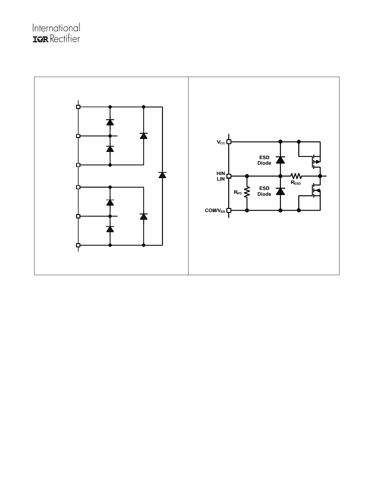
Input/Output Pin Equivalent Circuit
Diagrams:
V
CC
COM/V
SS
LO
ESD
Diode
ESD
Diode
V
B
V
S
HO
ESD
Diode
ESD
Diode
25V
25V
600V
IRS2301S
www.irf.com
© 2009 International Rectifier
9
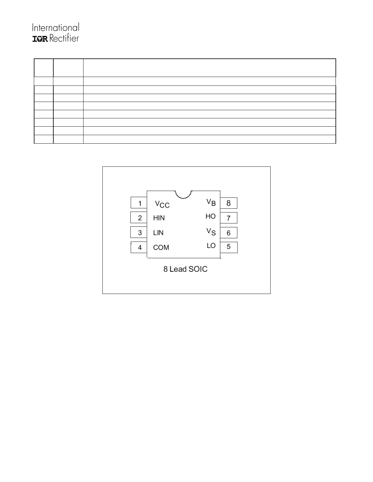
Lead Definitions:
PIN# Symbol
Description
1
V
CC
Low-side and logic fixed supply
2
HIN
Logic input for high-side gate driver outputs (HO), in phase with HO
3
LIN
Logic input for low-side gate driver outputs (LO), in phase with LO
4
COM Low-side
return
5
LO
Low-side gate drive output
6
V
S
High-side floating supply return
7
HO
High-side gate drive output
8 V
B
High-side floating supply
Lead Assignments
IRS2301S
www.irf.com
© 2009 International Rectifier
10
Application Information and Additional Details
Figure 1: Input/Output Timing Diagram
Figure 2: Switching Time Waveform Definitions
Figure 3: Delay Matching Waveform Definitions