
www.irf.com
© 2007 International Rectifier
Datasheet No – PD97383
March 17, 2009
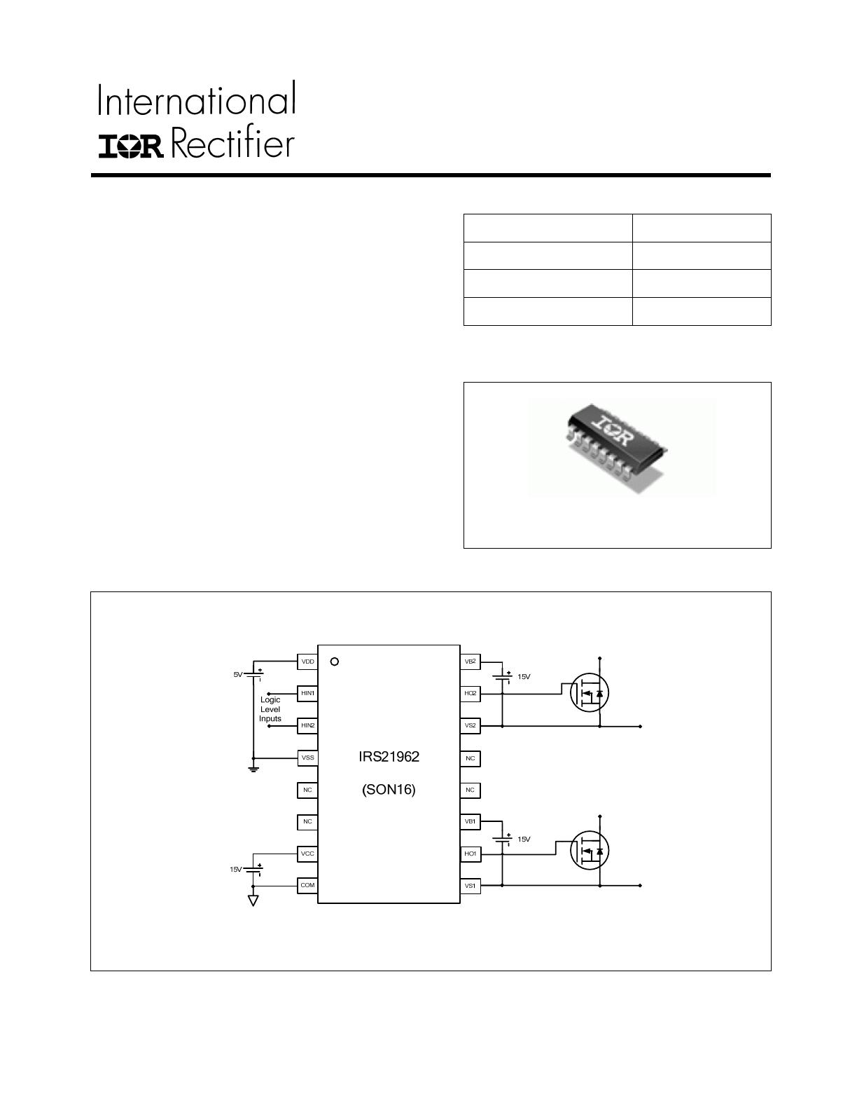
IRS21962S
Dual channel high-side drivers with floating input
Features
•
Two independent high side output channels
•
CMOS Schmitt trigger inputs with pull down resistor
•
5V compatible logic level inputs
•
Immune to –Vs spike and tolerant to dVs/dt and
dVss/dt
•
Typical operating frequency 200kHz
• RoHS
compliant
Product Summary
V
OFFSET
600
V
V
OUT
10 V – 20 V
I
o+
& I
o-
(typical)
0.5 A
t
ON
& t
OFF
(typical)
90 ns
Package Type
16-Lead SOIC (narrow body)
Typical Connection Diagram
IRS21962S
www.irf.com
© 2008 International Rectifier
2
Table of Contents
Page
Description
3
Qualification Information
4
Absolute Maximum Ratings
5
Recommended Operating Conditions
5
Static Electrical Characteristics
6
Dynamic Electrical Characteristics
6
Functional Block Diagram
7
Input/Output Pin Equivalent Circuit Diagram
9
Lead Definitions
10
Lead Assignments
10
Package Details
11
Tape and Reel Details
12
Part Marking Information
13
Ordering Information
14

IRS21962S
www.irf.com
© 2008 International Rectifier
3
Description
The IRS21962 is a high voltage, high speed power MOSFET and IGBT driver with propagation delay matched
output channels. Proprietary HVIC and latch immune CMOS technologies enable ruggedized monolithic
construction. The floating logic input is compatible with standard 5 V CMOS or LSTTL logic and can be
operated up to 600 volts above the COM ground. The output driver feature a 500 mA high pulse current buffer
stage designed for minimum driver cross-conduction. The floating channel can be used to drive an N-channel
power MOSFET or IGBT in the high side configuration, which operates up to 600 V above COM ground.
IRS21962S
www.irf.com
© 2008 International Rectifier
4
Qualification Information
†
Industrial
††
Qualification Level
Comments: This family of ICs has passed JEDEC’s
Industrial qualification. IR’s Consumer qualification
level is granted by extension of the higher Industrial
level.
Moisture Sensitivity Level
SOIC16N
MSL2
†††
260°C
(per IPC/JEDEC J-STD-020)
Machine Model
Class B
(per JEDEC standard JESD22-A115)
ESD
Human Body Model
Class 2
(per EIA/JEDEC standard EIA/JESD22-A114)
IC Latch-Up Test
Class 1, Level A
(per JESD78)
RoHS Compliant
Yes
†
Qualification standards can be found at International Rectifier’s web site
http://www.irf.com/
††
Higher qualification ratings may be available should the user have such requirements. Please contact
your International Rectifier sales representative for further information.
†††
Higher MSL ratings may be available for the specific package types listed here. Please contact your
International Rectifier sales representative for further information.
IRS21962S
www.irf.com
© 2008 International Rectifier
5
Absolute Maximum Ratings
Absolute maximum ratings indicate sustained limits beyond which damage to the device may occur. All
voltage parameters are absolute voltages referenced to COM, which is the –200V DC bus provided
externally.
Symbol Definition Min
Max
Units
VCC
Low side supply voltage
-0.3
25
V
VDD
Input logic supply voltage
-0.3
625
V
VSS
Input logic supply return
VDD-25
VDD+0.3
V
HIN1, HIN2
Input logic voltage
VSS-0.3
VDD+0.3
V
VB1, VB2
High side floating well positive supply voltage
-0.3
625
V
VS1
High side floating well negative supply voltage
VB1-25
VB1+0.3
V
VS2
High side floating well negative supply voltage
VB2-25
VB2+0.3
V
HO1
Floating gate drive output voltage
VS1-0.3
VB1+0.3
V
HO2
Floating gate drive output voltage
VS2-0.3
VB2+0.3
V
dVS/dt
Allowable VS1 or VS2 offset supply transient relative to
COM
- 50
V/ns
dVSS/dt
Allowable VSS input supply transient relative to COM
-
50
V/ns
P
D
Package Power Dissipation @ T
A
<=+25°C
- 1
W
R
θJA
Thermal Resistance, Junction to Ambient
-
100
°C/W
T
J
Junction Temperature
-55
150
°C
T
S
Storage Temperature
-55
150
°C
T
L
Lead temperature (Soldering, 10 seconds)
-
300
°C
Recommended Operating Conditions
For proper operation, the device should be used within the recommended conditions. All voltage parameters
are absolute voltages referenced to COM, which is the –200V DC bus provided externally. The offset rating
are tested with supplies of (VDD-VSS)=5V and (VCC-COM)=(VB1-VS1)= (VB2-VS2)=15V.
Symbol Definition Min
Max
Units
VCC
Low side supply voltage
10
20
V
VDD
Input logic supply voltage
VSS+4.5
VSS+5.5
V
VSS
Input logic supply offset voltage
-0.3
600
V
HIN1, HIN2
IN1~IN2 input voltage
VSS
VDD
V
VB1
High side floating well positive supply voltage
VS1+10
VS1+20
V
VB2
High side floating well positive supply voltage
VS2+10
VS2+20
V
VS1, VS2
High side floating well negative supply voltage
-5
600
V
HO1
Floating gate drive output voltage
VS1
VB1
V
HO2
Floating gate drive output voltage
VS2
VB2
V
T
A
Ambient Temperature
-40
125
°C
IRS21962S
www.irf.com
© 2008 International Rectifier
6
Static Electrical Characteristics
(VDD-VSS)=5V and (VCC-COM)=(VBn-VSn)=15V. TA = 25°C. The parameters VIN,th+, VIN,th-, IIN+, IIN-
, VDDUV+, and VDDUV- are referenced to VSS. The VBSUV+, VBSUV-, VOH, VOL, IO+, and IO-
parameters are referenced to VS1 or VS2. The VCCUV+, VCCUV- parameters are referenced to COM.
Symbol Definition
Min
Typ
Max
Units
Test
Conditions
V
DDUV+
V
DD
supply undervoltage positive going threshold
4.0 V
V
SS
-COM = 5V
V
DDUV-
V
DD
supply undervoltage negative going threshold
3.9 V
V
SS
-COM = 5V
V
DDUVH
V
DD
supply undervoltage lockout hysteresis
0.1 V
V
SS
-COM = 5V
V
CCUV+
V
CC
supply undervoltage positive going threshold
7.5 8.6 9.7 V
V
CCUV-
V
CC
supply undervoltage negative going threshold
7.1 8.2 9.3 V
V
CCUVH
V
CC
supply undervoltage lockout hysteresis
--- 0.4 --- V
V
BSUV+
V
BS
supply undervoltage positive going threshold
7.5 8.3 9.4 V
V
BSUV-
V
BS
supply undervoltage negative going threshold
6.9 7.7 8.8 V
V
BSUVH
V
BS
supply undervoltage lockout hysteresis
--- 0.6 --- V
I
LKDD
Input Logic offset supply leakage current
---
---
50
V
DD
= V
SS
= 600V
I
LKBS
Highside floating well offset supply leakage current
---
---
50
µA
V
B
= V
S
= 600V
I
QDD
Quiescent VDD supply current
---
105
180
V
IN
= 0V or 5V
I
QBS
Quiescent VBS supply current
---
100
175
V
IN
= 0V or 5V
I
QCC
Quiescent VCC supply current
---
180
280
uA
V
IN
= 0V or 5V
V
IN,th+
Logic “1” input threshold
3.5
V
IN,th-
Logic “0” input threshold
0.6 V
V
OH
High level output voltage, V
O
-V
BIAS
---
---
1
Io+=20mA
V
OL
Low level output voltage, V
O
---
---
1
V
Io-=20mA
I
IN+
Logic “1” input bias current
---
5
---
V
IN
=5V
I
IN-
Logic “0” input bias current
---
0
---
uA
V
IN
=0V
I
O+
Output high short circuit pulsed current
---
500
---
mA
VO=15V,
V
IN
=5V
,
PW<=10us
I
O
-
Output low short circuit pulsed current
---
500
---
mA
V
O
=0V,V
IN
=0VP,
W<=10us
Dynamic Electrical Characteristics
(VDD-VSS)=5V and (VCC-COM)=(VBn-VSn)=15V. TA = 25. °C C
L
= 1000pF unless otherwise specified.
All parameters are reference to COM.
Symbol Definition
Min
Typ
Max
Unit Test
Conditions
t
on
, t
off
Propagation delay from input pin HIN to output
pin HO
55 90 125
ns
Vss=200V, Vs=0V
t
r
Turn-on 10%-to-90% rise time at HO pin
25
70
ns
Vss=200V, Vs=0V
t
f
Turn-off 90%-to-10% fall time at HO pin
25
70
ns
Vss=200V, Vs=0V
IRS21962S
www.irf.com
© 2008 International Rectifier
7
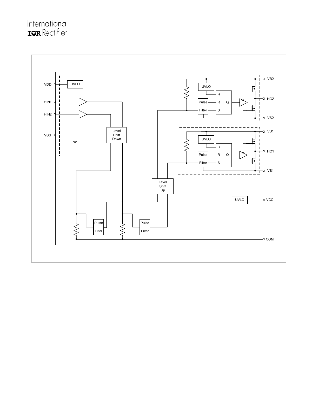
Figure 1 Functional Block Diagram
IRS21962S
www.irf.com
© 2008 International Rectifier
8
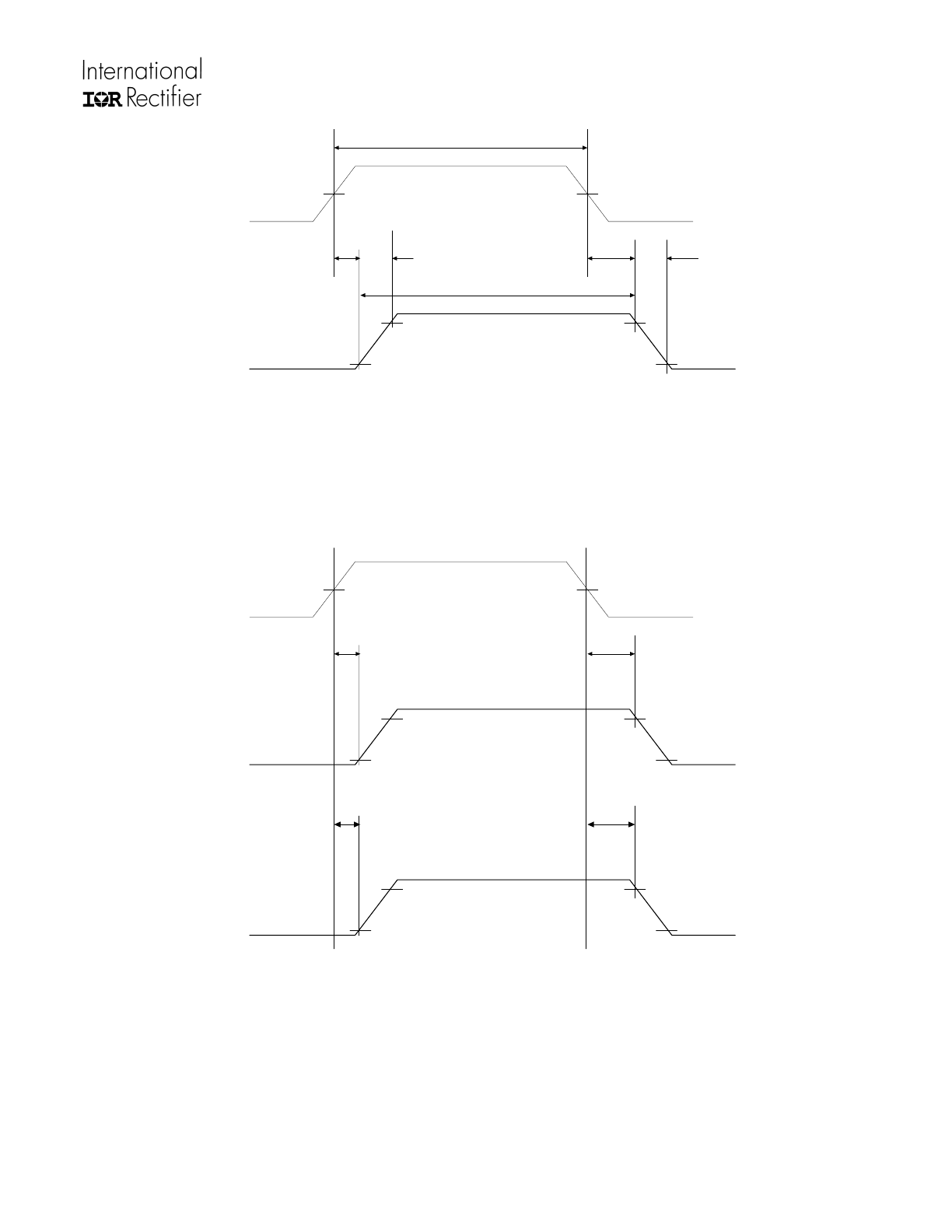
Input H IN
Output H O
t
on
t
r
50%
90%
10%
50%
90%
10%
t
off
t
f
PW
in
PW
out
Figure 2 Switching Time Waveforms
HIN1 and HIN2 of
Part A and Part B
HO1 or HO 2
of Part A
t
onA
50%
90%
10%
50%
90%
10%
t
offA
t
f
HO1 or HO 2
of Part B
t
onB
90%
10%
90%
10%
t
offB
Figure 3 Switching Time Waveforms – Part to Part Propagation Delay Matching
IRS21962S
www.irf.com
© 2008 International Rectifier
9
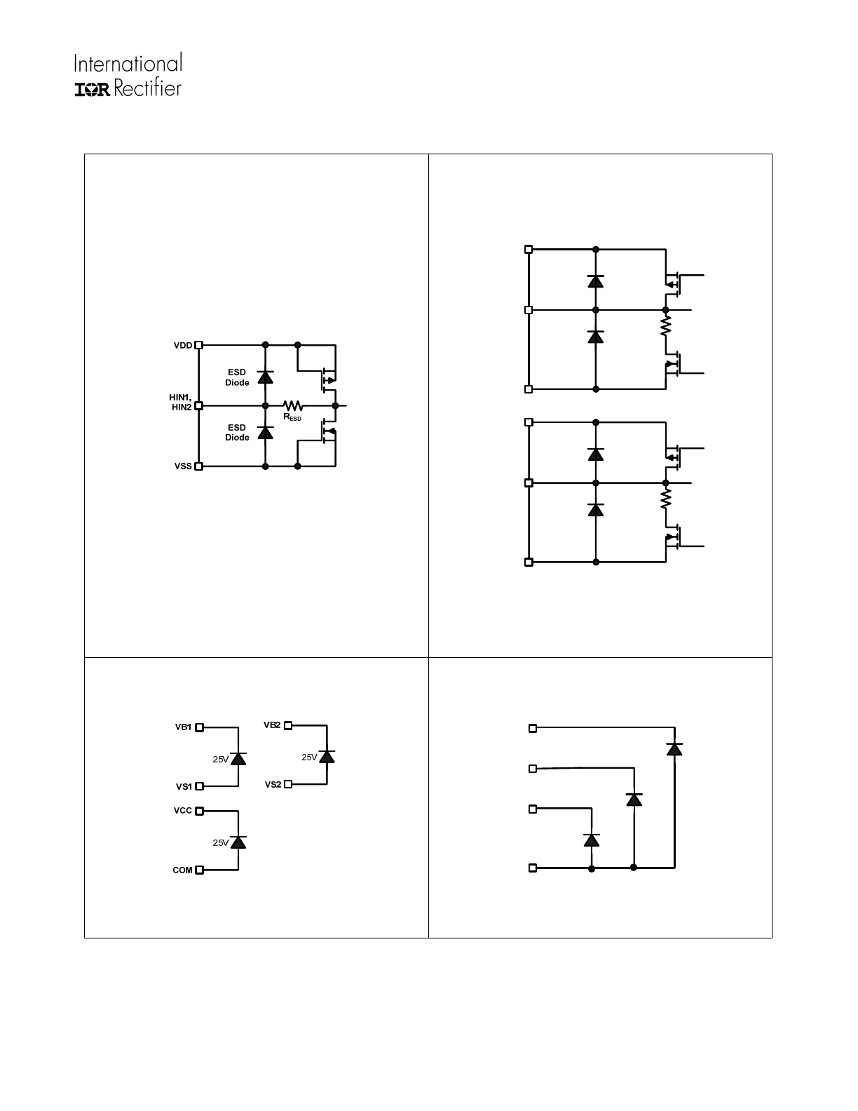
Input/Output Pin Equivalent Circuit
Diagrams
VB1
VS1
HO1
ESD
Diode
ESD
Diode
R
ESD
VB2
VS2
HO2
ESD
Diode
ESD
Diode
R
ESD
VB1
COM
VB2
VDD
600V
600V
600V
IRS21962S
www.irf.com
© 2008 International Rectifier
10
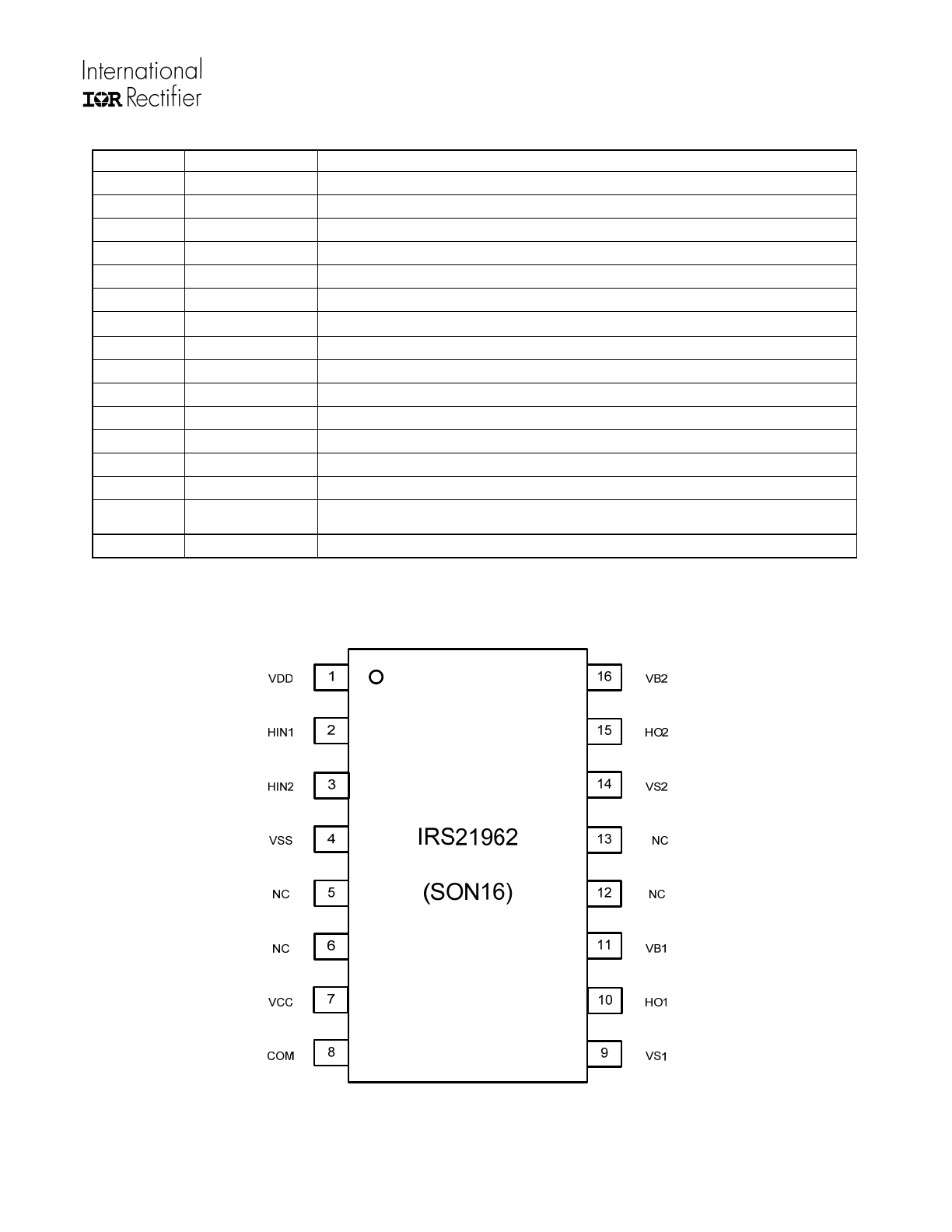
Lead Definitions:
Pin Symbol
Description
1 VDD
Input logic supply voltage
2 HIN1
Logic input channel 1
3
HIN2
Logic input channel 2
4
VSS
Input logic offset voltage
5 NC
No
connection
6 NC
No
connection
7
VCC
Low side supply voltage
8 COM
Ground
9
VS1
High side floating well offset voltage
10
HO1
Floating gate driver output voltage channel 1
11
VB1
High side floating well positive supply
12 NC
No
connection
13 NC
No
connection
14
VS2
High side floating well offset voltage
15
HO2
Floating gate driver output voltage channel 2
16
VB2
High side floating well positive supply
Lead Assignments