
www.irf.com Page 1
Data Sheet No. PD60310
IRS2168D(S)PbF
ADVANCED PFC + BALLAST CONTROL IC
Features
PFC, ballast control and 600 V half-bridge driver in one IC
Critical-conduction mode boost-type PFC
Programmable PFC over-current protection
Programmable half-bridge over-current protection
Programmable preheat frequency
Programmable preheat time
Programmable ignition ramp
Programmable run frequency
Closed-loop ignition current regulation
RoHs compliant
Description
The IRS2168D is a fully integrated, fully protected 600 V
ballast control IC designed to drive all types of fluorescent
lamps. The IRS2168D is based on the popular IR2166
control IC with additional improvements to increase ballast
performance. The PFC circuitry operates in critical
conduction mode and provides high PF, low THD and DC
bus regulation. The IRS2168D features include
programmable preheat and run frequencies, programmable
preheat time, programmable PFC over-current protection,
closed-loop half-bridge ignition current regulation, and
programmable end-of-life protection. Comprehensive
protection features such as protection from failure of a lamp
to strike, filament failures, end-of-life protection, DC bus
undervoltage reset as well as an automatic restart function,
have been included in the design.
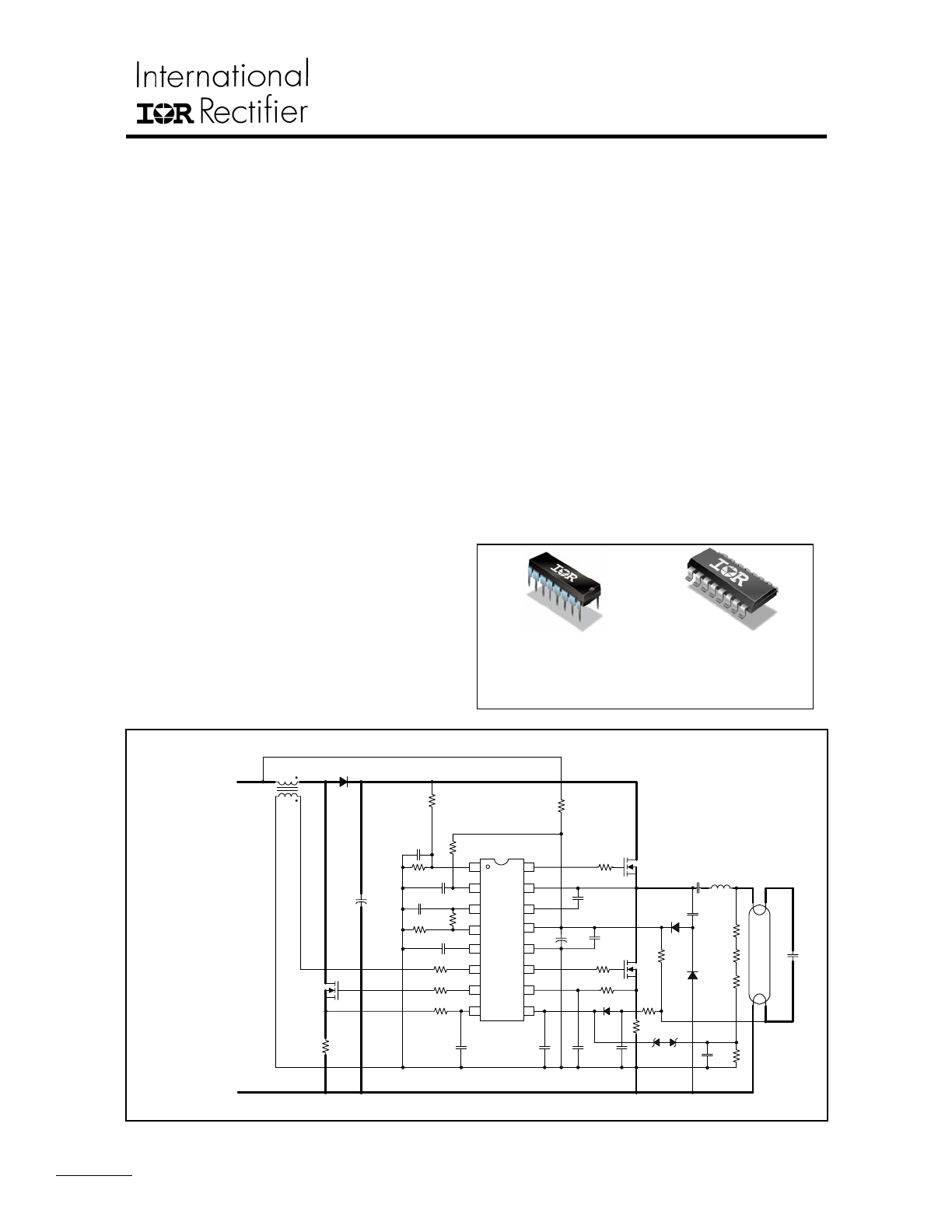
Application Diagram (Typical Only)
Fixed internal 1.6 µs HO and LO deadtime
Voltage-controlled oscillator (VCO)
End-of-life window comparator pin
Internal 65-event current sense up/down fault counter
DC bus undervoltage reset
Lamp removal/auto-restart shutdown pin
Internal bootstrap MOSFET
Internal 15.6 V Zener clamp diode on V
cc
Micropower startup (250 µA)
Latch immunity and ESD protection
System Features
One-chip ballast control solution
Wide range PFC for universal input and multi-lamp ballasts
Ultra low THD
Closed-loop ignition regulation for reliable lamp ignition
End-of-Life window comparator with internal OTA
Lamp removal/auto-restart function
Fault counter for robust noise immunity
Brown-out protection and reset
Internal bootstrap MOSFET
Packages
16-Lead PDIP 16-Lead SOIC
IRS2168DPbF IRS2168DSPbF
+ Rectified AC Line
- Rectified AC Line
R
VBUS1
15
14
13
12
11
IRS21
68D
COM
VCC
VB
VS
HO
1
2
3
CPH
PFC
VBUS
4
5
7
OC
FMIN
VCO
6
7
8
ZX
COMP
10
CS
LO
9
SD/EOL
16
D
BUS
D
CP2
M3
+
C
VBUS
R
VBUS
C
VCO
C
PH
C
COMP
C
BUS
R
GHS
M1
R
GPFC
L
RES
C
BLOCK
C
CS
R
CS
R
GLS
M2
R
5
R
4
R
SUPPLY
C
BOOT
C
SNUB
D
CP1
R
3
C
VCC2
C
VCC1
+
C
RES
C
SD1
C
SD2
R
6
R
7
R
8
R
9
D
1
D
2
D
3
R
1
C
EOL
R
OC
R
2
C
OC
R
FMIN
R
CPH
R
RPH
* Please note that this datasheet contains advanced information that could change before the product is released to production.
IRS2168D(S)PbF
www.irf.com Page 2
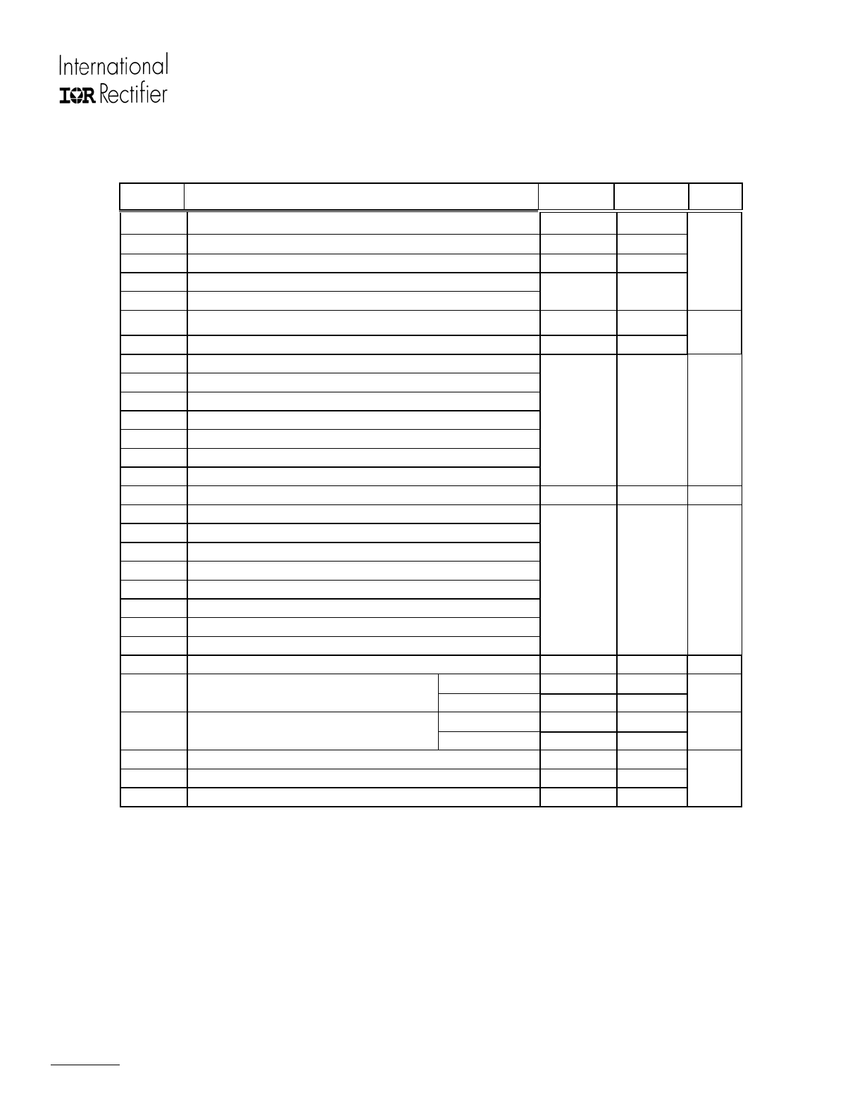
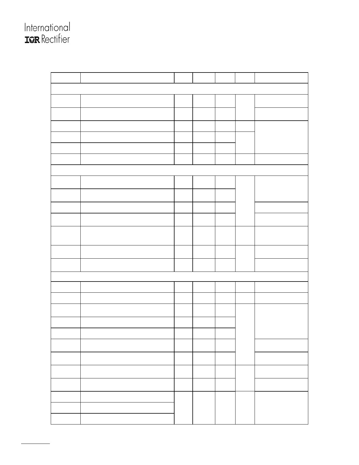
Absolute Maximum Ratings
Absolute maximum ratings indicate sustained limits beyond which damage to the device may occur. All voltage
parameters are absolute voltages referenced to COM, all currents are defned positive into any lead. The thermal
resistance and power dissipation ratings are measured under board mounted and still air conditions.
Symbol Definition
Min.
Max.
Units
V
B
V
B
pin high-side floating supply voltage
-0.3
625
V
S
V
S
pin high-side floating supply offset voltage
V
B
– 25
V
B
+ 0.3
V
HO
HO pin high-side floating output voltage
V
S
- 0.3
V
B
+ 0.3
V
LO
LO pin low-side output voltage
V
PFC
PFC gate driver output voltage
-0.3 V
CC
+ 0.3
V
I
O,MAX
Maximum allowable output current (HO, LO, PFC) due to external
power transistor miller effect
-500 500
I
CC
V
CC
current (see Note 1)
-25
25
mA
V
BUS
VBUS pin voltage
V
CPH
CPH pin voltage
V
COMP
COMP pin voltage
V
ZX
ZX pin voltage
V
OC
OC pin voltage
V
SD/EOL
SD/EOL pin voltage
V
CS
CS pin voltage
-0.3 V
CC
+ 0.3
V
V
VCO
VCO pin voltage
-0.3
6
V
I
CPH
CPH pin current
I
VCO
VCO pin current
I
FMIN
FMIN pin current
I
COMP
COMP pin current
I
ZX
ZX pin current
I
OC
OC pin current
I
SD/EOL
SD/EOL pin current
I
CS
CS pin current
-5 5
mA
dV/dt Allowable
V
S
pin offset voltage slew rate
-50
50
V/ns
Package power dissipation @ T
A
≤ +25 ºC
(16-Pin DIP)
--- 1.8
P
D
PD = (T
JMAX-
T
A
)/R
θJA
(16-Pin SOIC)
---
1.4
W
(16-Pin DIP)
---
70
R
θJA
Thermal resistance, junction to ambient
(16-Pin SOIC)
---
86
ºC/W
T
J
Junction temperature
-55
150
T
S
Storage temperature
-55
150
T
L
Lead temperature (soldering, 10 seconds)
---
300
ºC
Note 1: This IC contains a Zener clamp structure between the chip V
CC
and COM which has a nominal breakdown
voltage of 15.6 V. This supply pin should not be driven by a DC, low impedance power source greater than the V
CLAMP
specified in the Electrical Characteristics section.
IRS2168D(S)PbF
www.irf.com Page 3
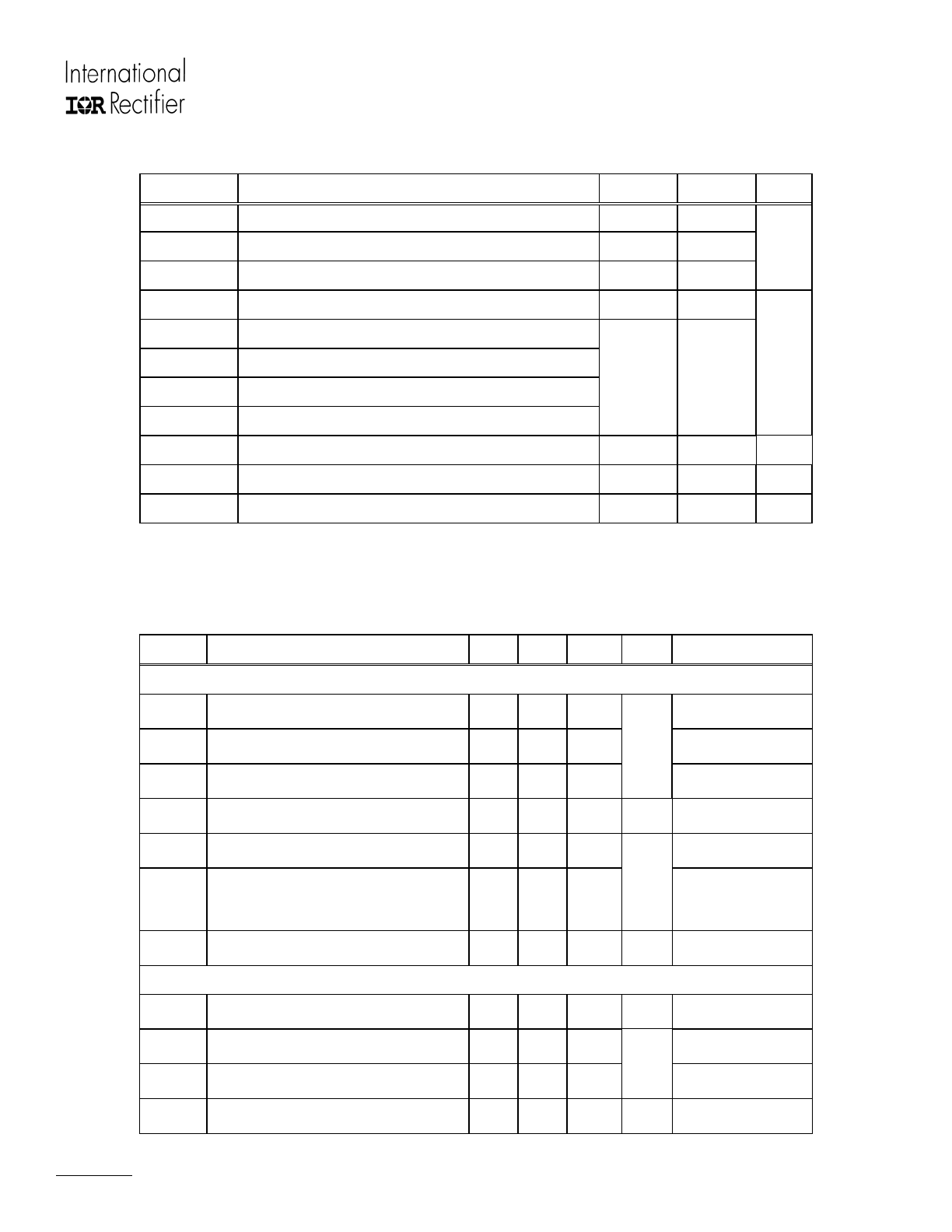
Recommended Operating Conditions
For proper operation the device should be used within the recommended conditions.
Symbol Definition Min.
Max.
Units
V
B
-V
S
High-side floating supply voltage
V
BSUV+
V
CLAMP
V
S
Steady state high-side floating supply offset voltage
-1
600
V
CC
Supply voltage
V
CCUV+
V
CLAMP
V
I
CC
V
CC
supply current
Note 2
10
I
SD/EOL
SD/EOL pin current
I
CS
CS pin current
I
OC
OC pin current
I
ZX
ZX pin current
-1 1
mA
V
VCO
VCO pin voltage
0
5
V
R
FMIN
FMIN pin programming resistor
10
300
k
Ω
T
J
Junction temperature
-25
125
ºC
Note 2: Enough current should be supplied into the V
CC
pin to keep the internal 15.6 V Zener clamp diode on this pin
regulated at its voltage, V
CLAMP
.
Electrical Characteristics
V
CC
= V
BS
= V
BIAS
=14 V +/- 0.25 V, C
LO
= C
HO
= C
PFC
= 1000 pF, R
FMIN
= 42.2 k
Ω, R
PH
= N/C, V
CPH
= V
VCO
= 0 V,
V
SD/EOL
= V
COMP
= V
CS
= V
OC
= V
BUS
= V
ZX
= 0 V, T
A
=25
o
C unless otherwise specified.
Symbol Definition Min
Typ
Max
Units
Test
Conditions
Supply Characteristics
V
CCUV+
V
CC
supply undervoltage positive going
threshold
11.5 12.5 13.5
V
CC
rising from 0 V
V
CCUV-
V
CC
supply undervoltage negative going
threshold
9.5 10.5 11.5
V
CC
falling from 14 V
V
UVHYS
V
CC
supply undervoltage lockout hysteresis
1.5 2.0 3.0
V
I
QCCUV
UVLO mode V
CC
quiescent current
--- 220 320 µA
V
CC
= 8 V
I
QCCFLT
V
CC
quiescent current in fault mode
---
0.4
---
MODE=FAULT
I
CCRUN
Run mode V
CC
supply current
--- 5.5 7.2
mA
MODE = RUN
V
BUS
=4 V
CSD/EOL=1 nF
PFC off time = 5 µs
V
CLAMP
V
CC
Zener clamp voltage 14.6
15.6
16.6
V
I
CC
= 10 mA
Floating Supply Characteristics
I
BS
V
BS
supply current
--- 0.9 1.3 mA MODE=PREHEAT
V
BSUV+
V
BS
supply undervoltage positive going
threshold
8.0 9.0 10.0
V
BS
rising from 0 V
V
BSUV-
V
BS
supply undervoltage negative going
threshold
7.0 8.0 9.0
V
V
BS
falling from 14 V
I
LKVS
V
S
offset supply leakage current
--- --- 50 µA V
B
= V
S
= 600 V
IRS2168D(S)PbF
www.irf.com Page 4
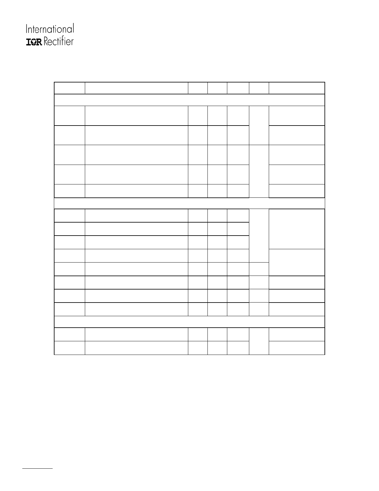
Electrical Characteristics (cont’d)
V
CC
= V
BS
= V
BIAS
=14 V +/- 0.25 V, C
LO
= C
HO
= C
PFC
= 1000 pF, R
FMIN
= 42.2 k
Ω, R
PH
= N/C, V
CPH
= V
VCO
= 0 V,
V
SD/EOL
= V
COMP
= V
CS
= V
OC
= V
BUS
= V
ZX
= 0 V, T
A
=25
o
C unless otherwise specified.
Symbol Definition Min
Typ
Max Units
Test
Conditions
PFC Error Amplifier Characteristics
I
COMP,
SOURCE
COMP pin OTA error amplifier output current
Sourcing
20 30 40
MODE = RUN
V
VBUS
= 3.5 V
V
COMP
=4.0 V
I
COMP,
SINK
COMP pin OTA error amplifier output current
Sinking
-40 -30 -20
µA
MODE = RUN
V
VBUS
= 4.5 V
V
COMP
=4.0 V
V
COMPOH
OTA error amplifier output voltage swing
(high state)
12.0 12.5 13.0
V
BUS
=3.5 V
I
COMP
=I
COMP
SOURCE-5
µA
V
COMPOL
OTA error amplifier output voltage swing
(low state)
0.2 0.4 0.5
V
BUS
=5.0 V
I
COMP
=I
COMP
SINK+5 µA
V
COMPFLT
OTA error amplifier output voltage in fault
mode
--- 0 ---
V
V
BUS
=4.0 V
PFC Control Characteristics
V
VBUSREG
V
BUS
internal reference voltage
3.9
4.0
4.1
V
VBUSOV
V
BUS
overvoltage comparator threshold
4.1
4.3
4.5
V
VBUSOV-
V
BUS
overvoltage fault reset threshold
4.0
4.15
4.3
V
COMP
= 4.0 V
V
ZX
ZX pin threshold voltage
1.8
2.0
2.2
V
V
ZXHYS
ZX pin comparator hysterisis
100
300
500
mV
V
ZXclamp
ZX pin clamp voltage (high state)
5.5
6.5
7.5
V
I
ZX
= 1 mA
t
BLANK
OC pin current-sensing blank time
---
300
---
ns
V
BUS
=4.0 V
V
COMP
=4.0 V
t
WD
PFC watch-dog pulse interval
150
400
500
µs
ZX = 0, V
COMP
= 4.0 V
PFC Protection Circuitry Characteristics
V
VBUSUV-
V
BUS
pin undervoltage reset threshold
2.7
3.0
3.3
V
OCTH+
OC pin over-current sense threshold
1.1
1.2
1.3
V
V
BUS
=V
COMP
=4.0 V
IRS2168D(S)PbF
www.irf.com Page 5
Electrical Characteristics (cont’d)
V
CC
= V
BS
= V
BIAS
=14 V +/- 0.25 V, C
LO
= C
HO
= C
PFC
= 1000 pF, R
FMIN
= 42.2 k
Ω, R
PH
= N/C, V
CPH
= V
VCO
= 0 V,
V
SD/EOL
= V
COMP
= V
CS
= V
OC
= V
BUS
= V
ZX
= 0 V, T
A
=25
o
C unless otherwise specified.
Symbol Definition Min
Typ
Max
Units
Test
Conditions
Ballast Control Oscillator Characteristics
f
OSC, RUN
Half-bridge oscillator run frequency
42.5
44.5
46.5
MODE = RUN
f
OSC, PH
Half-bridge oscillator preheat frequency
81
85
89
kHz
RPH = 42.2 k
Ω,
MODE = PREHEAT
D
Oscillator duty cycle
---
50
---
%
t
d
, LO
LO output deadtime
1.1
1.6
2.1
t
d
, HO
HO output deadtime
1.1
1.6
2.1
µs
V
FMIN
F
MIN
pin voltage
1.9
2.0
2.1
V
V
CC
= 14.0 V
Ballast Control Preheat, Ignition and Run Mode Characteristics
V
CPHEOP+
CPH pin end of preheat rising threshold
voltage
8.8 9.3 9.8
V
CPHSOI-
CPH pin start of ignition falling threshold
voltage
4.6 4.9 5.2
V
VCOPH
VCO pin preheat mode voltage
---
0
---
MODE = PREHEAT
V
VCOIGN
VCO pin ignition mode voltage
---
(Open
Drain)
---
V
MODE = IGNITION, V
CS
< V
CSTH+
I
VCOIGN
VCO pin ignition regulation discharge
current
--- 0.6 --- mA
MODE = IGNITION,
V
VCO
= 1 V,
V
CS
> V
CSTH+
V
CPHRUN+
CPH pin run mode rising threshold voltage
8.8
9.3
9.8
MODE = IGNITION
V
VCORUN
VCO pin run mode voltage
---
(Open
Drain)
---
V
MODE = RUN
Ballast Control Protection Circuitry Characteristics
V
CSTH+
CS pin over-current sense threshold
1.1
1.2
1.3
V
n
EVENTS
CS pin fault counter number of events
30
65
100
---
MODE = PREHEAT or
RUN
V
SDTH+
SD pin rising non-latched shutdown
threshold voltage
4.7 5.2 5.7
V
SDTH-
SD pin falling reset threshold voltage
2.5
3.0
3.5
V
EOLBIAS
EOL pin internal bias voltage
1.9
2.0
2.1
V
EOLTH+
EOL pin rising latched shutdown threshold
voltage
2.85
3.0
3.15
MODE = RUN
V
EOLTH-
EOL pin falling latched shutdown threshold
voltage
0.9 1.0 1.1
V
MODE = RUN
I
EOL, SOURCE
EOL pin OTA output sourcing current
---
10
---
MODE = PREHEAT
V
EOL
= 1.5 V
I
EOL,
SINK
EOL pin OTA output sinking current
---
-10
---
µA
MODE = PREHEAT
V
EOL
= 2.5 V
V
CPHFLT
CPH pin fault mode voltage
V
VCOFLT
VCO pin fault mode voltage
V
FMINFLT
FMIN pin fault mode voltage
---
0
---
V
MODE = FAULT
IRS2168D(S)PbF
www.irf.com Page 6
Electrical Characteristics (cont’d)
V
CC
= V
BS
= V
BIAS
=14 V +/- 0.25 V, C
LO
= C
HO
= C
PFC
= 1000 pF, R
FMIN
= 42.2 k
Ω, R
PH
= N/C, V
CPH
= V
VCO
= 0 V,
V
SD/EOL
= V
COMP
= V
CS
= V
OC
= V
BUS
= V
ZX
= 0 V, T
A
=25
o
C unless otherwise specified.
Gate Driver Output Characteristics (HO, LO and PFC pins)
V
OL
Low-level output voltage
---
COM
---
V
OH
High-level output voltage
---
V
CC
---
V
t
r
Turn-on rise time
---
120
220
t
f
Turn-off fall time
---
50
100
ns
I
0+
Source current
---
180
---
I
0-
Sink current
---
260
---
mA
Bootstrap FET Characteristics
V
B/ON
V
B
when the bootstrap FET is on
13.0
13.4
---
V
I
B/CAP
V
B
source current when FET is on
40
55
---
C
BS
=0.1 µF
I
B/10V
V
B
source current when FET is on
9
12
---
mA
V
B
=10 V
IRS2168D(S)PbF
www.irf.com Page 7
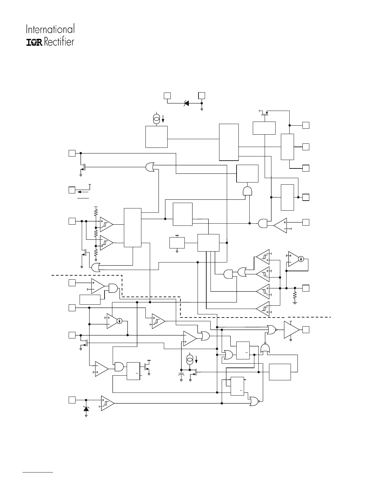
Schematic Block Diagram
PFC
COMP
ZX
6.5V
2V
Q
S
R2 Q
R1
Q
S
R
Q
VCC
OC
CPH
VCC
VCO
FMIN
COM
R
R
R
VBUS
VB
HO
VS
LO
CS
High-
Side
Driver
Low-
Side
Driver
1.2V
10
13
8
3
4
2
1
14
16
15
11
7
5
6
VCC
UVLO
400us
Watchdog
Timer
12
OVP
4.3V
65 Event
Fault
Counter
4.0V
VBUS
Under-Voltage
Reset
Gain
OTA1
Driver
and
Deadtime
Logic
15.6V
1.2V
Bootstrap
Control
VCC
RUN
200ns
Blank Time
IGN
R
SD/EOL
9
2V
5V
1V
3V
3V
Q
S
R
Q
VCC
3V
Ballast Control
PFC Control
VCC
IN
OUT
2V
2.0V
I
FMIN
R
RFMIN
I
FMIN
=
+/-10uA
Mode
Logic
PH
Ignition
Regulation
Fault
Logic
Oscillator
VCC
1M
Please Note: All values shown in block diagram are typical values only.
IRS2168D(S)PbF
www.irf.com Page 8
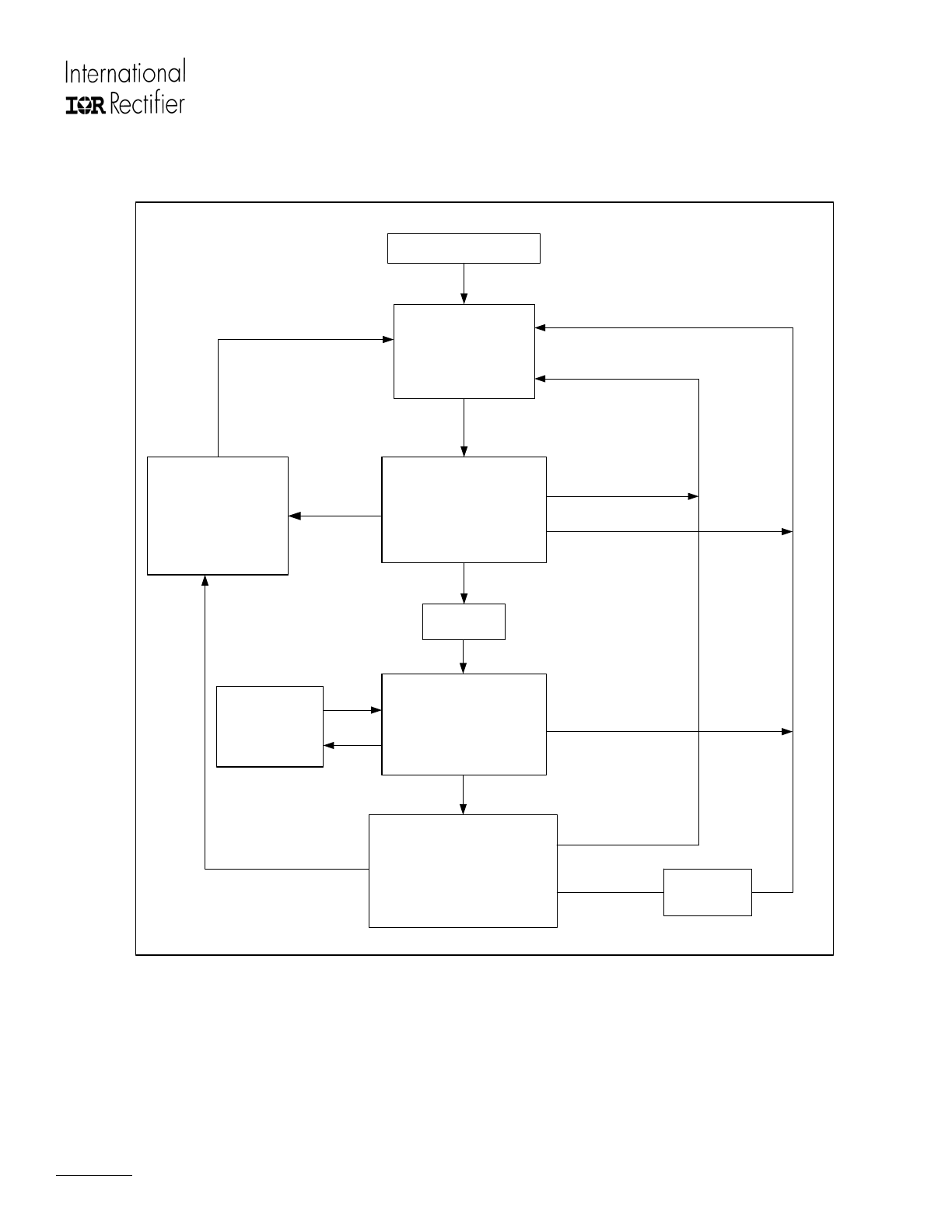
State Diagram
SD/EOL > 5.0 V (V
SDTH+
)
(Lamp Fault or Lamp Removal)
UVLO Mode
1
/
2
-Bridge Off
I
QCCUV
≅ 250 µA
CPH = 0 V
VCO = 0 V
PFC Off
PREHEAT Mode
1
/
2
-Bridge oscillating @ f
PH
V
CO
= 0 V
RPH // R
FMIN
CPH charging through RCPH
PFC Enabled (High Gain)
C
S
Fault Counter Enabled
V
CC
> 12.5 V (V
CCUV+
)
and
SD/EOL < 3.0 V (V
SDTH-
)
Power Turned On
FAULT Mode
Fault Latch Set
1
/
2
-Bridge Off
I
QCCFLT
≅ 400 µA
CPH = 0 V
V
CC
= 15.6V
V
CO
= 0 V
PFC Off
CS>1.2 V
(V
CSTH-)
SD/EOL > 5.0 V (V
SDTH+
)
(Lamp Removal)
or
V
CC
< 10.5 V (V
CCUV-
)
(Power Turned Off)
CPH > 9.3 V (V
CPHEOP+
)
(End of PREHEAT Mode)
IGNITION Mode
CPH charging through RCPH
VCO ramping up through RPH
f
PH
ramps to f
RUN
PFC = High Gain Mode
CS Fault Counter Disabled
Ignition Regulation Enabled
CS > 1.2 V (VCSTH+) for 65
events (nEVENTS)
or
SD/EOL < 1.0 V (V
EOLTH-
)
or
SD/EOL > 3.0 V (V
EOLTH+)
RUN Mode
VCO = 2 V
1/2-Bridge Oscillating @f
RUN
EOL Thresholds Enabled
PFC = Low Gain Mode
V
BUS UV
Threshold Enabled
C
S
Fault Counter Enabled
Ignition Regulation Disabled
V
BUS
< 3.0 V
(V
BUSUV-
)
CS > 1. 2V (V
CSTH+
)
for
65 events (n
EVENTS
)
Discharge V
CC
to UVLO
CPH > 9.3 V (V
CPHRUN
)
(End of IGNITION Mode)
CS Regulation
VCO discharged
slightly with 0.6 mA
current sink (IV
COIGN
)
C
S
<1.2 V
(V
CSTH+
)
CPH discharged
to CPHSOI-
CPH < 4.9 V (V
CPHSOI-
)
(Start of IGNITION Mode)
V
CC
< 10.5V (V
CCUV-
)
(V
CC
Fault or Power Down)
All values are typical.
Please refer to application diagram on page 1.
IRS2168D(S)PbF
www.irf.com Page 9
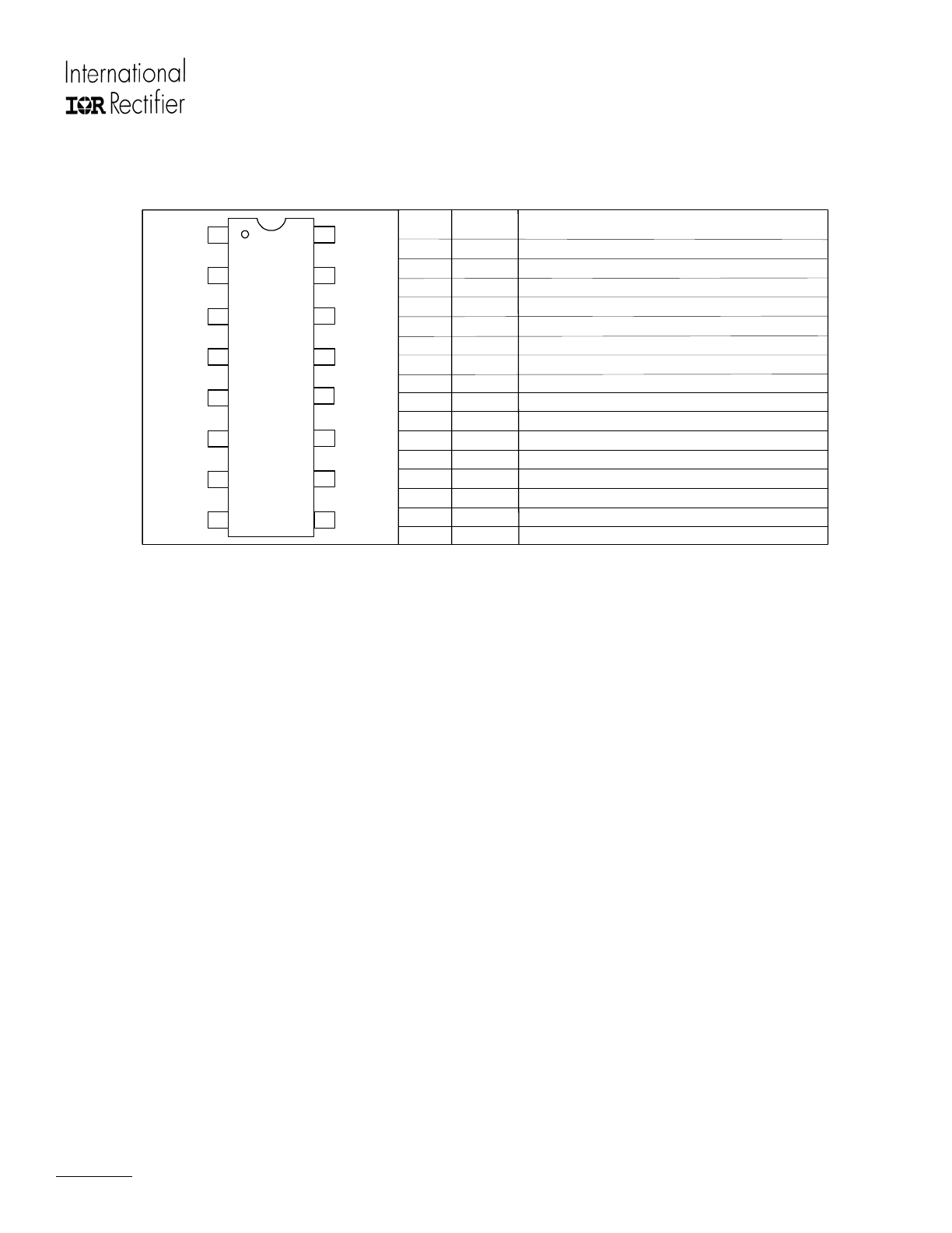
Lead Assignments & Definitions
Pin # Symbol
Description
1
3
7
6
5
4
2
VBUS
ZX
COMP
CPH
FMIN
VCO
Logic & low-side gate driver supply
DC bus sensing input
Voltage controlled oscillator/ignition ramp input
Oscillator minimum frequency setting
Preheat timing input
PFC error amplifier compensation
PFC
PFC zero-crossing detection
8
9
11
15
14
13
12
10
SD/EOL
VS
VB
VCC
COM
LO
CS
PFC gate driver output
IC power & signal ground
Shutdown/end of life sensing input
Half-Bridge current sensing input
Low-side gate driver output
High voltage floating return
High-side gate driver output
HO
High-side gate driver floating supply
16
15
14
13
12
11
IRS2168D
COM
VCC
VB
VS
HO
1
2
3
CPH
VBUS
4
5
7
VCO
COMP
FMIN
6
7
8
PFC
ZX
10
CS
LO
9
SD/EOL
16
OC
OC
PFC current sensing input
IRS2168D(S)PbF
www.irf.com Page 10
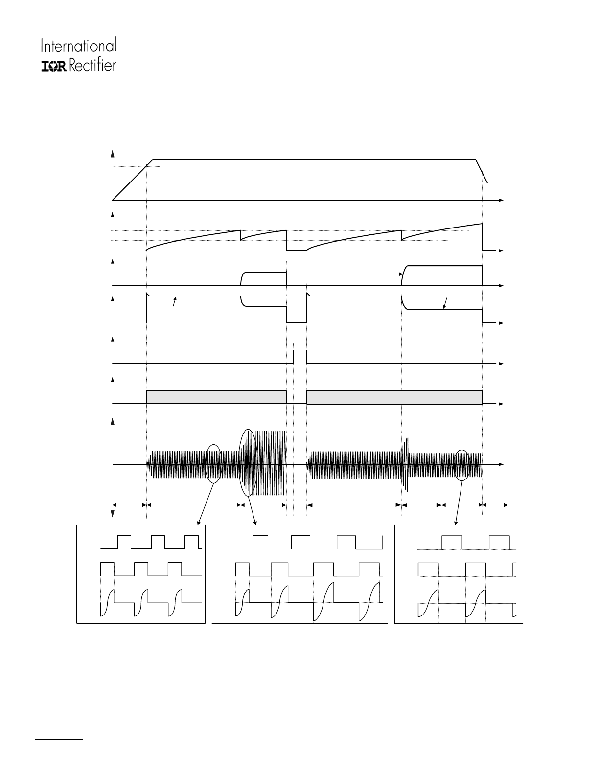
Timing Diagrams Ballast Section
VCC
HO, LO
UVLO+
15.6V
UVLO-
CPH
CS
PH
RUN
UVLO
UVLO
1.25V
FREQ
(2/3)*VCC
2V
f
ph
f
run
FAULT
PH
SD
>
5
V
SD
LO
CS
HO
LO
CS
HO
(1/3)*VCC
IGN
LO
CS
HO
IGN
1.25V
VCO
t
RAMP
=R
PH
*C
VCO
(RFMIN//RPH)
(RFMIN)