
- 1 -
JANUARY 18, 2013 |DATA SHEET | 3.6
1
IR3899
9A Highly Integrated SupIRBuck
TM
Single‐Input Voltage, Synchronous Buck Regulator
PD‐97661
78
80
82
84
86
88
90
92
94
96
98
0.9
1.8
2.7
3.6
4.5
5.4
6.3
7.2
8.1
9
Load Current (A)
Eff
ici
en
c
y
(%
)
1.2Vout
3.3Vout
12Vin,Internal bias,Frequency 600KHz
FEATURES
Single 5V to 21V application
Wide Input Voltage Range from 1.0V to 21V with
external Vcc
Output Voltage Range: 0.5V to 0.86× Vin
Enhanced Line/Load Regulation with Feed‐Forward
Programmable Switching Frequency up to 1.5MHz
Internal Digital Soft‐Start/Soft‐Stop
Enable input with Voltage Monitoring Capability
Thermally Compensated Current Limit with robust
hiccup mode over current protection
Smart internal LDO to improve light load and full
load efficiency
External Synchronization with Smooth Clocking
Enhanced Pre‐Bias Start‐Up
Precision Reference Voltage (0.5V+/‐0.5%) with
margining capability
Vp for Tracking Applications (Source/Sink Capability
+/‐9A)
Integrated MOSFET drivers and Bootstrap Diode
Thermal Shut Down
Programmable Power Good Output with tracking
capability
Monotonic Start‐Up
Operating temp: ‐40
o
C < Tj < 125
o
C
Small Size: 4mm x 5mm PQFN
Lead‐free, Halogen‐free and RoHS Compliant
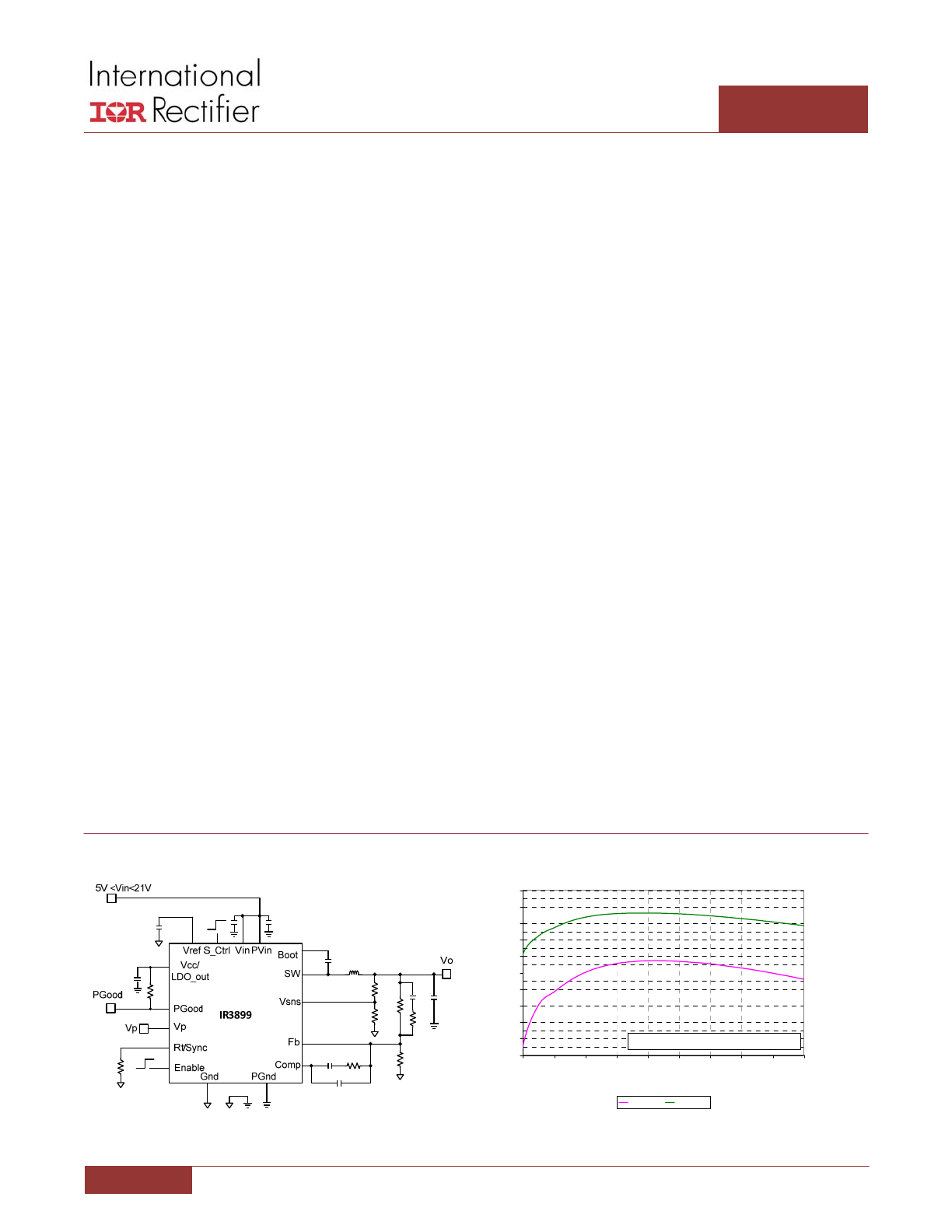
BASIC APPLICATION
Figure 1: IR3899 Basic Application Circuit
DESCRIPTION
The IR3899 SupIRBuck
TM
is an easy‐to‐use, fully integrated
and highly efficient DC/DC regulator. The onboard PWM
controller and MOSFETs make IR3899 a space‐efficient
solution, providing accurate power delivery.
IR3899 is a versatile regulator which offers programmable
switching frequency and the fixed internal current limit
while operates in wide input and output voltage range.
The switching frequency is programmable from 300kHz to
1.5MHz for an optimum solution.
It also features important protection functions, such as
Pre‐Bias startup, thermally compensated current limit,
over voltage protection and thermal shutdown to give
required system level security in the event of fault
conditions.
APPLICATIONS
Netcom Applications
Embedded Telecom Systems
Server Applications
Storage Applications
Distributed Point of Load Power Architectures
Figure 2: IR3899 Efficiency
- 2 -
JANUARY 18, 2013 |DATA SHEET | 3.6
2
IR3899
9A Highly Integrated SupIRBuck
TM
Single‐Input Voltage, Synchronous Buck Regulator
PD‐97661
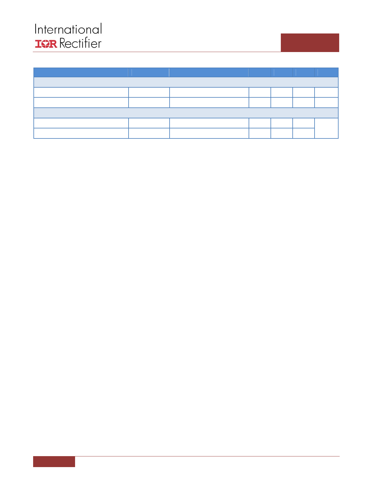
ORDERING INFORMATION
IR3899
―
Package
Tape & Reel Qty
Part Number
M
750
IR3899MTR1PBF
M
4000
IR3899MTRPBF
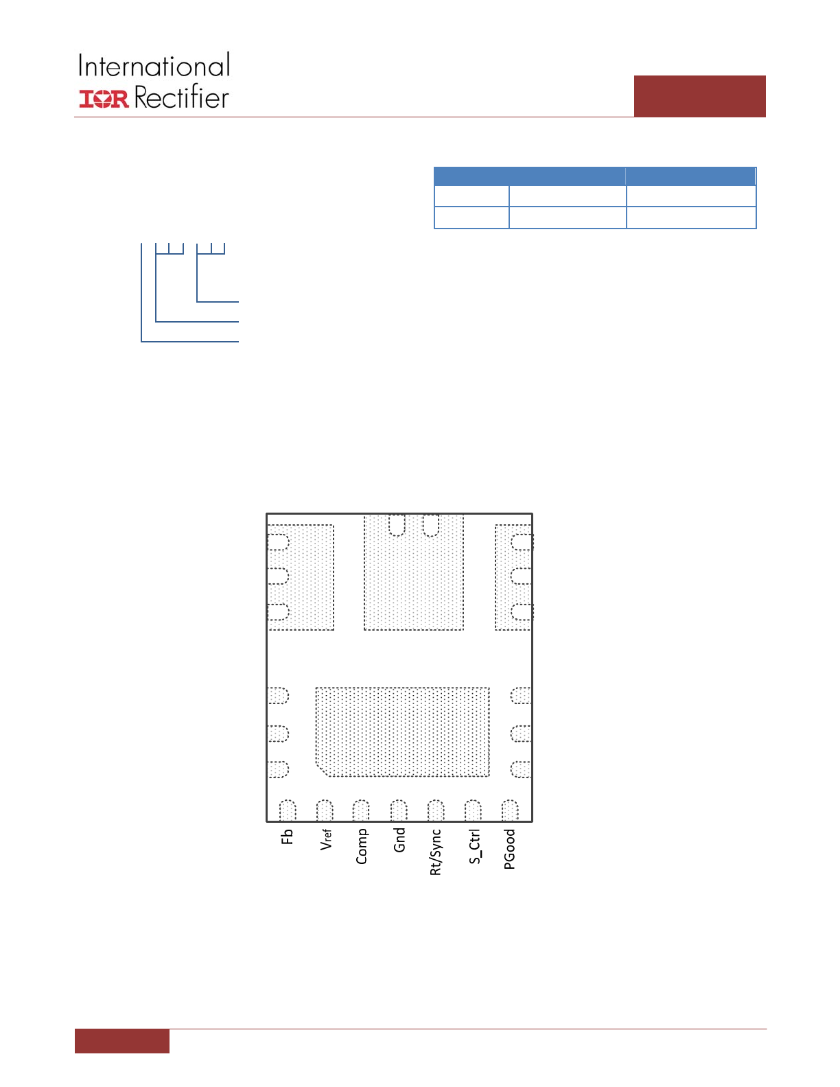
PIN DIAGRAM
4mm x 5mm POWER QFN
TOP VIEW
Enable
12
14
15
16
2
8
9
10
SW
3
4
5
6
1
7
V
sns
V
in
Vcc/LDO_Out
V
P
Boot
17
GND
13
PV
in
11
PGND
-
32
/
2
/
o
JA
o
J PCB
C W
C W
PBF
– Lead Free
TR/TR1 – Tape and Reel
M – Package Type
- 3 -
JANUARY 18, 2013 |DATA SHEET | 3.6
3
IR3899
9A Highly Integrated SupIRBuck
TM
Single‐Input Voltage, Synchronous Buck Regulator
PD‐97661
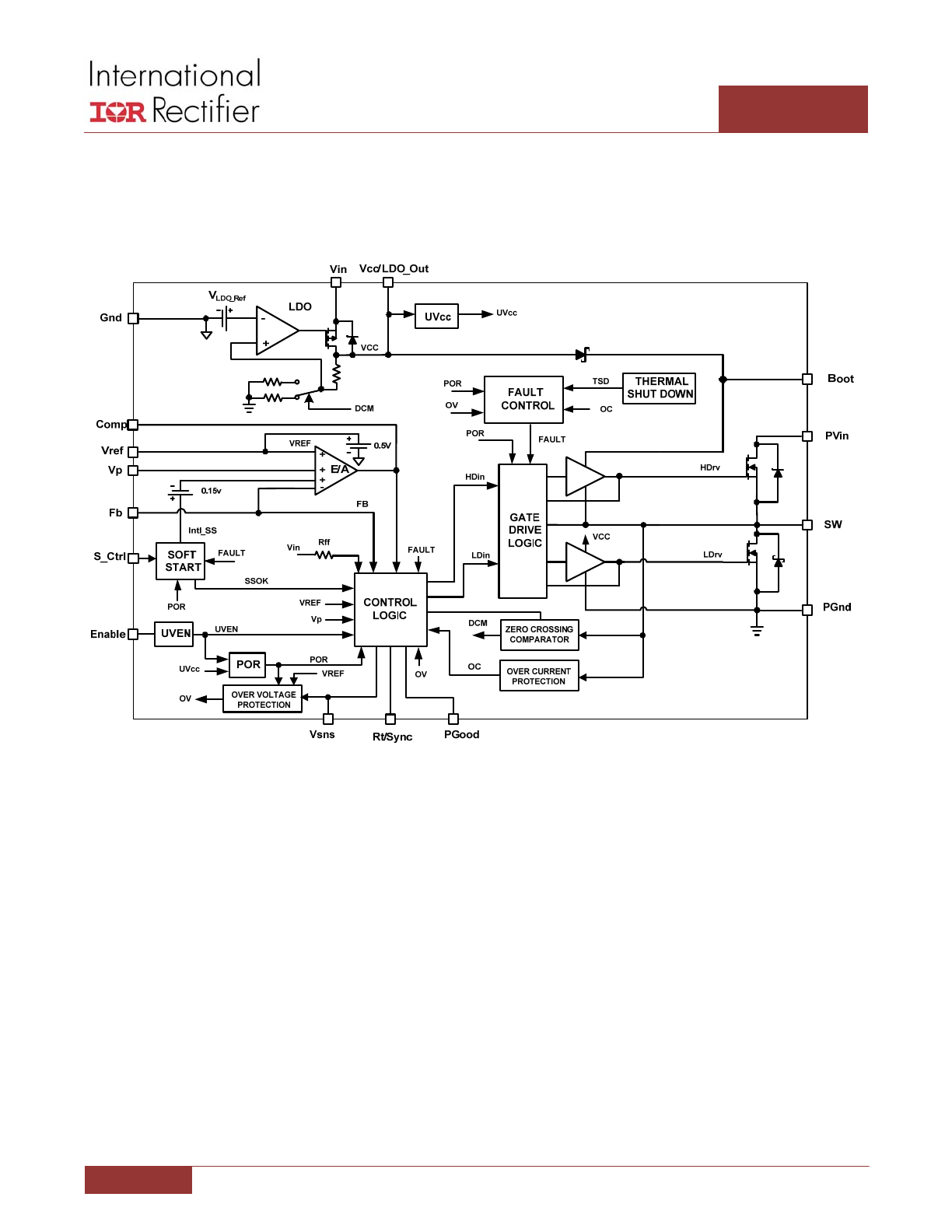
BLOCK DIAGRAM
Figure 3: IR3899 Simplified Block Diagram
- 4 -
JANUARY 18, 2013 |DATA SHEET | 3.6
4
IR3899
9A Highly Integrated SupIRBuck
TM
Single‐Input Voltage, Synchronous Buck Regulator
PD‐97661
PIN DESCRIPTIONS
PIN #
PIN NAME
PIN DESCRIPTION
1
Fb
Inverting input to the error amplifier. This pin is connected directly to the output
of the regulator via resistor divider to set the output voltage and provide
feedback to the error amplifier.
2
Vref
Internal reference voltage , it can be used for margining operation also. In
normal mode and sequencing mode, a 100pF ceramic capacitor is recommended
between this pin and Gnd. In tracking mode operation, Vref should be tied to
Gnd.
3
Comp
Output of error amplifier. An external resistor and capacitor network is typically
connected from this pin to Fb to provide loop compensation.
4
Gnd
Signal ground for internal reference and control circuitry.
5
Rt/Sync
Multi‐function pin to set switching frequency. Use an external resistor from this
pin to Gnd to set the free‐running switching frequency. An external clock signal
can be connected to this pin through a diode so that the device’s switching
frequency is synchronized with the external clock.
6
S_Ctrl
Soft start/stop control. A high logic input enables the device to go into the
internal soft start; a low logic input enables the output soft discharged. Pull this
pin to Vcc if this function is not used.
7
PGood
Power Good status pin. Output is open drain. Connect a pull up resistor (49.9k)
from this pin to the voltage lower than or equal to the Vcc.
8
Vsns
Sense pin for over‐voltage protection and PGood. It is optional to tie this pin to
FB pin directly instead of using a resistor divider from Vout.
9
Vin
Input voltage for Internal LDO. A 1.0µF capacitor should be connected between
this pin and PGnd. If external supply is connected to Vcc/LDO_Out pin, this pin
should be shorted to Vcc/LDO_out pin.
10
Vcc/LDO_Out
Input Bias for external Vcc Voltage/ output of internal LDO. Place a minimum
2.2µF cap from this pin to PGnd.
11
PGnd
Power Ground. This pin serves as a separated ground for the MOSFET drivers
and should be connected to the system’s power ground plane.
12
SW
Switch node. This pin is connected to the output inductor.
13
PVin
Input voltage for power stage.
14
Boot
Supply voltage for high side driver, a 100nF capacitor should be connected
between this pin and SW pin.
15
Enable
Enable pin to turn on and off the device, if this pin is connected to PVin pin
through a resistor divider, input voltage UVLO can be implemented.
16
Vp
Input to error amplifier for tracking purposes. In the normal operation, it is left
floating and no external capacitor is required. In the sequencing or the tracking
mode operation, an external signal can be applied as the reference.
17
Gnd
Signal ground for internal reference and control circuitry.
- 5 -
JANUARY 18, 2013 |DATA SHEET | 3.6
5
IR3899
9A Highly Integrated SupIRBuck
TM
Single‐Input Voltage, Synchronous Buck Regulator
PD‐97661
ABSOLUTE MAXIMUM RATINGS
Stresses beyond those listed under “Absolute Maximum Ratings” may cause permanent damage to the device. These are
stress ratings only and functional operation of the device at these or any other conditions beyond those indicated in the
operational sections of the specifications are not implied.
PVin, Vin
‐0.3V to 25V
VCC/LDO_Out
‐0.3V to 8V (Note 2)
Boot
‐0.3V to 33V
SW
‐0.3V to 25V (DC), ‐4V to 25V (AC, 100ns)
Boot to SW
‐0.3V to VCC + 0.3V (Note 1)
S_Ctrl, PGood
‐0.3V to VCC + 0.3V (Note 1)
Other Input/Output Pins
‐0.3V to +3.9V
PGnd to Gnd
‐0.3V to +0.3V
Storage Temperature Range
‐55°C to 150°C
Junction Temperature Range
‐40°C to 150°C (Note 2)
ESD Classification (HBM JESD22‐A114)
2kV
Moisture Sensitivity Level
JEDEC Level 2@260°C
Note 1: Must not exceed 8V
Note 2: Vcc must not exceed 7.5V for Junction Temperature between ‐10°C and ‐40°C
- 6 -
JANUARY 18, 2013 |DATA SHEET | 3.6
6
IR3899
9A Highly Integrated SupIRBuck
TM
Single‐Input Voltage, Synchronous Buck Regulator
PD‐97661
ELECTRICAL SPECIFICATIONS
RECOMMENDED OPERATING CONDITIONS FOR RELIABLE OPERATION WITH MARGIN
SYMBOL
MIN
MAX
UNITS
Input Voltage Range*
PVin
1.0
21
V
Input Voltage Range**
Vin
5
21
Supply Voltage Range***
V
CC
4.5
7.5
Supply Voltage Range
Boot to SW
4.5
7.5
Output Voltage Range
V
O
0.5
0.86xVin
Output Current Range
I
O
0
±9
A
Switching Frequency
F
S
300
1500
kHz
Operating Junction Temperature
T
J
‐40
125
°C
*Maximum SW node voltage should not exceed 25V.
**For internally biased single rail operation. When Vin drops below 6.8V, the internal LDO enters dropout. Please refer to Smart LDO
section and Over Current Protection for detailed application information.
*** Vcc/LDO_Out can be connected to an external regulated supply. If so, the Vin pin should be connected to Vcc/LDO_Out pin.
ELECTRICAL CHARACTERISTICS
Unless otherwise specified, these specifications apply over, 6.8V < Vin = PVin < 21V, Vref = 0.5V in 0°C < T
J
< 125°C.
Typical values are specified at T
a
= 25°C.
PARAMETER
SYMBOL
CONDITIONS
MIN
TYP
MAX
UNIT
Power Stage
Power Losses
P
LOSS
PVin=Vin
= 12V, V
O
= 1.2V,
I
O
= 9A, Fs = 600kHz, L = 0.51uH,
Vcc = 6.4V, Note 4
1.4
W
Top Switch
R
ds(on)_Top
VBoot ‐Vsw=6.4V,I
O
=9A, T
j
=25°C
17.5
22.5
mΩ
Bottom Switch
R
ds(on)_Bot
Vcc = 6.4V, I
O
= 9A, T
j
= 25°C
8.5
11.0
Bootstrap Diode Forward Voltage
I(Boot) = 10mA
180
260
470
mV
SW Leakage Current
I
SW
SW = 0V, Enable = 0V
1
µA
SW = 0V, Enable = high, Vp = 0V
Dead Band Time
T
db
Note 4
5
10
30
ns
Supply Current
VIN Supply Current (standby)
I
in(Standby)
EN = Low, No Switching
100
µA
VIN Supply Current (dynamic)
I
in(Dyn)
EN = High, Fs = 600kHz,
Vin = PVin = 21V
12
16
mA
Vcc/ LDO_ Out
Output Voltage
V
cc
Vin(min) = 6.8V, Icc = 0‐30mA,
Cload = 2.2uF, DCM = 0
6.0
6.4
6.7
V
Vin(min) = 6.8V, Icc = 0‐30mA,
Cload = 2.2uF, DCM = 1
4.0
4.4
4.8
LDO Dropout Voltage
V
cc_drop
Icc=30mA,Cload=2.2uF
0.7
V
Short Circuit Current
Ishort
70
mA
Zero‐crossing Comparator Delay
Tdly_zc
Note 4
256/Fs
s
- 7 -
JANUARY 18, 2013 |DATA SHEET | 3.6
7
IR3899
9A Highly Integrated SupIRBuck
TM
Single‐Input Voltage, Synchronous Buck Regulator
PD‐97661
PARAMETER
SYMBOL
CONDITIONS
MIN
TYP
MAX
UNIT
Zero‐crossing Comparator Offset
Vos_zc
Note 4
‐4
0
4
mV
Oscillator
Rt Voltage
Vrt
1.0
V
Frequency Range
F
s
Rt = 80.6K
270
300
330
kHz
Rt = 39.2K
540
600
660
Rt = 15.0K
1350
1500
1650
Ramp Amplitude
Vramp
Vin = 7.0V, Vin slew rate max =
1V/µs, Note 4
1.05
Vp‐p
Vin = 12V, Vin slew rate max =
1V/µs, Note 4
1.80
Vin = 21V, Vin slew rate max =
1V/µs, Note 4
3.15
Vcc=Vin = 5V, For external Vcc
operation, Note 4
0.75
Ramp Offset
Ramp(os)
Note 4
0.16
V
Min Pulse Width
Tmin(ctrl)
Note 4
60
ns
Max Duty Cycle
Dmax
Fs = 300kHz, PVin = Vin = 12V
86
%
Fixed Off Time
Toff
Note 4
200
250
ns
Sync Frequency Range
Fsync
270
1650
kHz
Sync Pulse Duration
Tsync
100
200
ns
Sync Level Threshold
High
3
V
Low
0.6
Error Amplifier
Input Offset Voltage
Vos_Vref
VFb – Vref, Vref = 0.5V
‐1.5
+1.5
%
Vos_Vp
VFb – Vp, Vp = 0.5V
‐1.5
+1.5
Input Bias Current
IFb(E/A)
‐1
+1
µA
Input Bias Current
IVp(E/A)
0
+4
Sink Current
Isink(E/A)
0.4
0.85
1.2
mA
Source Current
Isource(E/A)
4
7.5
11
mA
Slew Rate
SR
Note 4
7
12
20
V/µs
Gain‐Bandwidth Product
GBWP
Note 4
20
30
40
MHz
DC Gain
Gain
Note 4
100
110
120
dB
Maximum output Voltage
Vmax(E/A)
1.7
2.0
2.3
V
Minimum output Voltage
Vmin(E/A)
100
mV
Common Mode input Voltage
0
1.2
V
Reference Voltage
Feedback Voltage
Vfb
Vref and Vp pin floating
0.5
V
Accuracy
0°C < Tj < +70°C
‐0.5
+0.5
%
‐40°C < Tj < +125°C, Note 3
‐1.0
+1.0
- 8 -
JANUARY 18, 2013 |DATA SHEET | 3.6
8
IR3899
9A Highly Integrated SupIRBuck
TM
Single‐Input Voltage, Synchronous Buck Regulator
PD‐97661
PARAMETER
SYMBOL
CONDITIONS
MIN
TYP
MAX
UNIT
Vref Margining Voltage
Vref_marg
0.4
1.2
V
Sink Current
Isink_Vref
Vref = 0.6V
12.7
16.0
19.3
µA
Source Current
Isrc_Vref
Vref = 0.4V
12.7
16.0
19.3
Vref Comparator Threshold
Vref_disable
Vref pin connected externally
0.15
V
Vref_enable
0.4
Soft Start/Stop
Soft Start Ramp Rate
Ramp(SS_start)
0.16
0.2
0.24
mV/µs
Soft Stop Ramp Rate
Ramp(SS_stop)
‐0.24
‐0.2
‐0.16
S_Ctrl Threshold
High
2.4
V
Low
0.6
Power Good
PGood Turn on Threshold
VPG(on)
Vsns Rising, 0.4V < Vref < 1.2V
85
90
95
% Vref
Vsns Rising, Vref < 0.1V
85
90
95
% Vp
PGood Lower Turn off Threshold
VPG(lower)
Vsns Falling, 0.4V < Vref < 1.2V
80
85
90
% Vref
Vsns Falling, Vref < 0.1V
80
85
90
% Vp
PGood Turn on Delay
VPG(on)_Dly
Vsns Rising,see VPG(on)
1.28
ms
PGood Upper Turn off Threshold
VPG(upper)
Vsns Rising, 0.4V < Vref < 1.2V
115
120
125
% Vref
Vsns Rising, Vref < 0.1V
115
120
125
% Vp
PGood Comparator Delay
VPG(comp)_
Dly
Vsns < VPG(lower) or
Vsns >VPG(upper)
1
2
3.5
µs
PGood Voltage Low
PG(voltage)
IPgood
= ‐5mA
0.5
V
Tracker Comparator Upper
Threshold
VPG(tracker_
upper)
Vp Rising, Vref < 0.1V
0.4
V
Tracker Comparator Lower
Threshold
VPG(tracker_
lower)
Vp Falling, Vref < 0.1V
0.3
Tracker Comparator Delay
Tdelay(tracker)
Vp Rising, Vref < 0.1V,see
VPG(tracker_upper)
1.28
ms
Under‐Voltage Lockout
Vcc‐Start Threshold
V
CC
_UVLO_Start
Vcc Rising Trip Level
4.0
4.2
4.4
V
Vcc‐Stop Threshold
V
CC
_UVLO_Stop
Vcc Falling Trip Level
3.7
3.9
4.1
Enable‐Start‐Threshold
Enable_UVLO_Start
Supply ramping up
1.14
1.2
1.26
V
Enable‐Stop‐Threshold
Enable_UVLO_Stop
Supply ramping down
0.95
1
1.05
Enable Leakage Current
Ien
Enable = 3.3V
1
µA
Over‐Voltage Protection
OVP Trip Threshold
OVP_Vth
Vsns Rising, 0.45V < Vref < 1.2V
115
120
125
% Vref
Vsns Rising, Vref < 0.1V
115
120
125
% Vp
OVP Comparator Delay
OVP_Tdly
1
2
3.5
µs
- 9 -
JANUARY 18, 2013 |DATA SHEET | 3.6
9
IR3899
9A Highly Integrated SupIRBuck
TM
Single‐Input Voltage, Synchronous Buck Regulator
PD‐97661
PARAMETER
SYMBOL
CONDITIONS
MIN
TYP
MAX
UNIT
Over‐Current Protection
Current Limit
I
LIMIT
Tj = 25°C, Vcc = 6.4V
11
12.7
15.0
A
Hiccup Blanking Time
Tblk_Hiccup
Note 4
20.48
ms
Over‐Temperature Protection
Thermal Shutdown Threshold
Ttsd
Note 4
145
°C
Hysteresis
Ttsd_hys
Note 4
20
Note 3: Cold temperature performance is guaranteed via correlation using statistical quality control. Not tested in production.
Note 4: Guaranteed by design but not tested in production.
- 10 -
JANUARY 18, 2013 |DATA SHEET | 3.6
10
IR3899
9A Highly Integrated SupIRBuck
TM
Single‐Input Voltage, Synchronous Buck Regulator
PD‐97661
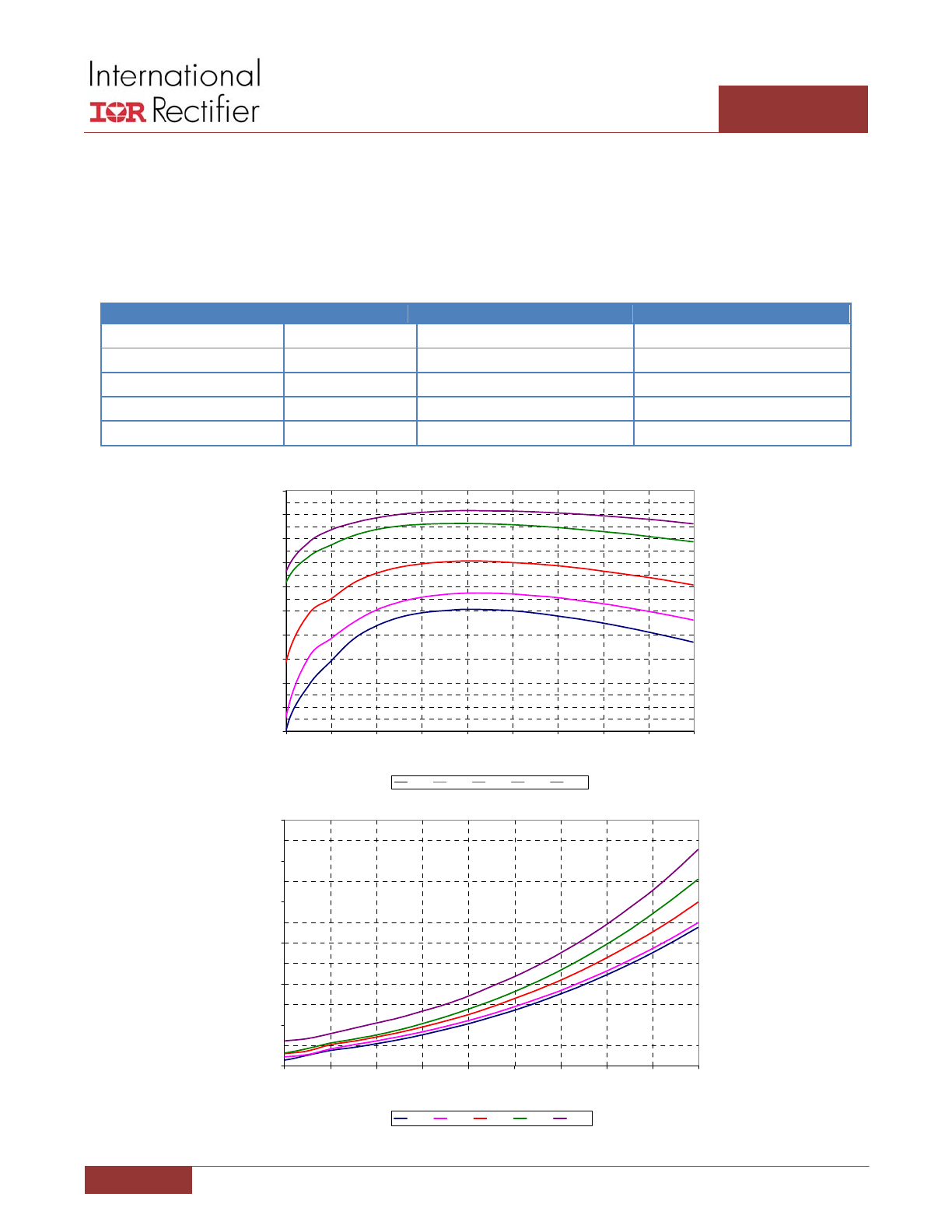
TYPICAL EFFICIENCY AND POWER LOSS CURVES
PVin = 12V, Vcc = Internal LDO (4.4V/6.4V), Io = 0A‐9A, Fs = 600KHz, Room Temperature, No Air Flow. Note that the
efficiency and power loss curves include the losses of IR3899, the inductor losses and the losses of the input and output
capacitors.
The table below shows the inductors used for each of the output voltages in the efficiency measurement.
VOUT (V)
LOUT (µH)
P/N
DCR (mΩ)
1.0
0.51
59PR9876N (Vitec)
0.29
1.2
0.51
59PR9876N (Vitec)
0.29
1.8
0.68
ETQP4LR68XFC (Panasonic)
1.58
3.3
1.2
MPL105‐1R2 (Delta)
2.9
5
1.2
MPL105‐1R2 (Delta)
2.9
78
80
82
84
86
88
90
92
94
96
98
0.9
1.8
2.7
3.6
4.5
5.4
6.3
7.2
8.1
9
Load Current (A)
Ef
fi
ci
ency (%
)
1.0V
1.2V
1.8V
3.3V
5.0V
0.2
0.6
1
1.4
1.8
2.2
2.6
0.9
1.8
2.7
3.6
4.5
5.4
6.3
7.2
8.1
9
Load Current (A)
Power
Loss
(W)
1.0V
1.2V
1.8V
3.3V
5.0V