
IR3710MTRPBF
Page 1 of 20
www.irf.com
IR Confidential
4/26/10
WIDE INPUT AND OUTPUT, SYNCHRONOUS BUCK REGULATOR
FEATURES
Input Voltage Range: 3V to 28V
Output Voltage Range: 0.5V to 12V
Constant On-Time control
Excellent Efficiency at very low output current levels
Gate drive charge pump option to maximize
efficiency at higher output current levels
Compensation Loop not Required
Programmable switching frequency, soft start, and
over current protection
Power Good Output
Precision Voltage Reference (0.5V, +/-1%)
Enable Input with Voltage Monitoring Capability
Pre-bias Start Up
Under/Over Voltage Fault Protection
16pin 3x3 MLPQ lead free package
RoHS compliant
DESCRIPTION
The IR3710 is a single-phase sync-buck PWM
controller optimized for efficiency in high performance
portable electronics. The switching modulator uses
constant on-time control. Constant on-time with diode
emulation provides the highest light-load efficiency
required for all.
Programmable switching frequency, soft start, and over
current protection allows for a very flexible solution
suitable for many different applications. The
combination of the gate drive charge pump option and
constant on time control allow efficiency optimization in
the whole output current range, making this device an
ideal choice for battery powered applications.
Additional features include pre-bias startup, very
precise 0.5V reference, over/under voltage shut down,
power good output, and enable input with voltage
monitoring capability.
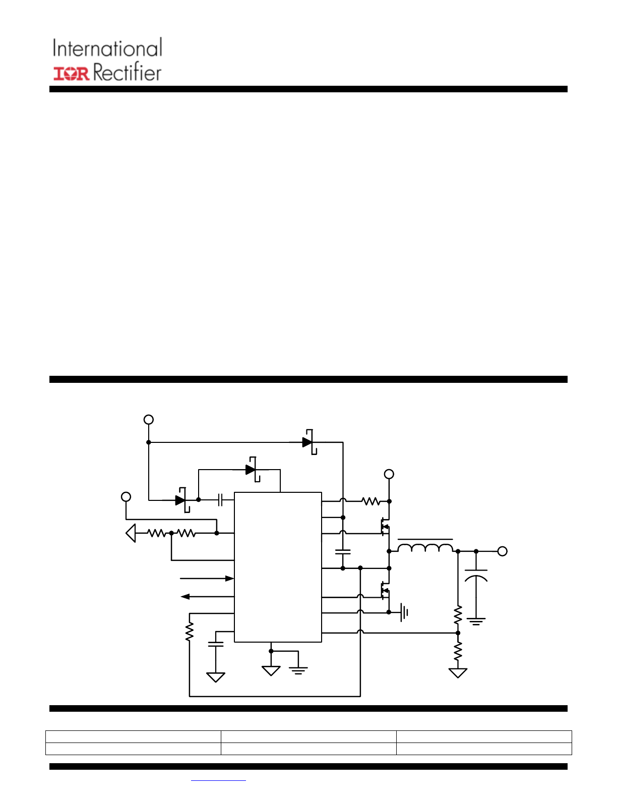
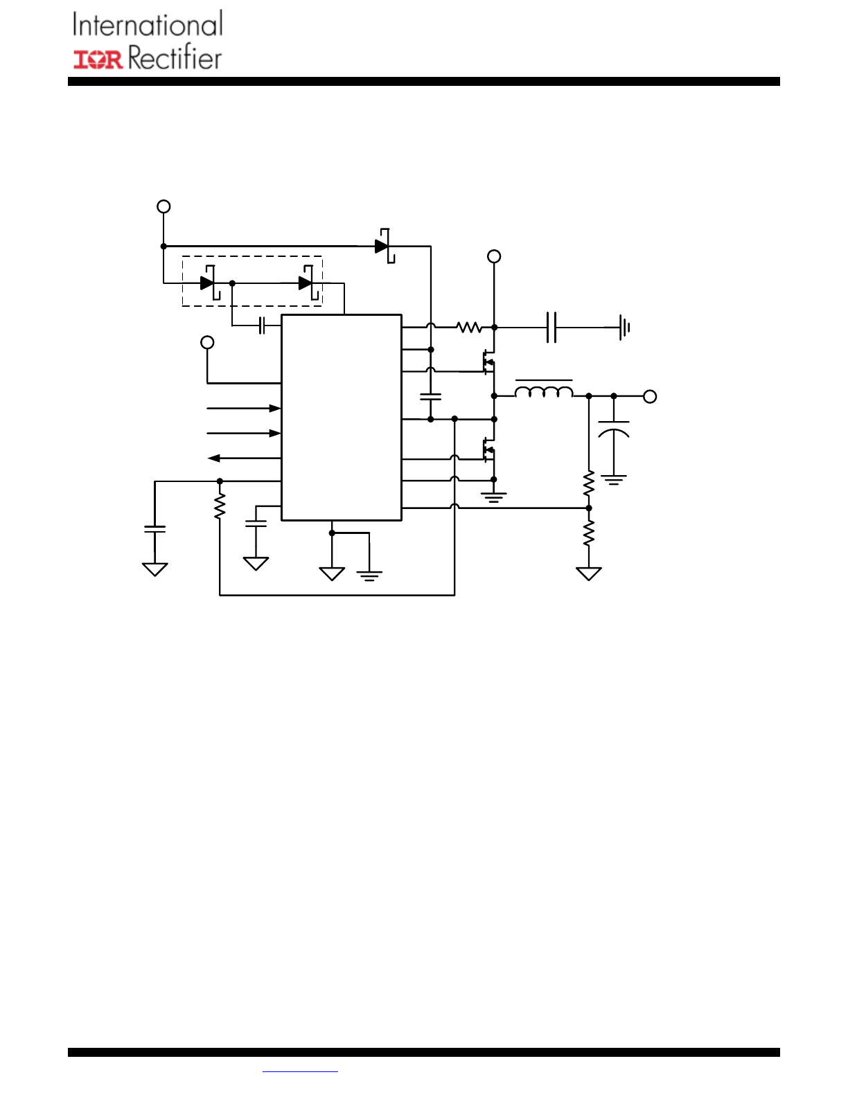
APPLICATION CIRCUIT
Enhanced Gate Drive Application Circuit:
IR3710
BOOT
UGATE
PHASE
LGATE
EN
FB
PVCC
PGND
FF
ISET
VCC
GND
SS
FCCM
PGOOD
CPO
V5
V3.3
D1
D2
C1
R
FF
R
ISET
C
SS
C
BOOT
C
OUT
L
R
1
R
2
D
BOOT
V
IN
V
OUT
10k
6.2k
ORDERING INFORMATION
Package Description
Pin Count
Parts Per Reel
IR3710MTRPbF 16
4000
Data Sheet No. PD60367
IR3710MTRPBF
Page 2 of 20
www.irf.com
IR Confidential
4/26/10
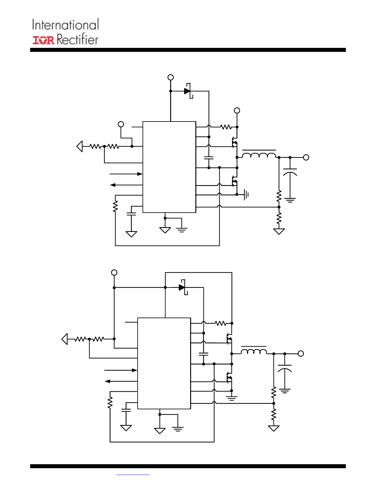
Fix Gate Voltage Application Circuit:
IR3710
BOOT
UGATE
PHASE
LGATE
EN
FB
PVCC
PGND
FF
ISET
VCC
GND
SS
FCCM
PGOOD
CPO
V5
V3.3
R
FF
R
ISET
C
SS
C
BOOT
C
OUT
L
R
1
R
2
D
BOOT
V
IN
V
OUT
10k
6.2k
NC
3.3V Input Voltage Application Circuit:
V
OUT
IR3710
BOOT
UGATE
PHASE
LGATE
EN
FB
PVCC
PGND
FF
ISET
VCC
GND
SS
FCCM
PGOOD
CPO
V3.3
R
FF
R
ISET
C
SS
C
BOOT
C
OUT
L
R
1
R
2
D
BOOT
NC
10k
6.2k
IR3710MTRPBF
Page 3 of 20
www.irf.com
IR Confidential
4/26/10
ABSOLUTE MAXIMUM RATINGS
Absolute Maximum Ratings (Referenced to GND)
BOOT Voltage: ................................................40 V
PHASE Voltage:....-5V(100ns),-0.3V(DC) to 32.5 V
FF, ISET:..........................................................32 V
BOOT minus PHASE Voltage:........................7.5 V
PVCC: ............................................................7.5 V
VCC:................................................................3.9 V
PGOOD:..........................................................3.9 V
PGND to GND:................................... -0.3V to 0.3V
All other pins ...................................................3.9 V
Operating Junction Temperature .. -10°C to +150
o
C
Storage Temperature Range .......... -65
o
C to 150
o
C
ESD Rating ...............................................Class 1C
MSL Rating ..................................................Level 2
Stresses beyond those listed under “Absolute Maximum Ratings” may cause permanent damage to the device.
These are stress ratings only and functional operation of the device at these or any other conditions beyond those
indicated in the operational sections of the specifications are not implied.
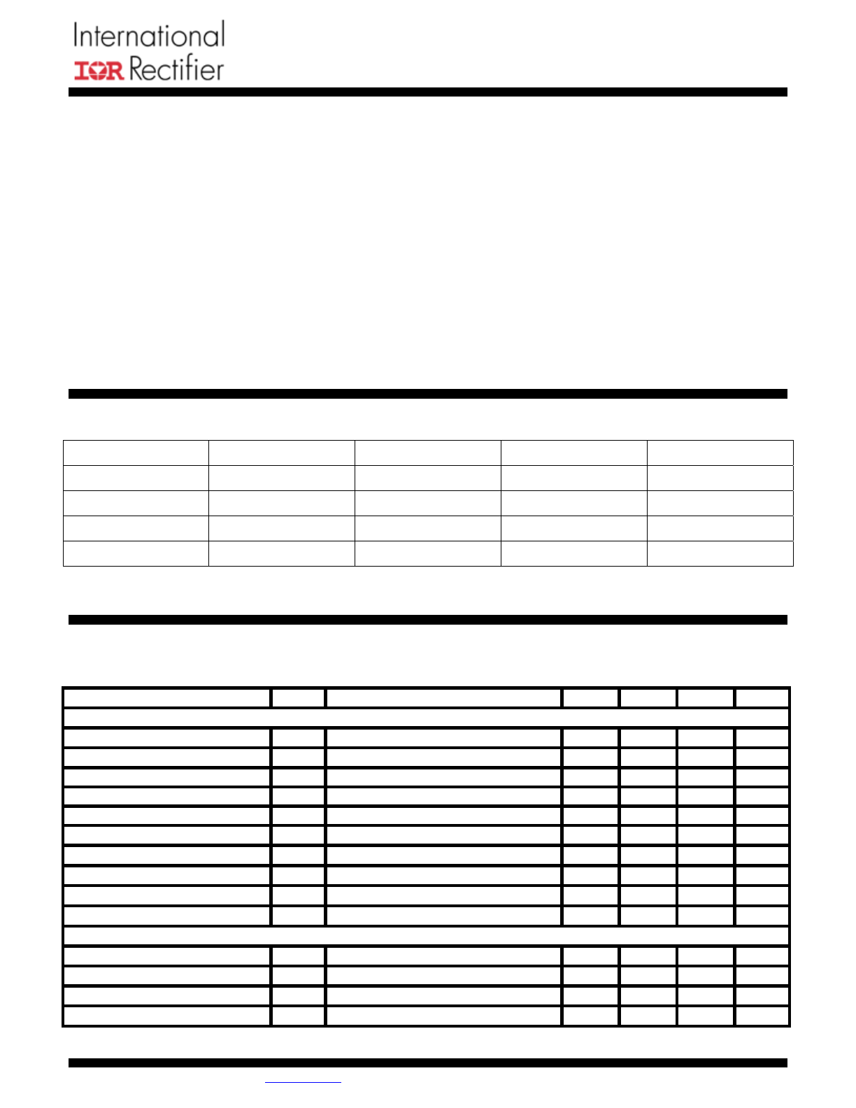
RECOMMENDED OPERATING CONDITIONS
Symbol Definition Min
Max
Units
V
IN
Input
Voltage 3 28*
V
BOOT to PHASE
Supply Voltage
7.0
V
V
OUT
Output
Voltage
0.5 12
V
Fs Switching
Frequency
1000
kHz
* Note: PHASE pin must not exceed 32.5V.
ELECTRICAL SPECIFICATIONS
Unless otherwise specified, these specifications apply: VCC = 3.3V, PVCC = 7.0V, 0
o
C ≤
T
J
≤ 125
o
C
PARAMETER NOTE TEST
CONDITION MIN
TYP
MAX
UNIT
BIAS SUPPLIES
VCC Turn-on Threshold
3
V
VCC Turn-off Threshold
2.65
V
VCC Threshold Hysterisis
60
mV
PVCC Turn-on Threshold
3.05
V
PVCC Turn-off Threshold
2.65
V
PVCC Threshold Hysterisis
60
mV
VCC Shutdown Current
EN=LOW
25
μA
VCC Operating Current
EN=HIGH, No gate loading
1.2
mA
PVCC Shutdown Current
EN=LOW; PVCC = 5V
20
μA
FF Shutdown Current
EN=LOW
2
μA
CONTROL LOOP
Reference Accuracy, V
REF
V
FB
=
0.5V
0.495 0.5 0.505 V
On-Time Accuracy
R
FF
= 180K, V
IN
= 12.6V
270
300
330
ns
Zero Current Threshold
Measure at V
PHASE
-4.5
4.5
mV
Soft-Start Current
FCCM = EN = HIGH
8
10
12
μA
IR3710MTRPBF
Page 4 of 20
www.irf.com
IR Confidential
4/26/10
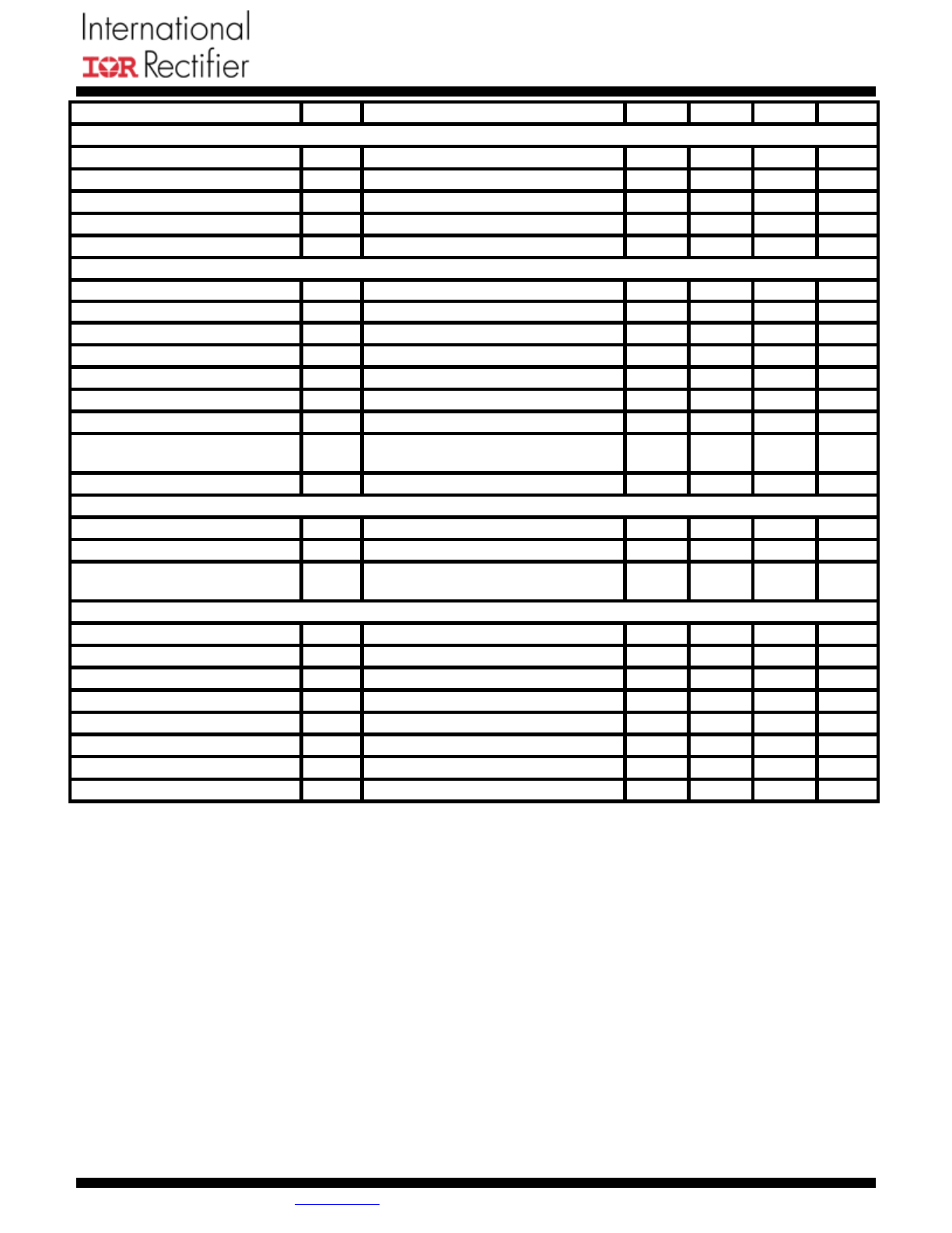
NOTES:
1.
Guaranteed by design, not tested in production
PARAMETER NOTE TEST
CONDITION MIN
TYP
MAX
UNIT
FAULT PROTECTION
ISET pin output current
18
20
22
μA
Under Voltage Threshold
Falling V
FB
& monitor PGOOD
0.37
0.4
0.43
V
Under Voltage Hysteresis
Rising V
FB
7.5 mV
Over Voltage Threshold
Rising V
FB
& monitor PGOOD
0.6
V
PGOOD Delay Threshold (V
SS
)
0.6 V
GATE DRIVE
UGATE Source Resistance
1
I
GATE
= 0.1A
1.5
3
Ω
UGATE Sink Resistance
1
I
GATE
= 0.1A
1
2
Ω
UGATE Rise and Fall Time
3nF load; 1V & 4V thresholds
10
ns
LGATE Source Resistance
1
I
GATE
= 0.1A
1.5
3
Ω
LGATE Sink Resistance
1
I
GATE
= 0.1A
0.4
1
Ω
LGATE Rise Time
6.8nF load; 1V to 4V
15
ns
LGATE Fall Time
6.8nF load; 4V to 1V
10
ns
Dead time
Measure time from
V
LGATE
= 1V to V
UGATE
= 1V
5 50
ns
Minimum LGATE Interval
400
ns
CHARGE PUMP OUTPUT
Source Resistance
I
CPO
=15mA
3.3
5
Ω
Sink Resistance
I
CPO
=15mA
1
2.1
Ω
Charge Pump Disable
Threshold, V
CP TH
FCCM = HIGH
6.8
7.2
V
LOGIC INPUT AND OUTPUT
EN Rising Threshold
1.14
1.22
1.3
V
EN
Hysterisis
40 100 160 mV
EN Input Current
1
μA
FCCM Rising Threshold
1
1.2
V
FCCM Falling Threshold
0.5
0.7
V
FCCM
Hysterisis
0.3
FCCM Input Current
1
μA
PGOOD pull down resistance
I
PGOOD
=2mA
50
100
Ω
IR3710MTRPBF
Page 5 of 20
www.irf.com
IR Confidential
4/26/10
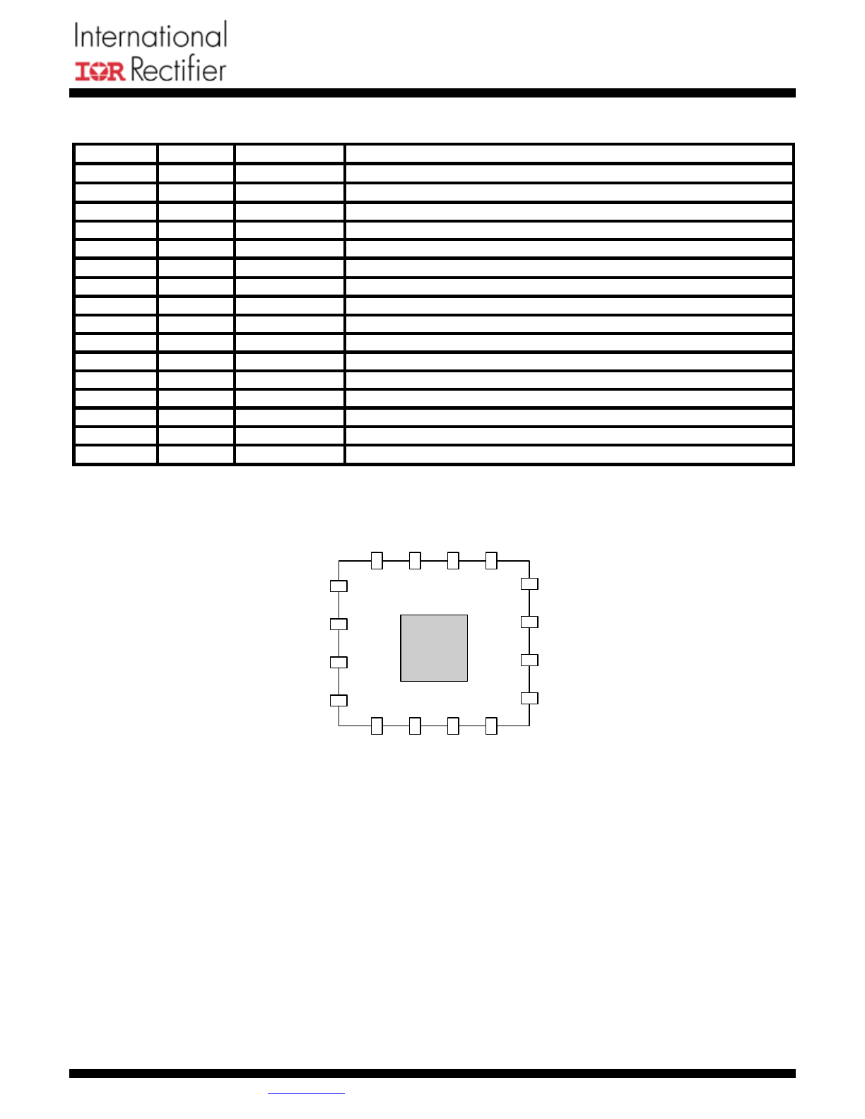
IC PIN ORDER AND DESCRIPTION
NAME NUMBER
I/O
LEVEL DESCRIPTION
BOOT 1
V
IN
+PVCC
Bootstrapped gate drive supply – connect a capacitor to PHASE
FF 2
V
IN
Input voltage feed forward – sets on-time with a resistor to V
IN
EN
3
3.3V
Enable input; EN = LOW inhibits GATE pulses
ISET 4
32V
Current limit setting with a resistor to PH pin
PGOOD
5
3.3V
Power good – pull up to 3.3V
GND 6
Reference
Bias return and signal reference
FCCM
7
3.3V
Force continuous conduction mode when pulled up to VCC
FB 8
3.3V
Feedback input
SS
9
3.3V
Set soft start slew-rate with a capacitor to GND
VCC 10
3.3V IC
bias
supply
CPO 11
3.3V Charge
Pump
Output
PVCC
12
7.4V
Gate drive supply
LGATE
13
PVCC
Lower gate drive for synchronous MOSFET
PGND
14
Reference
Power return – connect to source of synchronous MOSFET
PHASE 15
V
IN
Phase node (or switching node) of MOSFET half bridge
UGATE 16
V
IN
+ V5
Upper gate drive for control MOSFET
UG
AT
E
PHASE
PGND
LG
AT
E
EN
BOOT
FF
PVCC
CPO
VCC
GND
FB
ISET
SS
FCCM
PGOOD
1
2
3
4
5
6
7
8
12
11
10
9
16
15
14
13
GND
θ
JA
= 49
o
C/W
θ
JC
= 4
o
C/W
IR3710MTRPBF
Page 6 of 20
www.irf.com
IR Confidential
4/26/10
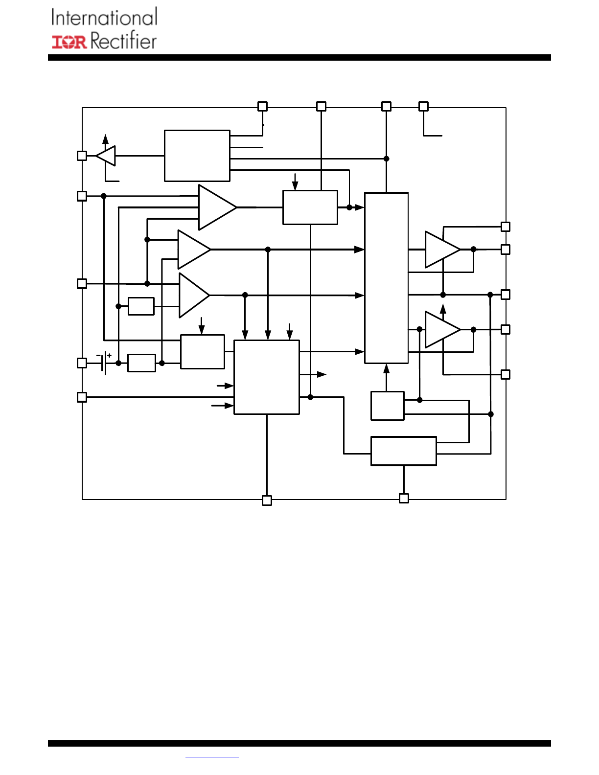
BLOCK DIAGRAM
SSDelay
PWM
BOOT
UGATE
PHASE
LGATE
GATE
DRIVE
LOGIC
PGND
ON-TIME
FF
+
-
SOFT
START
SS
Run
+
EN
PGOOD
FB
VCC
GND
ISET
FCCM
CONTROL
LOGIC
POR
+
-
V
REF
x0.8
OVER
CURRENT
OC#
FF
x1.2
UV#
CPO
VCC
VCC
PGND
PVCC
FCCM
FF
VCC
PVCC
PWM
COMP
SET
PVCC
Charge
Pump
Regulator
ZCROSS
Run
+
-
OV
PVCC
Run
DCM
ZCROSS
IR3710MTRPBF
Page 7 of 20
www.irf.com
IR Confidential
4/26/10
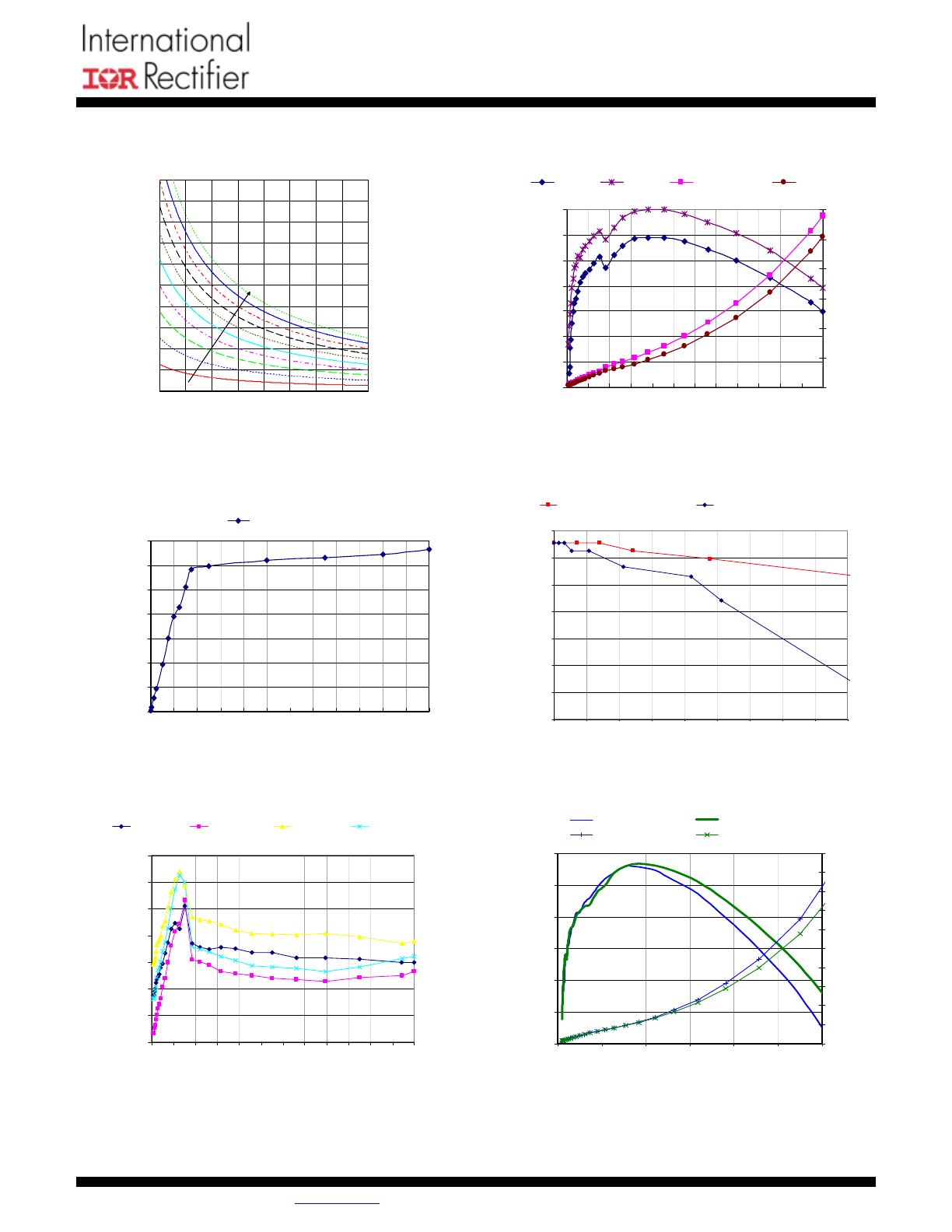
TYPICAL OPERATING DATA
(Circuit of Figure 18, VCC = 3.3V, V5 = 5V, V
IN
= 12.6V, Unless otherwise noted.)
Figure 1. Feedforward Resistance vs Switching Freq:
0.5V V
OUT
step, FCCM = HIGH.
0
50
100
150
200
250
300
350
0
2
4
6
8
10 12 14 16 18 20 22 24
Output Current (A)
S
w
itc
hi
ng
F
requenc
y (
K
H
z
Freq vs Load
Figure 2. Switching Frequency vs Output Current
1.09800
1.09850
1.09900
1.09950
1.10000
1.10050
1.10100
1.10150
0
2
4
6
8
10 12 14 16 18 20 22 24
Output Current(A)
V
o
u
t(V
)
12Vin@0C
12Vin@65C
19Vin@0C
19Vin@65C
Figure 3. Output Voltage Regulation versus Input
Voltage and Ambient Temperature
76
78
80
82
84
86
88
90
0
2
4
6
8 10 12 14 16 18 20 22 24
Output Current(A)
E
ff
ici
e
n
cy
(
%
0.0
1.0
2.0
3.0
4.0
5.0
6.0
Po
w
e
r L
o
s
s
(
W
)
19Vin
12Vin
Ploss-19Vin
Ploss-12Vin
Figure 4. System Efficiency
6
6.2
6.4
6.6
6.8
7
7.2
7.4
0
5
10
15
20
25
30
35
40
45
Gate Charge (nC)
PV
C
C
(
V
)
Fs =300kHz; Ccpo=1uF
Fs=1.34MHz ;Ccpo=1uF
Figure 5. Charge Pump Regulation
78
80
82
84
86
88
90
0
2
4
6
8
10
12
Output Current(A)
E
ff
ici
en
cy
(
%
0.0
0.5
1.0
1.5
2.0
2.5
3.0
3.5
4.0
4.5
5.0
P
o
w
er
L
o
ss
(W)
5V Drive
Enhanced Gate
Ploss-5V Drive
Ploss-Enhanced Gate
Figure 6. Charge Pump Efficiency Comparison:
1.25Vout, 12.6Vin, 300kHz,
IRF8721/8721, 0.82uH (4.2mOhm DCR)
Switching Frequency
F
eedf
o
rw
ar
d Resistance
1000000
000000
Rff 0.5 fsw
,
(
)
Rff 1 fsw
,
(
)
Rff 1.5 fsw
,
(
)
Rff 2 fsw
,
(
)
Rff 2.5 fsw
,
(
)
Rff 3 fsw
,
(
)
Rff 3.5 fsw
,
(
)
Rff 4 fsw
,
(
)
Rff 4.5 fsw
,
(
)
Rff 5 fsw
,
(
)
1000000
200000
fsw
Switching Frequency (KHz)
Feedf
or
w
ard
R
esistance (K
Ω
)
200
1000
0
1000
V
OUT
= 0.5V
V
OUT
= 5V
IR3710MTRPBF
Page 8 of 20
www.irf.com
IR Confidential
4/26/10
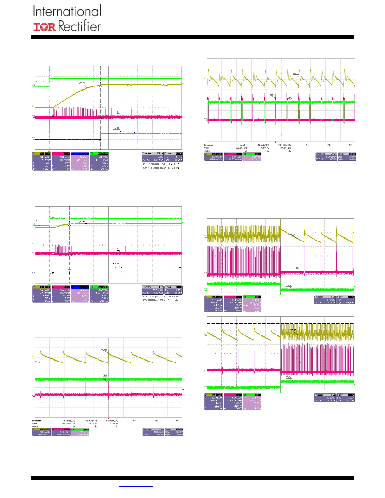
TYPICAL OPERATING WAVEFORM
(Circuit of Figure 18, VCC = 3.3V, V5 = 5V, V
IN
= 12.6V, Unless otherwise noted.)
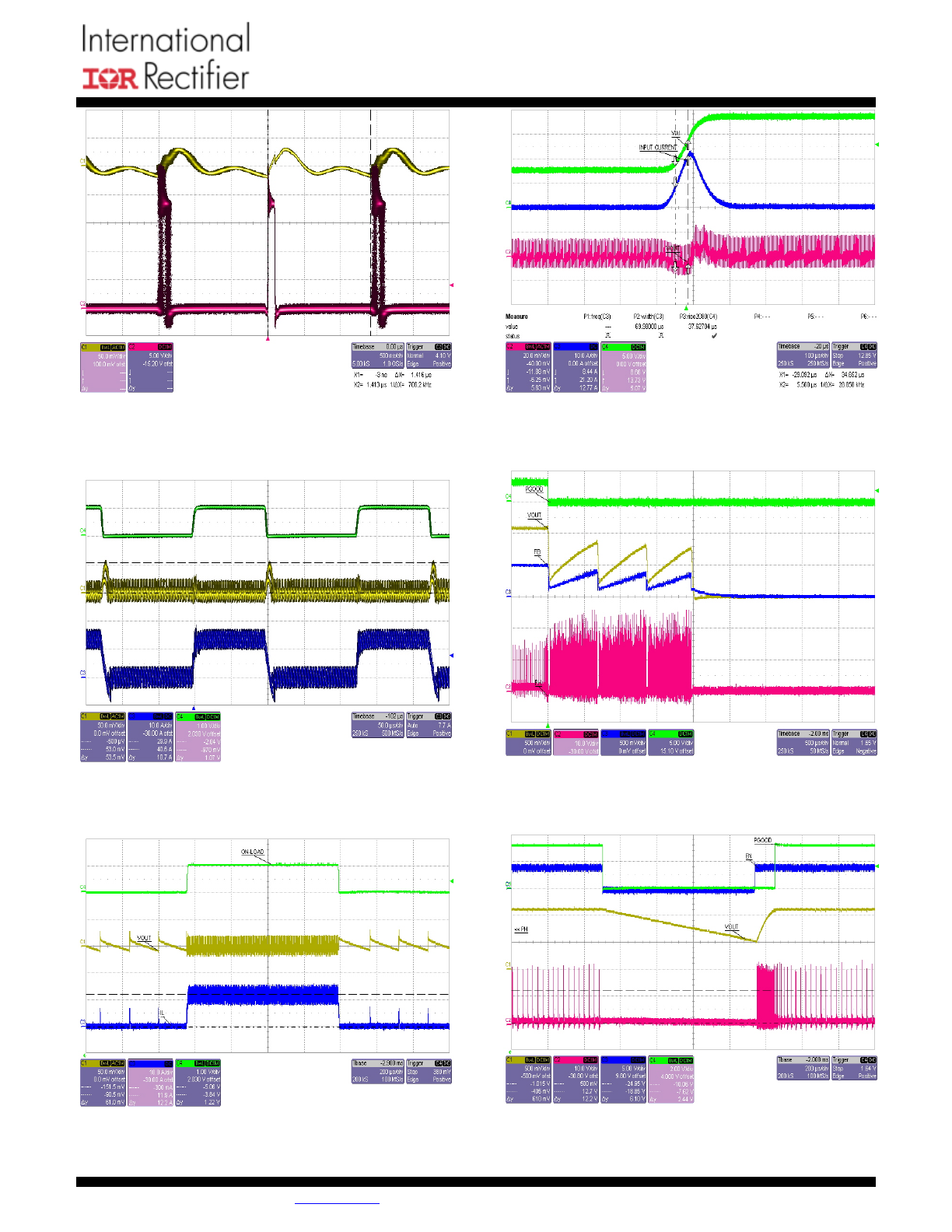
CH1:Vout(0.5V/div), CH2: PHASE (20V/div)
CH3: PGOOD(5V/div), CH4:EN(5V/div) ; 50uS/div
Figure 7. Start up with FCCM = Low @ 30mA
CH1:Vout(0.5V/div), CH2: PHASE (20V/div)
CH3: PGOOD(5V/div), CH4:EN(5V/div) ; 50uS/div
Figure 8. Start up with Prebias Vout, FCCM = Low @ 30mA
CH1:Vout(20mV/div), CH2: PHASE (5V/div), CH4:
CPO(2V/div) ; 100uS/div
Figure 9. Charge Pump Off in DCM
CH1:Vout(20mV/div), CH2: PHASE (5V/div)
CH4: CPO(2V/div) ; 5uS/div
Figure 10. Charge Pump ON
CH1:Vout(20mV/div), CH2: PHASE (5V/div)
CH4: FCCM(5V/div) ; 100uS/div
Figure 11. DCM/FCCM Transition
IR3710MTRPBF
Page 9 of 20
www.irf.com
IR Confidential
4/26/10
CH1:Vout(50mV/div), CH2: PHASE (5V/div);50uS/div
Figure 12. Frequency Variation less than 10% at 20A Load
CH1:Vout(50mV/div), CH3: Inductor Current (10A/div),
CH4: On-Board Load: 0A-14A ;50uS/div
Figure 13. Load Step Transient in CCM @ Vin = 19V
CH1:Vout(50mV/div), CH3: Inductor Current (10A/div),
CH4: On-Board Load: 0.1A-12A; 50uS/div
Figure 14. Load Step Transient in DCM @ Vin = 19V
CH2:Vout(20mV/div), CH3: Input Current (10A/div), CH4:
Input Voltage (5V/div) 8V to 19V; 100uS/div
Figure 15. Input Voltage Step at 2A Load with 0.1V/uS
CH1:Vout(0.5V/div), CH2: PHASE (10V/div), CH3: FB
(0.5V/div), CH4: PGOOD (5V/div); 500uS/div
Figure 16. Over Current Protection at 30A
CH1:Vout(0.5V/div), CH2: PHASE (10V/div), CH3: EN
(5V/div), CH4: PGOOD (2V/div); 200uS/div
Figure 17. Shutdown by EN in DCM @500mA
IR3710MTRPBF
Page 10 of 20
www.irf.com
IR Confidential
4/26/10
TYPICAL OPERATING CIRCUIT
IR3710
BOOT
UGATE
PHASE
LGATE
EN
FB
PVCC
PGND
FF
ISET
VCC
GND
SS
FCCM
PGOOD
CPO
V5
V3.3
D1
D2
1uF
5.11K
2.2nF
2x330uF
(9mOHM)
L
1.96K
1.65K
V
IN
0.5uH
(0.82mOhm)
56pF
BAT54S
BAT54T
0.1uF
180K
IRF6721
IRF6635
Vout = 1.1V
2x10uF
Figure 18. Typical Application Circuit for 24A Load