
Dual/Doubler Interleaved MOSFET Driver
October 25, 2013 | FINAL | V1.12
1
IR3598
FEATURES
Dual MOSFET drivers in single 16 pin QFN
package
Buck Converter Driver Vin 4.0 to 13.2Vdc
Multimode operation to configure the driver
as either dual or doubler/interleaved mode
drivers
Variable Gate drive from 4V to 13V to
optimize system efficiency
5V VCC and VDRV capability for sleep states
where only 5V is available
Large drivers designed to drive 3nF in < 12ns
with any voltage from 5V to 12V (typ)
supplied to the VDRV pin
Low side driver – 0.85Ω source/0.38Ω sink
High side driver – 1.1Ω source/0.60Ω sink
Propagation delays < 20ns
Integrated bootstrap diode on both drivers
Capable of high output switching frequencies
from 150kHz up to greater than 1MHz
Compatible with IR’s patented Active
Tri‐Level (ATL) PWM for fastest response to
transient overshoot as well as industry
standard 3.3V and 5V Tri‐State signals in
most modes
Non‐overlap and under voltage protection
Thermally enhanced 16 pin QFN package
Lead free RoHS compliant package
Low Quiescent power to optimize efficiency
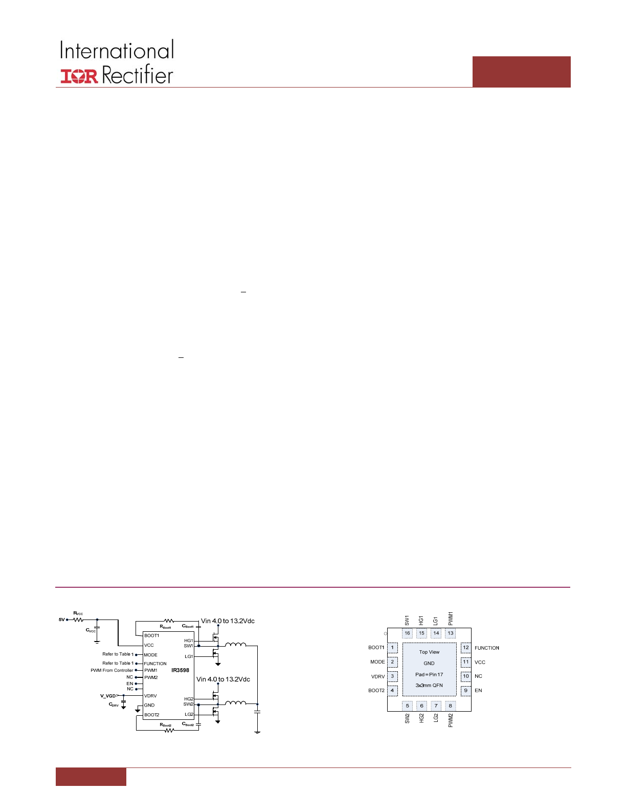
BASIC APPLICATION
Figure 1: IR3598 Typical DOUBLER Mode
Application Circuit
DESCRIPTION
The IR3598 is a high‐efficiency dual driver capable of switching
a pair of high and low side N‐channel MOSFETs in synchronous
buck converters and is optimized for use with IR’s Digital PWM
controllers to provide a total voltage regulator solution for today’s
advanced computing applications. In a space saving 16‐pin QFN
package, the IR3598 can significantly improve density in high
phase count voltage regulators saving over 50% board space
versus conventional drivers.
The IR3598 can be configured as two independent drivers in DUAL
mode with individual PWM signals, or as an interleaved DOUBLER
driver where one PWM signal is internally split to drive the two
pairs of MOSFETs 180° out of phase. The inter‐leaving action is
optimized internally to manage the tri‐state action of multiple
phases during transients, low current single phase operation, and
PS2 operation (see Figs. 8 and 9.) The DOUBLER mode can double
the effective maximum phase count from the controller, enabling
a well‐controlled, high phase count voltage regulator.
The IR3598 has a proprietary circuit which maintains the MOSFET
drive strength throughout the 4.0V to 13.2V drive voltage range
thus insuring fast switching even with 5V standby drive operation
during system sleep modes. The integrated boot diodes reduce
external component count. The IR3598 also features an adaptive
non‐overlap control for shoot‐through protection.
The IR3598 PWM inputs are compatible with IR’s fast Active
Tri‐Level (ATL) PWM signals as well as 3.3V and 5V Tri‐State
PWM signals.
APPLICATIONS
Desktop CPU and GPU solutions
Performance overclocking CPU and GPU VR solutions
Optimized for Sleep state S3 systems using +5VSB
PIN DIAGRAM
Figure 2: IR3598 Package Top View
Dual/Doubler Interleaved MOSFET Driver
October 25, 2013 | FINAL | V1.12
2
IR3598
ORDERING INFORMATION
IR3598
Package
Tape & Reel Qty
Part Number
QFN
3000
IR3598MTRPBF
QFN
100
IR3598MPBF
PBF – Lead Free
TR – Tape and Reel
M – QFN Package
Dual/Doubler Interleaved MOSFET Driver
October 25, 2013 | FINAL | V1.12
3
IR3598
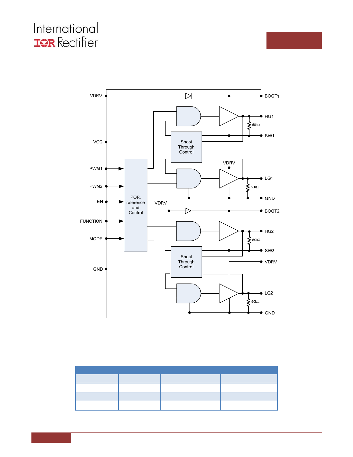
FUNCTIONAL BLOCK DIAGRAM
Figure 3: IR3598 Simplified Functional Block Diagram
T
ABLE
1:
M
ODE
C
ONFIGURATION
T
ABLE
Function
Mode
PWM Mode
Phase Mode
0
1
IR ATL
Dual
1
1
IR ATL
Doubler
0
0
Tri‐State
Dual
1
0
Tri‐State
Doubler
Dual/Doubler Interleaved MOSFET Driver
October 25, 2013 | FINAL | V1.12
4
IR3598
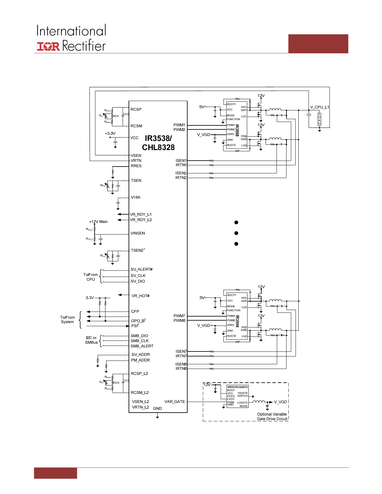
TYPICAL APPLICATIONS
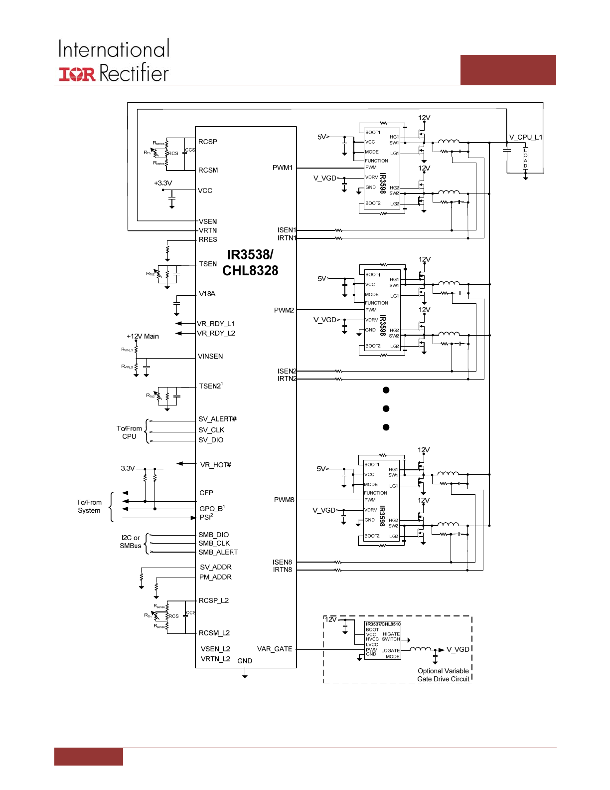
Figure 4: 8‐Phase CPU VR solution using IR3598 MOSFET drivers in DUAL mode & IR3538/CHL8328 Controller
with the IR3537/CHL8510 as a VGD Driver
Dual/Doubler Interleaved MOSFET Driver
October 25, 2013 | FINAL | V1.12
5
IR3598
Figure 5: 16‐Phase VR solution using IR3598 MOSFET drivers in DOUBLER mode & IR3538/CHL8328 Controller
with the IR3537/CHL8510 as a VGD
Dual/Doubler Interleaved MOSFET Driver
October 25, 2013 | FINAL | V1.12
6
IR3598
PIN DESCRIPTIONS
PIN #
PIN NAME
PIN DESCRIPTION
1
BOOT1
Floating bootstrap supply pin for the upper gate drive HG1. Connect the bootstrap capacitor between this pin
and the SW1 pin. The bootstrap capacitor provides the charge to turn on the upper MOSFET. See the Internal
Bootstrap Device section under DESCRIPTION for guidance in choosing the capacitor value.
2
MODE
The MODE pin is an input signal used to set the PWM MODE (Tri‐State or IR ATL) of the drivers.
The MODE pin levels are controlled by connecting the MODE pin to Ground or connecting to VCC. Refer to the
configuration instructions in Table 1 to program the mode pin. Do not let this pin float. The mode pin must be
directly connected to ground when this is the connection. Do not connect through a resistor when connecting
to ground. The mode pin is low when the pin voltage is below 0.8Vdc and high when the pin voltage is above
2Vdc.
3
VDRV
Connect this pin to a separate supply voltage between 4.0V and 13.2V to vary the drive voltage
on both the high side and low side MOSFET’s. Place a high quality low ESR ceramic capacitor from this pin to
GND. Note that on the high side MOSFET’s, the gate drive voltage will be VDRV less the boot strap diode voltage
drop.
4
BOOT2
Floating bootstrap supply pin for the upper gate drive HG2. Connect the bootstrap capacitor between this pin
and the SW2 pin. The bootstrap capacitor provides the charge to turn on the upper MOSFET. See the Internal
Bootstrap Device section under DESCRIPTION for guidance in choosing the capacitor value.
5
SW2
Connect this pin to the SOURCE of the upper MOSFET and the DRAIN of the lower MOSFET of the second power
stage, driven by HG2 and LG2. This pin provides a return path for the upper gate drive.
6
HG2
Upper gate drive output of Driver 2. Connect to gate of high‐side power N‐Channel MOSFET of the second
power stage.
7
LG2
Lower gate drive output of Driver 2. Connect to gate of the low‐side power N‐Channel MOSFET
of the second power stage.
8
PWM2
The PWM2 signal is the control input for the second driver from either an IR ATL compatible source or an
industry standard Tri‐State source. Connect this pin to the PWM output of the controller.
As a DUAL driver, PWM2 controls the behavior of Gate Driver 2 (HG2, LG2). In DOUBLER mode this pin is not
used and must be left open.
9
EN
The chip will be enabled with the EN pin left open, or pulled high to VCC. The enable is low when the pin
voltage is below 0.8Vdc and high when the pin voltage is above 2Vdc.
10
NC
This pin must be left open.
11
VCC
Connect this pin to a +5V bias supply. Place a high quality low ESR 0.1uF ceramic capacitor from this pin to the
IR3598 GND.
12
FUNCTION
The FUNCTION pin controls the Phase Mode (Dual or Doubler Modes). The FUNCTION pin levels are controlled
by connecting the FUNCTION pin to Ground or VCC. Refer to the configuration instructions in Table 1 to
program the FUNCTION pin. At power up, the function pin selection is latched into the IR3598, and therefore
cannot be changed after initial power up. The function pin is low when the pin voltage is below 1 Vdc and high
when the pin voltage is above 4.2Vdc.
13
PWM1
The PWM1 signal is the control input for the first driver from either an IR ATL compatible source
or an industry standard Tri‐State source. Connect this pin to the PWM output of the controller.
As a DUAL driver, PWM1 controls the behavior of Gate Driver 1 (HG1, LG1). In DOUBLER mode
PWM1 controls the behavior of Gate Drive 1 (HG1, LG1) and Gate Drive 2 (HG2, LG2).
14
LG1
Lower gate drive output of Driver 1. Connect to gate of the low‐side power N‐Channel MOSFET
of the first power stage.
15
HG1
Upper gate drive output of Driver 1. Connect to gate of high‐side power N‐Channel MOSFET
of the first power stage.
16
SW1
Connect this pin to the SOURCE of the upper MOSFET and the DRAIN of the lower MOSFET of the first power
stage. This pin provides a return path for the upper gate drive.
(PAD) 17
GND
Bias and reference ground. All signals are referenced to this node. It is also the power ground return of the
driver.
Dual/Doubler Interleaved MOSFET Driver
October 25, 2013 | FINAL | V1.12
7
IR3598
ABSOLUTE MAXIMUM RATINGS
Stresses beyond those listed under “Absolute Maximum Ratings” may cause permanent damage to the device. These are
stress ratings only and functional operation of the device at these or any other conditions beyond those indicated in the
operational sections of the specifications are not implied.
Voltage Regulator Vin
4.0 to 13.2Vdc
VCC
‐0.3V to +7.0V
VDRV
‐0.3V to +15.0V
PWM1, PWM2, EN, MODE, FUNCTION
‐0.3V to VCC +0.3V
BOOTx‐GND, BOOTx – SWx
‐0.3V to +35V, ‐0.3V to +15.0V
LG1, LG2
DC ‐0.3V to VDRV + 0.3V, <200ns: ‐5V to VDRV + 0.3V
HG1, HG2
SWx – 0.3V to VBOOT + 0.3V, <20ns: SWx – 5V to VBOOT + 0.3V
SW1, SW2
‐0.3V to +35V, <200nS, ‐8V
ESD
750V HBM
Thermal Information
Thermal Resistance (ΘJC)
3°C/W
Thermal Resistance (ΘJA)
1
45°C/W
Maximum Junction Temperature
150°C
Maximum Storage Temperature Range
‐65°C to 150°C
Maximum Lead Temperature (Soldering 10s)
300°C
Note 1: θJA is measured with the component mounted on a high effective thermal conductivity test board in free air.
Dual/Doubler Interleaved MOSFET Driver
October 25, 2013 | FINAL | V1.12
8
IR3598
ELECTRICAL SPECIFICATIONS
RECOMMENDED OPERATING CONDITIONS FOR RELIABLE OPERATION WITH MARGIN
Recommended Voltage Regulator Vin Range
4.5 to 13.2Vdc
Recommended Operating Ambient Temperature Range
0°C to 85°C
Maximum Operating Junction Temperature
125°C
VCC Supply Voltage Range
+5V ± 10%
VDRV
4.0V to 13.2V
ELECTRICAL CHARACTERISTICS
Unless otherwise specified, these specifications were tested at +25°C. VCC = VDRV = 5.0V.
PARAMETER
SYMBOL
CONDITIONS
MIN
TYP
MAX
UNIT
Supply
Supply Bias Current Shutdown – Dual
Mode
I
VCC +
I
VDRV
ENABLE LOW
1.8
2.1
2.7
mA
Supply Bias Current Idle – Dual Mode
I
VCC +
I
VDRV
Tri‐stated Gate Driver
2.6
3.3
4.0
mA
Supply Bias Current Idle – Doubler Mode
I
VCC +
I
VDRV
Tri‐stated Gate Driver
2.1
2.9
3.6
mA
Supply Bias Current ―Note 1
I
VCC +
I
VDRV
f
PWM
= 300kHz, no load
‐
4.5
‐
mA
VCC Rising Threshold for POR
3.55
3.80
3.98
V
VCC Falling Threshold for POR
3.20
3.50
3.80
V
Vdrive Rising Threshold for POR
3.55
3.80
3.98
V
Vdrive Falling Threshold for POR
2.50
2.75
3.00
V
PWM Input IR ATL Mode
PWM Input Pull‐Up Voltage
VPWM_pull up
PWM Input Floating
‐
4.0
‐
V
PWM Input High Threshold
V
IH(C_PWM)
0.9
1.15
1.3
V
PWM Input Low Threshold
V
IL(C_PWM)
0.7
0.95
1.1
V
PWM Tri‐level High Threshold
V
TL(C_PWM)
2.4
2.65
2.9
V
PWM Tri‐level Low Threshold
V
TH(C_PWM)
2.2
2.5
2.7
V
PWM Input Current Low
I
C_PWM
V
PWM
= 0V
0.7
1.0
1.4
mA
PWM Input Current High
V
PWM
= 1.8V
0.7
1.0
1.4
mA
PWM Input Current Tri‐state
V
PWM
= 3.3V
60
125
190
uA
PWM Input Tri‐State Mode (+3.3V or +5V signal level)
PWM Input Rising Threshold, Note 1
V
IH(C_PWM)
‐
1.65
‐
V
PWM Input Falling Threshold, Note 1
V
IL(C_PWM)
‐
1.3
‐
V
Tri‐State LO_GATE Threshold
0.7
0.95
1.1
V
Tri‐State LO_GATE Hysteresis
100
200
300
mV
Tri‐State HI_GATE Threshold
2.4
2.65
2.9
V
Dual/Doubler Interleaved MOSFET Driver
October 25, 2013 | FINAL | V1.12
9
IR3598
PARAMETER
SYMBOL
CONDITIONS
MIN
TYP
MAX
UNIT
Tri‐State HI_GATE Hysteresis
100
200
300
mV
Tri‐State Hold Off Time, Note 1
‐
80
‐
ns
PWM Input Pull‐Up Voltage
VPWM_pull up
PWM Input Floating
1.3
1.55
1.9
V
PWM Input Resistance, Note 1
RPWM
PWM Input Floating
‐
3.75
‐
kΩ
Minimum Recognized PWM Pulse Width,
Note 1
ATL (IR) and Tri‐State Modes
‐
40
‐
nSec
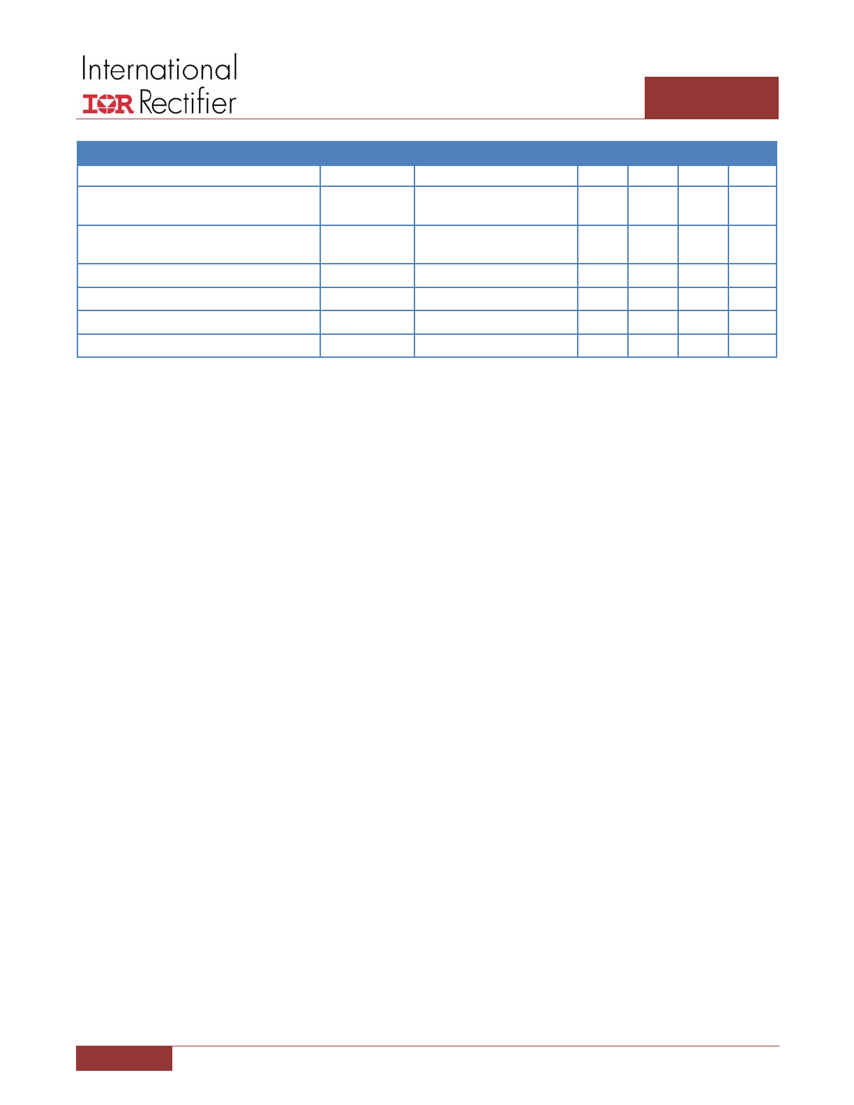
High Side Gate Drivers
Transi on Time ― Rise, Note1
t
R(HS)
3nF Load, VDRV = 5‐12V
‐
15
‐
ns
Transi on Time ― Fall, Note1
t
F(HS)
3nF Load, VDRV = 12V
‐
12
‐
ns
Transi on Time ― Fall, Note1
t
F(HS)
3nF Load, VDRV = 5V
‐
17
‐
ns
Propaga on Delay ― Turn‐on all modes,
Note 1
t
PDH(HS)
3nF Load, VDRV = 5‐12V
‐
23
‐
ns
Propaga on Delay ― Turn‐off Dual, Note
1
t
PDL(HS)
3nF Load, VDRV = 5‐12V
‐
17
‐
ns
Propaga on Delay ― Turn‐off Doubler,
Note 1
t
PDL(HS)
3nF Load, VDRV = 5‐12V
‐
24
‐
ns
Propaga on Delay ― Exit Tri‐State Dual,
Note 1
t
PDTS(HS_en)
3nF Load
‐
40
‐
ns
Propaga on Delay ― Exit Tri‐State
Doubler, Note 1
t
PDTS(HS_en)
3nF Load
‐
40
‐
ns
Propaga on Delay ― Enter Tri‐State
Dual, Note 1
t
PDTS(HS_dis)
3nF Load
‐
19
‐
ns
Propaga on Delay ― Enter Tri‐State
Doubler, Note 1
t
PDTS(HS_dis)
3nF Load
‐
19
‐
ns
Output Impedance Source, Note 1
R
HS_SOURCE
VDRV = 12V, 100mA
‐
1.1
‐
Ω
Output Impedance Source, Note 1
R
HS_SOURCE
VDRV = 5V, 100mA
‐
1.4
‐
Ω
Output Impedance ― Sinking, Note 1
R
HS_SINK
VDRV = 12V, 100mA
‐
0.60
‐
Ω
Output Impedance ― Sinking
R
HS_SINK
VDRV = 5V, 100mA
0.70
0.90
1.20
Ω
Low Side Gate Drivers
Transi on Time ― Rise, Note 1
t
R(LS)
3nF Load, VDRV = 5‐12V
‐
14
‐
ns
Transi on Time ― Fall, Note 1
t
F(LS)
3nF Load, VDRV = 12V
‐
7
‐
ns
Transi on Time ― Fall, Note 1
t
F(LS)
3nF Load, VDRV = 5V
‐
8.5
‐
ns
Propaga on Delay ― Turn‐on all modes,
Note 1
t
PDH(LS)
3nF Load, VDRV = 5‐12V
‐
20
‐
ns
Propaga on Delay ― Turn‐off Dual, Note
1
t
PDL(LS)
3nF Load, VDRV = 5‐12V
‐
18
‐
ns
Propaga on Delay ― Turn‐off Doubler,
Note 1
t
PDL(LS)
3nF Load, VDRV = 5‐12V
‐
24
‐
ns
Propaga on Delay ― Exit Tri‐State Dual,
Note 1
t
PDTS(LS_en)
3nF Load
‐
24
‐
ns
Propaga on Delay ― Exit Tri‐State
t
PDTS(LS_en)
3nF Load
‐
30
‐
ns
Dual/Doubler Interleaved MOSFET Driver
October 25, 2013 | FINAL | V1.12
10
IR3598
PARAMETER
SYMBOL
CONDITIONS
MIN
TYP
MAX
UNIT
Doubler, Note 1
Propaga on Delay ― Enter Tri‐State
Dual, Note 1
t
PDTS(LS_dis)
3nF Load
‐
15
‐
ns
Propaga on Delay ― Enter Tri‐State,
Doubler, Note 1
t
PDTS(LS_dis)
3nF Load
‐
23
‐
ns
Output Impedance Source, Note 1
R
LS_SOURCE
VDRV = 12V, 100mA
‐
0.85
‐
Ω
Output Impedance Source, Note 1
R
LS_SOURCE
VDRV = 5V, 100mA
‐
1.0
‐
Ω
Output Impedance ― Sinking, Note 1
R
LS_SINK
VDRV = 12V, 100mA
‐
0.38
‐
Ω
Output Impedance ― Sinking
R
LS_SINK
VDRV = 5V, 100mA
0.45
0.55
0.75
Ω
Note 1: Guaranteed by design but not tested in production.