
www.irf.com
| © 2014 International Rectifier
January 9, 2015 | V1.2
1
IR3537
CHL8510
12V High Performance Gate Driver
FEATURES
Drives both high‐side and low‐side MOSFETs in a
synchronous buck configuration
Large drivers designed to drive 6nF server class FETs
o
Low‐side driver – 4A source / 6A sink
o
High‐side driver – 3A source / 4A sink
o
Transition times & propagation delays < 20ns
Independent variable gate drive voltage for both
high‐ and low‐side drivers from 4.5V to 13.2V
o
Improves efficiency
o
Compatible with IR controller VGD feature
Integrated bootstrap diode
o
Reduces external component count
Capable of high switching frequencies from 200kHz
up to 1MHz
Configurable PWM modes of operation
o
IR Active Tri‐Level (ATL), disables both MOSFETs
in 30ns with no hold‐off time
o
Generic Tri‐State PWM with hold‐off
Adaptive non‐overlap protection minimizes diode
conduction time
Input supply under voltage protection
Thermally enhanced 10‐pin DFN package
Lead free RoHS compliant package, MSL level 1
APPLICATIONS
Multiphase synchronous buck converter for
Server and desktop computers using Intel® and
AMD® VR solutions
High efficiency and compact VRM
High current DC/DC converters
BASIC APPLICATION
Figure 1: Basic Applications Circuit
DESCRIPTION
The IR3537/CHL8510 is a high efficiency gate driver which
can switch both high‐side and low‐side N‐channel external
MOSFETs in a synchronous buck converter. It is intended
for use with International Rectifier’s Digital PWM
controllers to provide a total voltage regulator (VR)
solution for today’s advanced computing applications.
The IR3537/CHL8510 low‐side driver is capable of rapidly
switching large MOSFETs with low R
DS(on)
and large input
capacitance used in high efficiency designs.
The IR3537/CHL8510 features individual control of
both the high‐and low‐side gate drive voltages from
4.5V to 13.2V. This enables the optimization of switching
and conduction losses in the external MOSFETs. When
used with IR’s proprietary Variable Gate Drive (VGD)
technology, a significant improvement in efficiency is
observed across the entire load range.
The IR3537/CHL8510 can be configured to drive both the
high‐ and low‐side switches from the unique IR fast Active
Tri‐Level (ATL) PWM signal or a generic tri‐state PWM
mode. The IR ATL mode allows the controller to disable
the high‐ and low‐side FETs in less than 30ns without the
need for a dedicated disable pin. This improves VR
transient performance, especially during load release.
The integrated bootstrap diode reduces external
component count. The IR3537/CHL8510 also features
an adaptive non‐overlap control for shoot‐through
protection. This prevents cross conduction of both high‐
side and low‐side MOSFETs and minimizes body diode
conduction time to provide the best in class efficiency.
PIN DIAGRAM
Figure 2: IR3537/CHL8510 Package Top View
www.irf.com
| © 2014 International Rectifier
January 9, 2015 | V1.2
2
IR3537
CHL8510
12V High Performance Gate Driver
ORDERING INFORMATION
IR3537
M
CHL8510
Package
Tape & Reel Qty
Part Number
DFN
3000
IR3537MTRPBF
DFN
750
IR3537MTR1PBF
Package
Tape & Reel Qty
Part Number
DFN
3000
CHL8510CRT
PBF – Lead Free
TR – Tape and Reel
Package Type (DFN)
T – Tape and Reel
R – Package Type (DFN)
C – Operating Temperature
(Commercial Standard)
www.irf.com
| © 2014 International Rectifier
January 9, 2015 | V1.2
3
IR3537
CHL8510
12V High Performance Gate Driver
FUNCTIONAL BLOCK DIAGRAM
Figure 3: IR3537/CHL8510 Functional Block Diagram
PIN DESCRIPTIONS
PIN #
PIN NAME
PIN DESCRIPTION
1
BOOT
Floating bootstrap supply pin for the upper gate drive. Connect a bootstrap capacitor between
this pin and the SWITCH pin. The bootstrap capacitor provides the charge to turn on the upper
MOSFET. See the Internal Bootstrap Device section under DESCRIPTION for guidance in choosing
the capacitor value.
2
HVCC
Connect this pin to VCC (+12V) or to a separate supply between 4.5V and 13.2V to provide a lower
gate drive voltage on the high‐side MOSFETs. It is connected to the anode of the internal bootstrap
diode. Place a high‐quality low ESR ceramic capacitor from this pin to GND.
3
PWM
The PWM signal is the control input for the driver from a 1.8V or 3.3V PWM signal. The PWM signal
can enter three distinct states during operation; see the three‐state PWM Input section under
DESCRIPTION for further details. Connect this pin to the PWM output of the controller.
4
VCC
Connect this pin to a +12V bias supply. Place a high quality low ESR ceramic capacitor from this
pin to GND.
5
LVCC
Connect this pin to VCC (+12V) or a separate supply voltage between 4.5V and 13.2V to vary the drive
voltage on the low‐side MOSFETs. Place a high‐quality low ESR ceramic capacitor from this pin to GND.
This pin must always be ≤ VCC+0.7Vdc.
6
LO_GATE
Lower gate drive output. Connect to gate of the low‐side power N‐Channel MOSFET.
7
GND
Bias and reference ground. All signals are referenced to this node. It is also the power ground return
of the driver.
8
MODE
This pin allows selection of the PWM signal voltage for 1.8V or 3.3V normal operation. Floating this pin
configures the driver for IR Active Tri‐Level (ATL) using 1.8V PWM, and connecting this pin to ground
configures the driver for generic active tri‐state operation using 3.3V PWM.
9
SWITCH
Connect this pin to the SOURCE of the upper MOSFET and the DRAIN of the lower MOSFET. This pin
provides a return path for the upper gate drive.
10
HI_GATE
Upper gate drive output. Connect to gate of high‐side power N‐Channel MOSFET.
PAD (11)
GND
Bias and reference ground. All signals are referenced to this node. It is also the power ground return
of the driver.
POR,
reference
and
Control
Shoot
Through
Control
LVCC
LO_GATE
HI_GATE
GND
SWITCH
PWM
VCC
BOOT
MODE
HVCC
www.irf.com
| © 2014 International Rectifier
January 9, 2015 | V1.2
4
IR3537
CHL8510
12V High Performance Gate Driver
TYPICAL APPLICATIONS BLOCK DIAGRAMS
Figure 4: 6‐Phase Voltage Regulator using IR3537/CHL8510 MOSFET drivers & CHL8316 Controller
www.irf.com
| © 2014 International Rectifier
January 9, 2015 | V1.2
5
IR3537
CHL8510
12V High Performance Gate Driver
ABSOLUTE MAXIMUM RATINGS
BOOT
+35.0V reference to GND,
+15V reference to SWITCH
PWM
+7.0V
VCC, HVCC
+15.0V
LVCC
VCC+0.7Vdc to a maximum of +15.0V
LO_GATE
DC: ‐0.3V to <0.3V above Vcc,
<200ns: ‐2V to <0.3V above Vcc
GND
0V+/‐ 0V
SWITCH
DC: ‐0.3V to +15V, <20nS: 25V, <5nS: ‐10V,
<20 ns: ‐4Vdc and <200 ns: ‐2Vdc
HI_GATE
DC: SWITCH – 0.3V to 0.3V above VBOOT,
<200ns: SWITCH – 2V to 0.3V above VBOOT
MODE
‐0.3V to +15.0V
ESD – Charged Device Model JESD22‐C101‐C
Passes +/‐1000V
THERMAL INFORMATION
Thermal Resistance (θ
JC
)
3°C/W
Thermal Resistance (θ
JA
)
1
45°C/W
Maximum Operating Junction Temperature
150°C
Maximum Storage Temperature Range
‐65°C to 150°C
Maximum Lead Temperature (Soldering 10s)
300°C
Note 1: θ
JA
is measured with the component mounted on a high effective thermal conductivity test board in free air.
Stresses beyond those listed under “Absolute Maximum Ratings” may cause permanent damage to the device. These are stress ratings
only and functional operation of the device at these or any other conditions beyond those indicated in the operational sections of the
specifications are not implied.
www.irf.com
| © 2014 International Rectifier
January 9, 2015 | V1.2
6
IR3537
CHL8510
12V High Performance Gate Driver
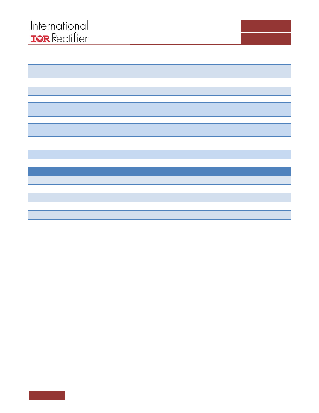
ELECTRICAL SPECIFICATIONS
The electrical characteristics involve the spread of values guaranteed within the recommended operating conditions.
Typical values represent the median values, which are related to 25°C.
RECOMMENDED OPERATING CONDITIONS FOR RELIABLE OPERATION WITH MARGIN
Recommended Operating Ambient Temperature
0°C to 85°C
Recommended Operating Junction Temperature
125°C
Recommended Supply Voltage Range
+12V ± 10%
Recommended LVCC & HVCC Range
(note LVCC must be ≤Vcc +0.7Vdc)
+4.5V to 13.2V
ELECTRICAL CHARACTERISTICS
PARAMETER
SYMBOL
CONDITIONS
MIN
TYP
MAX
UNIT
Supply
Supply Bias Current
I
VCC
f
PWM
= 300kHz,
V
VCC
= 12V, no load
‐
7.0
‐
mA
Quiescent Bias Current
I
DD
‐
5.0
‐
mA
VCC Rising Threshold for POR
‐
8.6
‐
V
VCC Falling Threshold for POR
‐
7.1
‐
V
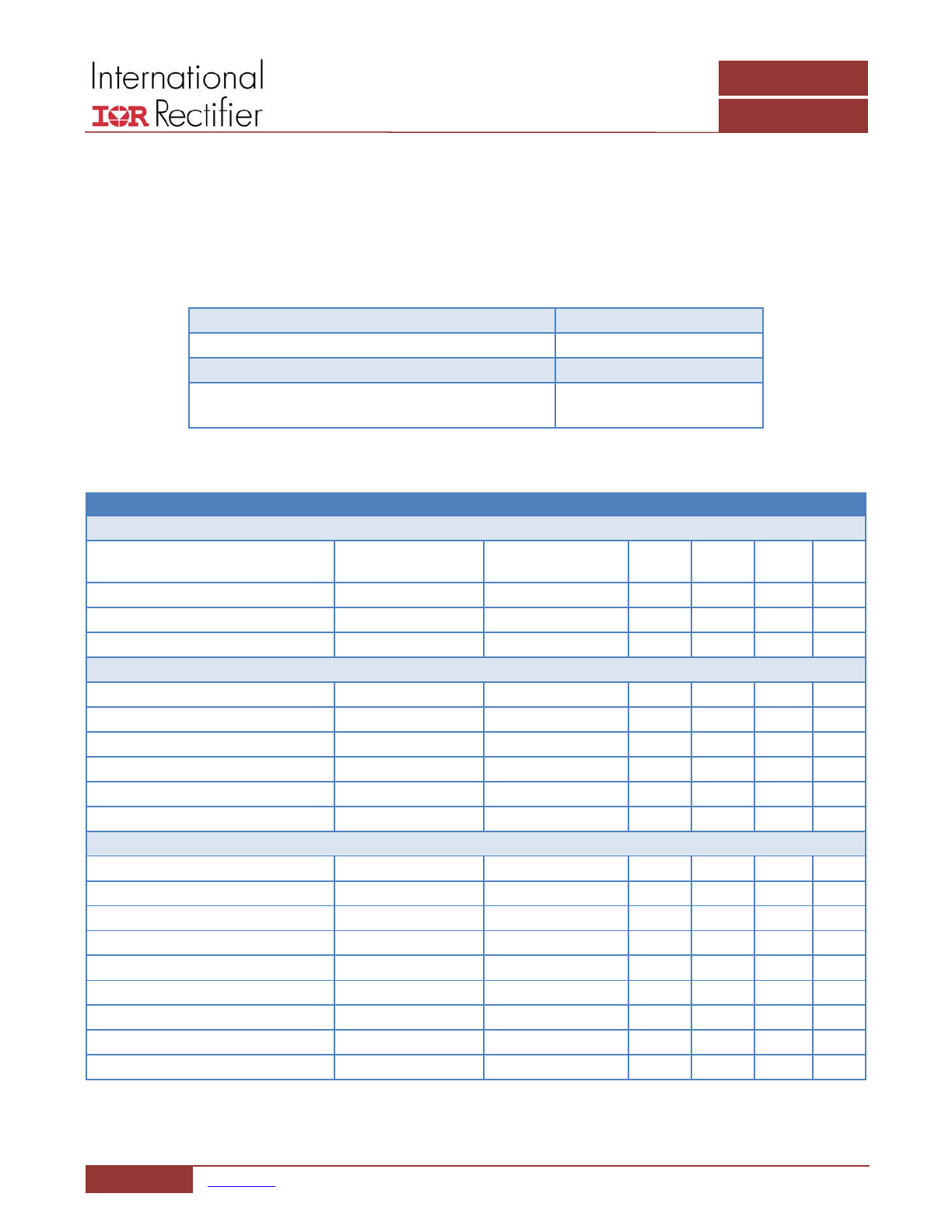
PWM Input Active Tri‐Level Mode (See Figure 5)
PWM Input High Threshold
V
IH(C_PWM)
VCC = 12V
‐
1.0
‐
V
PWM Input Low Threshold
V
IL(C_PWM)
VCC = 12V
‐
0.8
‐
V
PWM Tri‐Level Hi Threshold
V
TL(C_PWM)
VCC = 12V
‐
2.65
‐
V
PWM Tri‐Level Low Threshold
V
TH(C_PWM)
VCC = 12V
‐
2.55
‐
V
PWM Input Current Low
I
C_PWM
V
pwm
= 0V
‐
‐0.88
‐
mA
PWM Input Current High
V
pwm
= 3.3V
‐
‐10
‐
µA
PWM Input Tri‐State Mode (See Figure 6)
PWM Input Rising Threshold
V
IH(C_PWM)
VCC = 12V
‐
1.65
‐
V
PWM Input Falling Threshold
V
IL(C_PWM)
VCC = 12V
‐
1.3
‐
V
Tri‐State LO_GATE Threshold
‐
0.85
‐
V
Tri‐State LO_GATE Hysteresis
‐
200
‐
mV
Tri‐State HI_GATE Threshold
‐
2.55
‐
V
Tri‐State HI_GATE Hysteresis
‐
200
‐
mV
Tri‐State Hold‐off Time, Note 1
‐
80
‐
ns
PWM Input Pull‐up Voltage
V
PWM_pullup
PWM input floating
‐
1.65
‐
V
PWM Input Resistance
R
PWM
PWM input floating
‐
3.75
‐
kΩ

www.irf.com
| © 2014 International Rectifier
January 9, 2015 | V1.2
7
IR3537
CHL8510
12V High Performance Gate Driver
High‐Side Gate Driver
Transition Time, Rising, Note 1
t
R(HS)
6nF Load, V
VCC
= 12V,
10% ‐ 90%
‐
21
‐
ns
Transition Time, Falling, Note 1
t
F(HS)
6nF Load, V
VCC
= 12V,
10% ‐ 90%
‐
18
‐
ns
Transition Time, Rising, Note 1
t
R(HS)
3nF Load, V
VCC
= 12V,
10% ‐ 90%
‐
15
‐
ns
Transition Time, Falling, Note 1
t
F(HS)
3nF Load, V
VCC
= 12V,
10% ‐ 90%
‐
12
‐
ns
Propagation Delay, Turn‐On, Note 1
t
PDH(HS)
6nF Load, V
VCC
= 12V,
Adaptive
‐
16
‐
ns
Propagation Delay, Turn‐Off, Note 1
t
PDL(LS)
6nF Load, V
VCC
= 12V
‐
17
‐
ns
Propagation Delay , Exit Tri‐State,
Note 1
t
PDTS(HS_en)
6nF Load, V
VCC
= 12V
‐
29
‐
ns
Propagation Delay, Enter Tri‐State,
Note 1
t
PDTS(HS_dis)
6nF Load, V
VCC
= 12V
‐
16
‐
ns
Source Current, Note 1
I
HS_SOURCE
6nF Load, V
VCC
= 12V
‐
3.0
‐
A
Output Impedance, Sourcing
R
HS_SOURCE
Sink Current at
100mA
‐
1.6
‐
Ω
Sink Current, Note 1
I
HS_SINK
6nF Load, V
VCC
= 12V
‐
4.0
‐
A
Output Impedance, Sinking
R
HS_SINK
Sink Current at
100mA
‐
0.6
‐
Ω
Low‐Side Gate Driver
Transition Time, Rising, Note 1
t
F(LS)
6nF Load, V
VCC
= 12V,
10% ‐ 90%
‐
18
‐
ns
Transition Time, Falling, Note 1
t
R(LS)
6nF Load, V
VCC
= 12V,
10% ‐ 90%
‐
13
‐
ns
Transition Time, Rising, Note 1
t
F(LS)
3nF Load, V
VCC
= 12V,
10% ‐ 90%
‐
13
‐
ns
Transition Time, Falling, Note 1
t
R(LS)
3nF Load, V
VCC
= 12V,
10% ‐ 90%
‐
9
‐
ns
Propagation Delay, Turn‐On, Note 1
t
PDH(LS)
6nF Load, V
VCC
= 12V,
Adaptive
‐
17
‐
ns
Propagation Delay, Turn‐Off, Note 1
t
PDL(LS)
6nF Load, V
VCC
= 12V
‐
13
‐
ns
Propagation Delay, Exit Tri‐State,
Note 1
t
PDTS(LS_en)
6nF Load, V
VCC
= 12V
‐
26
‐
ns
Propagation Delay, Enter Tri‐State,
Note 1
t
PDTS(LS_dis)
6nF Load, V
VCC
= 12V
‐
14
‐
ns
Source Current, Note 1
I
LS_SOURCE
6nF Load, V
VCC
= 12V
‐
4.0
‐
A
Output Impedance, Sourcing
R
LS_SOURCE
Sink Current at
100mA
‐
1.5
‐
Ω
Sink Current, Note 1
I
LS_SINK
6nF Load, V
VCC
= 12V
‐
6
‐
A
Output Impedance, Sinking
R
LS_SINK
Sink Current at
100mA
‐
0.4
‐
Ω
Note 1: Guaranteed by design but not tested in production.
www.irf.com
| © 2014 International Rectifier
January 9, 2015 | V1.2
8
IR3537
CHL8510
12V High Performance Gate Driver
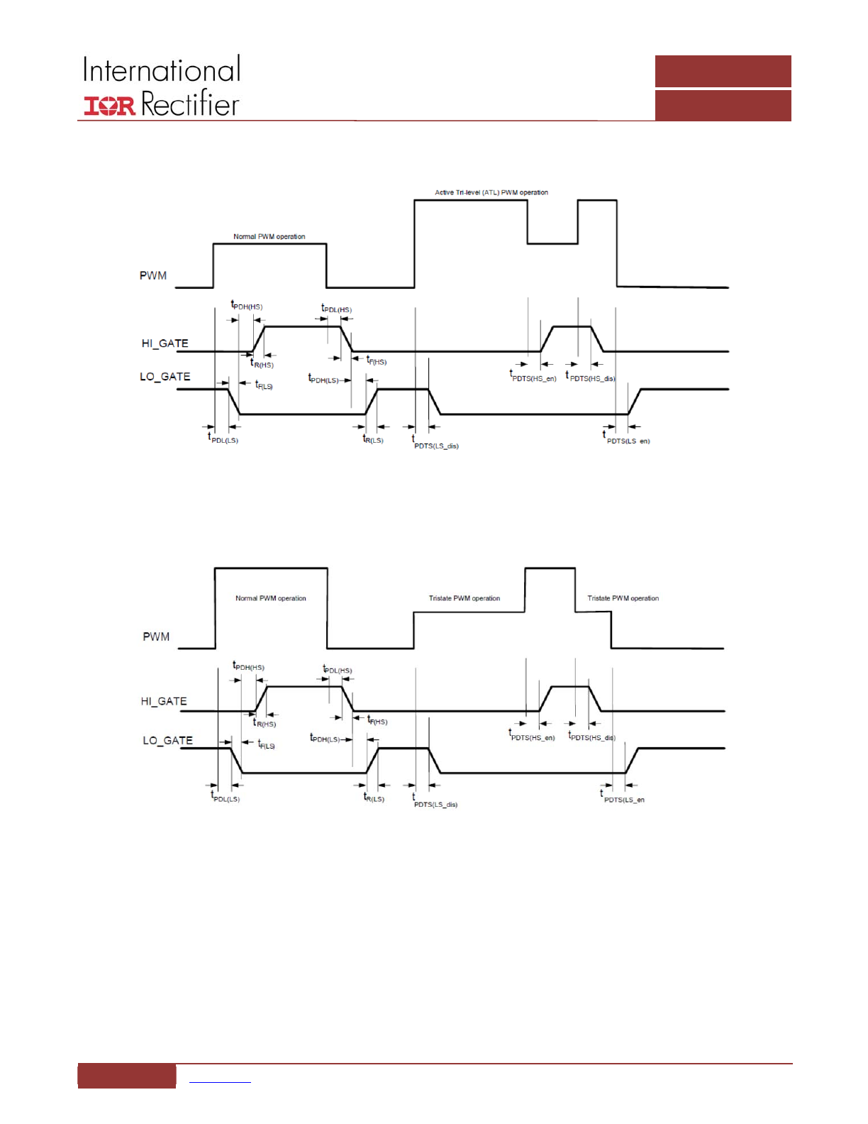
TIMING DIAGRAMS
Figure 5: Active Tri‐Level Mode PWM, HI_GATE and LO_GATE Signals
Figure 6: Tri‐State Mode PWM, HI_GATE and LO_GATE Signals

www.irf.com
| © 2014 International Rectifier
January 9, 2015 | V1.2
9
IR3537
CHL8510
12V High Performance Gate Driver
GENERAL DESCRIPTION
The IR3537/CHL8510 is a high efficiency, fast MOSFET
driver with large source and sink current capability. It can
reliably drive the external high‐ and low‐side N‐channel
MOSFETs with large input capacitance at switching
frequencies up to 1MHz. The proprietary IR Active Tri‐Level
(ATL) feature allows complete control over enable and
disable of both MOSFETs using the PWM input signal from
the controller. The driver is also compatible with a generic
tri‐state PWM signal. The Active Tri‐Level or tri‐state is
selectable by the MODE pin.
During normal operation the PWM transitions between
low and high voltage levels to drive the low‐ and high‐side
MOSFETs. The PWM signal falling edge transition to a low
voltage threshold initiates the high‐side driver turn off
after a short propagation delay, t
PDL(HS)
. The dead time
control circuit monitors the HI_GATE and switch voltages
to ensure the high‐side MOSFET is turned off before the
LO_GATE voltage is allowed to rise to turn on the low‐side
MOSFET.
The PWM rising edge transition through the high‐side turn‐
on threshold initiates the turn off of the low‐side MOSFET
after a small propagation delay, t
PDL(LS).
The adaptive dead
time circuit provides the appropriate dead time by
determining if the falling LO_GATE voltage threshold has
been crossed before allowing the HI_GATE voltage to rise
and turn on the high‐side MOSFET, t
PDH(HS)
.
THEORY OF OPERATION
POWER‐ON RESET (POR)
The IR3537/CHL8510 incorporates a power‐on reset
feature. This ensures that both the high‐ and low‐side
output drivers are made active only after the device supply
voltage has exceeded a certain minimum operating
threshold. The Vcc supply is monitored and both the
drivers are set to the low state, holding both external
MOSFETs off. Once Vcc crosses the rising POR threshold,
the IR3537/CHL8510 is reset and the outputs are held in
the low state until a transition from tri‐state to active
operation is detected at the PWM input. During normal
operation the drivers continue to remain active until the
Vcc falls below the falling POR threshold.
These POR voltage threshold levels allow seamless
functionality with International Rectifier’s digital
controllers, such that the drivers are always active before
the controller starts to provide the PWM signal and are
inactive only after the controller shuts down.
INTEGRATED BOOTSTRAP DIODE
The IR3537/CHL8510 features an integrated bootstrap
diode to reduce external component count. This enables
the IR3537/CHL8510 to be used effectively in cost and
space sensitive designs.
The bootstrap circuit is used to establish the gate voltage
for the high‐side driver. It consists of a diode and capacitor
connected between the SWITCH and BOOT pins of the
device. Integrating the diode within the IR3537/CHL8510,
results in the need for an external boot capacitor only.
The bootstrap capacitor is charged through the diode and
injects this charge into the high‐side MOSFET input
capacitance when PWM signal goes high.
PWM MODE SELECTION
The IR3537/CHL8510 features a MODE pin which
allows operation with different PWM signal levels.
The IR3537/CHL8510 is capable of driving external
MOSFETs based on one of two different tri‐level PWM
input signals from a controller.
Floating the MODE pin enables the IR3537/CHL8510 to
switch external FETs based on the IR Active Tri‐Level mode.
In ATL mode, the PWM voltage level is from 0V to 1.8V for
low to high transitions. A PWM voltage level greater than
the tri‐state HI_GATE threshold disables switching of both
MOSFETs. Grounding the MODE pin enables the
www.irf.com
| © 2014 International Rectifier
January 9, 2015 | V1.2
10
IR3537
CHL8510
12V High Performance Gate Driver
IR3537/CHL8510 to switch FETs based on a generic tri‐
state signaling with the PWM signal from 0V to 3.3V for
low to high transitions. A PWM voltage level in the tri‐state
window between 1.23V and 1.82V for 80ns results in
disabling both external MOSFETs.
IR ACTIVE TRI‐LEVEL PWM INPUT SIGNAL
The IR3537/CHL8510 gate drivers are driven by a unique
tri‐level PWM control signal provided by the International
Rectifier’s digital PWM controllers. During normal
operation, the rising and falling edges of the PWM signal
transitions between 0V and 1.8V to switch the LO_GATE
and HI_GATE. To force both driver outputs low
simultaneously, the PWM signal crosses a tri‐state voltage
level higher than the tri‐state HI_GATE threshold. This
threshold based tri‐state results in a very fast disable with
only a small tri‐state propagation delay. MOSFET switching
resumes when the PWM signal falls below the tri‐state
threshold into the normal operating voltage range.
This fast tri‐state operation eliminates the need for the
PWM signal to dwell in the shutdown window, eliminating
any hold‐off time. In addition, the disable delay time is
not affected by the PWM trace routing capacitance.
A dedicated enable pin is not required which simplifies the
routing and layout in applications with a limited number
of board layers. It also provides switching free of shoot
through for PWM transition times of up to 20ns. The
IR3537/CHL8510 is therefore tolerant of stray capacitance
on the PWM signal lines.
The IR3537/CHL8510 provides a 0.88mA typical pull‐up
current to drive the PWM input to the tri‐state condition of
3.3V when the PWM controller output is in its high
impedance state. The 0.88mA typical current is designed
for driving worst case stray capacitances and transition the
IR3537/CHL8510 into the tri‐state condition rapidly to
avoid a prolonged period of conduction of the high‐ or low‐
side MOSFETs during faults. Once the PWM signal has been
pulled up, the current is disabled to reduce power
consumption.
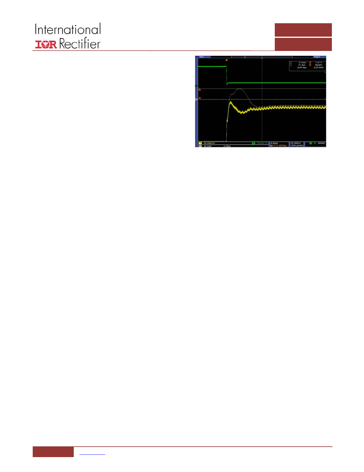
DIODE EMULATION DURING LOAD RELEASE
One advantage of ATL is the ability to quickly turn‐off all
low‐side MOSFETs during a load release event. This is
known as diode emulation since all the load current is
forced to flow momentarily through the body diodes of the
MOSFETs. This results in a much lower overshoot on the
output voltage as can be seen in Figure 7.
Figure 7: Output voltage overshoot reduction
with body‐braking
START UP
During initial startup, the IR3537/CHL8510 holds both
high‐ and low‐side drivers low even after POR threshold is
reached. This mode is maintained while the PWM signal is
pulled to the tri‐state threshold level greater than the
tri‐state HI_GATE threshold and until it transitions out of
tri‐state. It is this initial transition out of the tri‐state which
enables both drivers to switch based on the normal PWM
voltage levels.
This startup also ensures that any undetermined PWM
signal levels from a controller in pre‐POR state will not
result in high or low‐side MOSFET turn on until the
controller is out of its POR.
Note: The CHL8510/IR3537 driver requires that the LVCC
and VCC supply voltages be sequenced and operated
under all start‐up, operating, and shutdown conditions
such that Vcc is always greater than LVCC ‐0.7Vdc. Failure
to do this properly can cause catastrophic damage to the
CHL8510/IR3537 driver.
HIGH‐SIDE DRIVER
The high‐side driver drives an external floating N‐channel
MOSFET which can be switched at up to 1MHz. An external
bootstrap circuit referenced to the SWITCH node,
consisting of a boot diode and capacitor is used to bias the
external MOSFET gate. When the SWITCH node
is at ground, the boot capacitor is charged to the voltage
on the HVCC pin less the forward drop of the diode. This
stored charge is used to turn on the high‐side MOSFET
when the PWM signal goes high. Once the high‐side
MOSFET is turned on, the SWITCH voltage is raised to the
supply voltage, and the BOOT voltage is equal to the
I_out 105A to 10A
V_out without diode emulation
Overshoots ~25mV over 0A level
I_out 105A to 10A
V_out without diode emulation
Overshoots ~25mV over 0A level
V_out with Diode Emulation
Overshoot within 0A level
Results in reduction of 30mV overshoot