
March 13, 2013 | FINAL DATASHEET
1
IR3535
Synchronous Buck Converter Driver
FEATURES
• 5V to 7V gate drivers with 6A GATEL sink current
and 4A GATEH sink current
• 4.5V to 14V VIN range
• Local lossless inductor current sensing with
improved noise immunity and accuracy
• Single reference based current reporting output
• Integrated bootstrap synchronous PFET
• Tri‐state PWM diode emulation mode for optimal
light load efficiency
• 7V tolerant PWM input compatible with 3.3V logic
• MOSFET monitoring with PHSFLT output
• Over temperature reporting
• Only four external components per phase
• Self‐calibration of current sense amplifier input
offset to maximize accuracy
• Body‐Braking™ feature with active low logic
• RoHS compliant , small thermally enhanced
16L 3 X 3mm MLPQ package
APPLICATIONS
• Server, notebook and desktop computers
• Game consoles
• Consumer electronics – STB, LCD, TV, printers
• General purpose POL DC‐DC converters
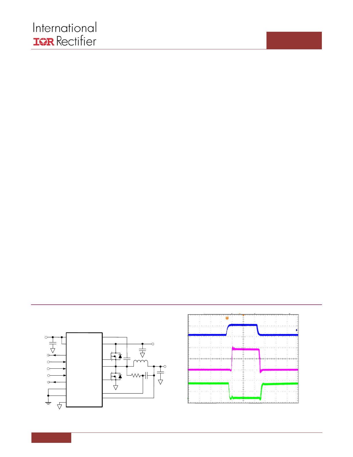
BASIC APPLICATION
SW
PWM
VIN
PGND
VCC
VCC
BOOST
VIN
VOUT
PWM
CSIN+
CSIN‐
4.5V to 7V
LGND
IOUT
IOUT
BBRK#
BBRK#
REFIN
REFIN
4.5V to 14V
IR3535
PHSFLT#
PHSFLT#
GATEL
GATEH
PVCC
TGND
Figure 1: IR3535 Basic Application Circuit
DESCRIPTION
The IR3535 is a high performance, floating N‐channel
MOSFET driver that is optimized for maximum efficiency
delivery of a synchronous buck converter. It is a “Smart”
driver that continually monitors MOSFET conditions,
contains self‐calibrating inductor current sense amplifier,
and provides diode emulation mode with local zero current
detection.
The integrated current sense amplifier achieves superior
current sense accuracy vs. best‐in‐class controller based
inductor DCR sense methods while delivering the clean and
accurate current report information.
The IR patented Body‐Braking
™
feature reduces inductor
to output capacitor energy transfer during load release
which allows the output capacitor bank to be reduced.
Diode emulation mode in the IR3535 alleviates the zero‐
current detection and control burden from the PWM
controller and increases system light load efficiency.
The IR3535 monitors MOSFET conditions and temperature
and reports phase fault if MOSFET short, MOSFET open or
over temperature is detected.
Up to 1.0MHz switching frequency capability enables high
performance transient response, miniaturization of output
inductors, as well as reduced input and output capacitors
while maintaining industry leading efficiency. Solution
size, thermal performance and cost can be optimized by
combining with IR’s DirectFET
™
MOSFETs and utilizing a
dual sided layout.
Figure 2: IR3535 Gate Driver Waveforms
PWM
5V/div
GATEH
10V/div
GATEL
5V/div
100ns/div
March 13, 2013 | FINAL DATASHEET
2
IR3535
Synchronous Buck Converter Driver
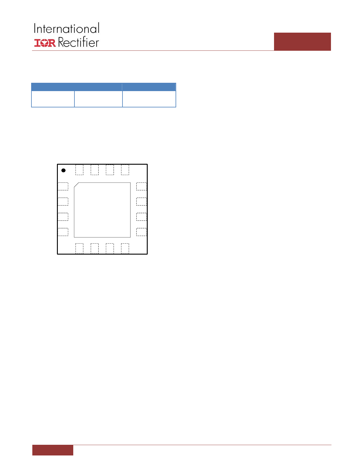
ORDERING INFORMATION
Package
Tape & Reel Qty
Part Number
16 Lead MLPQ
(3 x 3 mm body)
3000
IR3535MTRPBF
PIN DIAGRAM
BBR#
1
LGND
CS
IN
‐
REFIN
2
3
IOUT
GATEH
SW
PGND
GATEL
4
12
11
10
9
5
6
7
8
16
15
14
13
CS
IN
+
VCC
PV
CC
PW
M
PH
SF
LT
#
VI
N
BOOS
T
IR3535
17
TGND
Figure 3: IR3535 Pin Diagram (Top View)
March 13, 2013 | FINAL DATASHEET
3
IR3535
Synchronous Buck Converter Driver
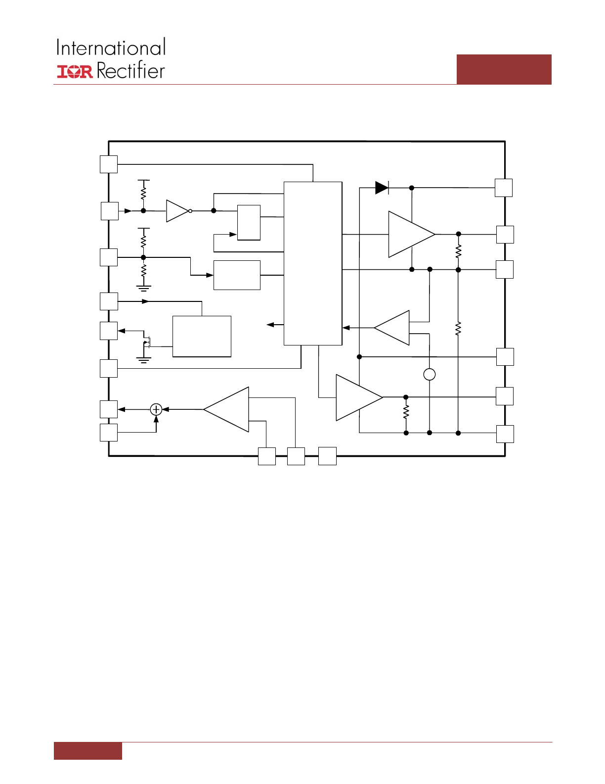
FUNCTIONAL BLOCK DIAGRAM
PWM
11
14
VIN
SW
5
10
CSIN‐
PGND
13 BOOST
Power‐on
Reset
(POR),
3.3V
Reference,
and
Dead‐time
Control
16
IOUT
4
VCC
7
BBR#
1
9
GATEL
Driver
Driver
15
PHSFLT#
6
CSIN+
2
LGND
3
REFIN
Current Sense
Amplifier
MOSFET
& Thermal
Detection
S Q
R
POR
3.3V
VCC
‐
+
3.3V
200k
‐
+
Diode
Emulation
Comparator
IR3535
Offset
‐
+
12 GATEH
8
PVCC
80k
80k
3.3V
Tri‐state
Logic
5.1k
5.1k
X32.5
17
TGND
Figure 4: IR3535 Functional Block Diagram

March 13, 2013 | FINAL DATASHEET
4
IR3535
Synchronous Buck Converter Driver
PIN DESCRIPTIONS
PIN #
PIN NAME
PIN DESCRIPTION
1
BBR#
3.3V logic level input, 7V tolerant, with internal weak pull‐up to 3.3V. Logic “Low” to disable both
MOSFETs. Pulling BBR# low momentarily after VCC passes its UVLO threshold activates the Diode
Emulation Mode.
2
LGND
Ground for control logic and analog circuits. IC substrate is connected to this pin.
3
REFIN
Reference voltage input from the PWM controller. The current sense signal is referenced to the
voltage on this pin. Connect to LGND if the current sense amplifier is not used.
4
IOUT
Voltage on this pin is equal to V(REFIN) + 32.5
*
[V(CSIN+) – V(CSIN‐)]. Float this pin if the current
sense amplifier is not used.
5
CSIN‐
Inverting input to the current sense amplifier. Connect to LGND if the current sense amplifier is not
used.
6
CSIN+
Non‐Inverting input to the current sense amplifier. Connect to LGND if the current sense amplifier
is not used.
7
VCC
Bias voltage for control logic and analog functions.
8
PVCC
Voltage for low‐side MOSFET driver. Internal bootstrap synchronous PFET is connected from this
pin to the BOOST pin. Connect a 1uF capacitor between PVCC and PGND.
9
GATEL
Low‐side driver output and input to GATEH non‐overlap comparator.
10
PGND
Return for low side driver and reference for GATEH non‐overlap comparator.
11
SW
Return for high‐side driver and reference for GATEL non‐overlap comparator.
12
GATEH
High‐side driver output and input to GATEL non‐overlap comparator.
13
BOOST
Supply for high‐side driver. Internal bootstrap synchronous PFET is connected between this pin
and the PVCC pin. Connect a minimum 0.22µF 16Vdc capacitor from BOOST to SW pin.
14
VIN
Power rail input for phase fault detection.
15
PHSFLT#
Open collector output of the phase fault comparators. 7V tolerant, connect to an external
pull‐up resistor. Output is low when a MOSFET fault or over temperature condition is detected.
16
PWM
3.3V logic level Tri‐state PWM input, 7V tolerant. “High” turns the control MOSFET on, and “Low”
turns the synchronous MOSFET on.
“Tri‐state” turns the control MOSFET off without delay.
Depending on the mode the IR3535,
“Tri‐state” either turns the synchronous MOSFET off without
delay in Body‐Braking™ mode or turns synchronous MOEFET off when the current reaches zero in
diode emulation mode. See “Theory of Operation” section for further details.
17
TGND
Ground pad for thermal dissipation. Connected to IC substrate. Connect this pad to ground planes
through four vias.

March 13, 2013 | FINAL DATASHEET
5
IR3535
Synchronous Buck Converter Driver
ABSOLUTE MAXIMUM RATINGS
Stresses beyond those listed under “Absolute Maximum Ratings” may cause permanent damage to the device. These are
stress ratings only and functional operation of the device at these or any other conditions beyond those indicated in the
operational sections of the specifications are not implied.
Storage Temperature Range
‐65°C to 150°C
Operating Junction Temperature
0°C to 150°C
ESD Rating
HBM Class 1C JEDEC Standard
MSL Rating
2
Reflow Temperature
260°C
PIN Number
PIN NAME
V
MAX
V
MIN
I
SOURCE
I
SINK
1
BBR#
8V
‐0.3V
1mA
1mA
2
LGND
n/a
n/a
n/a
n/a
3
REFIN
3.5V
‐0.3V
1mA
1mA
4
IOUT
8V
‐0.3V
5mA
5mA
5
CSIN‐
8V
‐0.3V
1mA
1mA
6
CSIN+
8V
‐0.3V
1mA
1mA
7
VCC
8V
‐0.3V
n/a
15mA
8
PVCC
8V
‐0.3V
n/a
5A for 100ns,
100mA DC
9
GATEL
8V
‐0.3V DC,
‐5V for 100ns
5A for 100ns,
200mA DC
7A for 100ns,
200mA DC
10
PGND
0.3V
‐0.3V
7A for 100ns,
200mA DC
n/a
11
SW
25V
‐0.3V DC,
‐10V for 100ns
5A for 100ns,
100mA DC
n/a
12
GATEH
33V
‐0.3V DC,
‐10V for 100ns
5A for 100ns,
100mA DC
5A for 100ns,
100mA DC
13
BOOST
33V
‐0.3V
1A for 100ns,
100mA DC
3A for 100ns,
100mA DC
14
VIN
16V
‐0.3V
n/a
1mA
15
PHSFLT#
8V
‐0.3V
1mA
20mA
16
PWM
8V
‐0.3V
1mA
1mA
Note:
1. Maximum GATEH – SW = 8V
2.
Maximum BOOST – GATEH = 8V

March 13, 2013 | FINAL DATASHEET
6
IR3535
Synchronous Buck Converter Driver
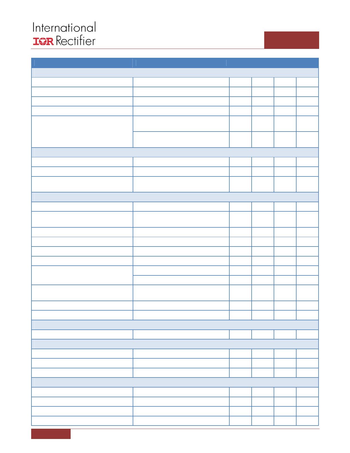
ELECTRICAL SPECIFICATIONS
RECOMMENDED OPERATING CONDITIONS FOR RELIABLE OPERATION WITH MARGIN
SYMBOL
MIN
MAX
UNITS
Recommended VIN Range
VIN
4.5
14
V
Recommended VCC Range
VCC
4.5
7
V
Recommended REFIN Range (V
CC
= 4.5V to 5.5V)
REFIN
0.25
2.0
V
Recommended REFIN Range (V
CC
= 5.5V to 7V)
REFIN
0.25
3.3
V
Recommended Switching Frequency
F
SW
200
1000
kHz
Recommended Operating Junction Temperature
T
J
0
125
°C
ELECTRICAL CHARACTERISTICS
The electrical characteristics involve the spread of values guaranteed within the recommended operating conditions.
Typical values represent the median values, which are related to 25°C.
C
GATEH
= 3.3nF, C
GATEL
= 6.8nF (unless otherwise specified).
PARAMETER
CONDITIONS
MIN
TYP
MAX
UNIT
Gate Drivers
GATEH Source Resistance
BOOST – SW = 7V
670
MΩ
GATEH Sink Resistance
BOOST – SW = 7V
670
MΩ
GATEL Source Resistance
PVCC – PGND = 7V
670
MΩ
GATEL Sink Resistance
PVCC – PGND = 7V
300
MΩ
GATEH Source Current
BOOST = 7V, GATEH = 2.5V, SW = 0V
3
A
GATEH Sink Current
BOOST = 7V, GATEH = 2.5V, SW = 0V
4
A
GATEL Source Current
PVCC = 7V, GATEL = 2.5V, SW = 0V
4
A
GATEL Sink Current
PVCC = 7V, GATEL = 2.5V, SW = 0V
6
A
GATEH Rise Time
BOOST – SW = 7V, measure 1V to 4V
transition time
5
10
ns
GATEH Fall Time
BOOST – SW = 7V, measure 4V to 1V
transition time
4
8
ns
GATEL Rise Time
PVCC – PGND = 7V, measure 1V to 4V
transition time
10
20
ns
GATEL Fall Time
PVCC – PGND = 7V, measure 4V to 1V
transition time
5
10
ns
GATEL Low to GATEH High Delay
BOOST = PVCC = 7V, SW = PGND = 0V,
measure time from GATEL falling to 1V to
GATEH rising to 1V
10
15
30
ns
GATEH Low to GATEL High Delay
BOOST = PVCC = 7V, SW = PGND = 0V,
measure time from GATEH falling to 1V to
GATEL rising to 1V
10
15
30
ns
Disable Pull Down Resistance
GATEH to SW, GATEL to PGND
30
80
130
KΩ
March 13, 2013 | FINAL DATASHEET
7
IR3535
Synchronous Buck Converter Driver
PARAMETER
CONDITIONS
MIN
TYP
MAX
UNIT
PWM Comparator
High Side Switch Threshold
PWM Low or PWM Tri‐State to High
2.5
V
Low Side Switch Threshold
PWM High or PWM Tri‐State to Low
0.8
V
PWM Tri‐State Float Voltage
Floating
1.2
1.65
2.1
V
Hysteresis
Active to Tri‐State to Active, Note 1
65
76
100
mV
Tri‐State Propagation Delay Time
C
PWM
= 20pF, measure from V(PWM) = 0V
to GATEL < 1V
190
ns
C
PWM
= 20pF, measure from V(PWM) = 5V
release to GATEH < 1V
380
ns
PWM Input
Sinking Impedance
3.67
5.1
8.7
KΩ
Source Impedance
3.67
5.1
8.7
KΩ
GATEH Turn‐Off Propagation Delay
Measure from V(PWM) falling edge to
GATEH < 1V
25
45
ns
Current Sense Amplifier
CSIN+/‐ Bias Current
‐100
0
100
nA
Input Offset Voltage
CSIN+ = CSIN‐ = REFIN, measure input
referred offset from REFIN
‐750
750
µV
Calibrated Input Offset Voltage
Self‐calibrated offset, Note 1
‐450
0
450
µV
Gain
0.5V ≤ V(REFIN) < 2.25
30
32.5
35
V/V
Unity Gain Bandwidth
C(IOUT) = 10pF, measure at IOUT. Note 1
4.8
6.8
8.8
MHz
Slew Rate
6
V/µs
Differential Input Range
0.8V ≤ V(REFIN) ≤ 2.25V, Note 1
‐10
25
mV
0.25V ≤ V(REFIN) ≤ 0.8V, Note 1
‐5
25
mV
Common Mode Input Range
0
VCC –
2.5
V
Output Impedance
62
200
Ω
IOUT Sink Current
Driving external 3 kΩ
0.5
0.8
1.1
mA
Bootstrap Diode
Forward Voltage
I(BOOST) = 30mA, VCC = 6.8V
360
520
960
mV
Digital Output ― Phase Fault
VOH
HIGH Level Pull‐Up Voltage
7
V
VOL
I(PHSFLT#) = 4mA
150
300
mV
Leakage Current
V(PHSFLT#) = 5.5V
0
1
µA
Phase Fault Detection
Top Side Threshold
Measure from Vin to SW
1.9
2.2
2.5
V
Bottom Side Threshold
150
200
250
mV
Bottom FET Open Threshold
‐250
‐215
‐180
mV
Propagation Delay
PWM High to PWM Low Cycles
15
Cycles
March 13, 2013 | FINAL DATASHEET
8
IR3535
Synchronous Buck Converter Driver
PARAMETER
CONDITIONS
MIN
TYP
MAX
UNIT
Operating Bias Voltage
4.5
7
V
Digital Input ― BBR#
VIL
Input Low Threshold
0.8
V
VIH
Input High Threshold
2.0
V
Internal Pull Up Resistance
VCC > UVLO
69
200
340
KΩ
Internal Pull Up Voltage
VCC > UVLO
3.3
V
General
VCC Supply Current
4
8
12
mA
VIN Supply Curent
4.5 ≤ V(VIN) ≤ 14V
0.05
0.15
0.4
mA
Switch Node Bias Current
5
mA
BOOST Supply Current
4.75 ≤ V(BOOST) – V(SW) ≤ 7V
0.5
1.5
3
mA
REFIN Bias Current
‐1.5
0
1
µA
SW Floating Voltage
CSIN‐ tied to SW, PWM Tri‐State
0.1
0.3
0.4
V
Diode Emulation Mode Comparator
Input Offset Voltage
Note 2
‐12
‐3
3
mV
Leading Edge Blanking Time
V(GATEL) > 1V Starts Timer, Note 1
100
150
200
ns
Propagation Delay
Blanking Expired, +2.5mV overdrive to
V(GATEL) < 1V, Note 1
41
50
ns
Negative Current Time‐Out
PWM = Tri‐State, V(SW) < = ‐10mV
20
30
45
µs
VCC Under Voltage Lockout
Start
3.3
3.7
4.1
V
Stop
3
3.4
3.8
V
Hysteresis
0.25
0.35
0.45
V
Thermal Flag
Rising Threshold
PHSFLT# Drives Low. Note 1
115
°C
Falling Threshold
Note 1
95
°C
Note:
1. Guaranteed by design but not tested in production
2.
The Diode Emulation Mode (DEM) comparator measures the SW against PGND. The input offset is biased slightly to the negative so
that a slightly positive current in the synchronous MOSFET is treated as zero current to accommodate propagation delays and
untrimmed accuracy.
March 13, 2013 | FINAL DATASHEET
9
IR3535
Synchronous Buck Converter Driver
THEORY OF OPERATION
DESCRIPTION
The IR3535 is a synchronous buck driver which provides
system designers with ease of use and flexibility required
in cutting edge CPU, GPU and memory power delivery
designs. The IR3535 is designed to work with a controller
that provides the PWM signal. The IR3535 incorporates a
continuously self‐calibrated current sense amplifier,
optimized for use with inductor DCR sensing. The current
sense amplifier provides signal gain and noise immunity,
providing multiphase systems with a superior design
toolbox for programmed impedance designs.
The IR3535 also provides a phase fault signal capable of
detecting open or shorted MOSFETs, or an over‐
temperature condition in the vicinity of the driver.
The IR3535 accepts an active low Body‐Braking™ input
which disables the output MOSFETs to enhance transient
performance or provide a high impedance output.
The IR3535 PWM input is compatible with 3.3V logic and
7V tolerant. It accepts 3‐level PWM input signals, with a
diode emulation feature when the PWM signal is floated,
allowing designers to maximize system efficiency at light
loads without compromising transient performance.
BODY‐BRAKING™ MODE
There are two ways to place the IR3535 in Body‐Braking™
mode, in which two MOSFETs are turned off.
Pulling BBR# low forces the IR3535 into Body‐Braking™
mode rapidly, which is used to enhance transient response
after load release or provide a high impedance output.
If the BBR# input is high and has not been low since power
on, the Body‐Braking™ is activated when the PWM input
enters the tri‐state region, which is withing a range around
1.65V. The Body‐Braking™ response is slower due to the
hold‐off time created by the paracitic capacitor with pull‐
up or pull‐down resistor at PWM pin. For better
performance, no more than 100pF parasitic capacitive load
should be present on the PWM line of IR3535.
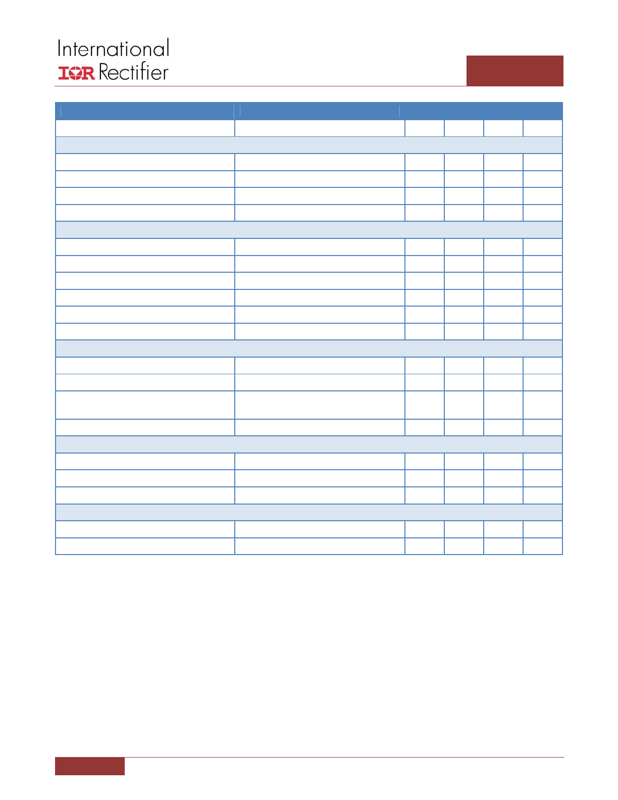
DIODE EMULATION MODE
An additional feature of the IR3535 is diode emulation
mode. This function improves efficiency by preventing
negative inductor current from flowing in the synchronous
MOSFET.
As shown in Figure 5, when the PWM input enters the tri‐
state region the control MOSFET is turned off first, and the
synchronous MOSFET is initially turned on and then is
turned off when the output current reaches zero. If the
sensed output current does not reach zero within a set
amount of time the gate driver will assume that the output
is de‐biased and turn off the synchronous MOSFET,
allowing the switch node to float.
This is in contrast to the Body‐Braking® mode shown in
Figure 6, where GATEL follows PWM input. The Schottky
diode in parallel with the synchronous MOSFET conducts
for a longer period of time and therefore lowers the light
load efficiency.
Figure 5: Diode Emulation Mode
Figure 6: Body‐Braking® Mode
PWM
2V/div
SW
5V/div
400ns/div
GAETL
10V/div
PWM
2V/div
SW
5V/div
400ns/div
GATEL
10V/div
March 13, 2013 | FINAL DATASHEET
10
IR3535
Synchronous Buck Converter Driver
The zero current detection circuit in the IR3535 is
independent of the current sense amplifier and therefore
still functions even if the current sense amplifier is not
used. As shown in Figure 4, an offset is added to the diode
emulation comparator so that a slightly positive output
current in the inductor and synchronous MOSFET is treated
as zero current to accommodate propagation delays,
preventing any negative current flowing in the
synchronous MOSFET. This causes the Schottky diode in
parallel with the synchronous MOSFET to conduct before
the inductor current actually reaches zero, and the
conduction time increases with inductance of the output
inductor.
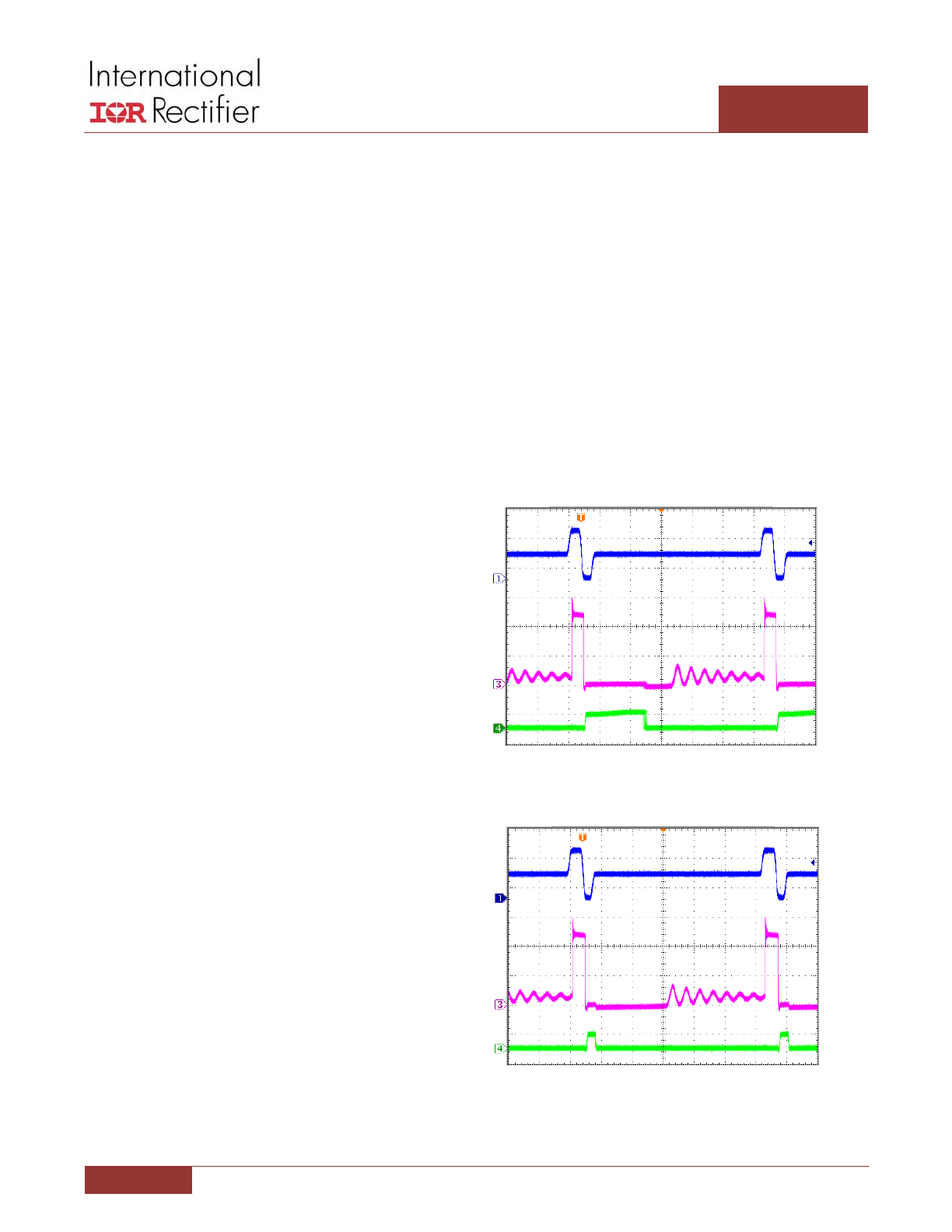
To set the IR3535 in diode emulation mode, the BBR# pin
must be toggled low at least once after the VCC passes its
UVLO threshold during power up. One simple way is to use
the internal BBR# pull‐up resistor (200kΩ typical) with an
external capacitor from BBR# pin to LGND. To ensure the
diode emulation mode is properly set, the BBR# voltage
should be lower than 0.8V when the VCC voltage passes its
UVLO threshold (3.3V minimum and 3.7V typical), as
shown in Figure 7. A digital signal from the PWM controller
can also be used to set the diode emulation mode. The
BBR# signal can either be pulled low for at least 20ns after
the VCC passes its UVLO threshold, as shown in Figure 8, or
be pulled low before VCC power up and then released
after the VCC passes its UVLO threshold, as shown in
Figure 9.
Once the diode emulation mode is set, it cannot be reset
until the VCC power is recycled.
TRI‐STATE GATE DRIVERS
The gate drivers can deliver up to 4A peak current and 6A
sink current for low side driver. An adaptive non‐overlap
circuit monitors the voltage on the internal GATEH and
GATEL pins to prevent MOSFET shoot‐through current
while minimizing body diode conduction. Tri‐state
operation prevents negative inductor current and negative
output voltage during power‐down. The gate driver
incorporates pull down resistors on the MOSFET gates to
prevent spurious turn‐on of the output stage even when
the IC is off and there is a high dV/dt event on the VIN
supply rail. The gate drivers pull low if the supply voltages
are below the normal operating range.
PHASE FAULT CIRCUIT AND THERMAL
FLAG CIRCUIT (PHSFLT#)
The IR3535 phase fault circuit monitors the switch node
with respect to VIN and ground to determine whether
Figure 7: Diode Emulation Setup through BBR# Capacitor
Figure 8: Diode Emulation Setup through BBR# Input
Figure 9: Diode Emulation Setup through BBR# Input
there is a defective MOSFET in the converter. The output
of the PHSFLT# is high during normal operation and
becomes low when there is a fault. The driver monitors the
VCC
2V/div
BBR#
1V/div
2ms/div
SW
10V/div
VCC
2V/div
BBR#
2V/div
4ms/div
VCC
2V/div
BBR#
2V/div
4ms/div