
www.irf.com
14-Aug-09
© 2009 International Rectifier
1
HALF-BRIDGE GATE DRIVER IC
Features
•
Floating channel up to 600 V or 1200 V
•
Soft over-current shutdown
•
Synchronization signal to synchronize shutdown with the other phases
•
Integrated desaturation detection circuit
•
Two stage turn on output for di/dt control
•
Separate pull-up/pull-down output drive pins
•
Matched delay outputs
•
Undervoltage lockout with hysteresis band
•
Lead free
Description
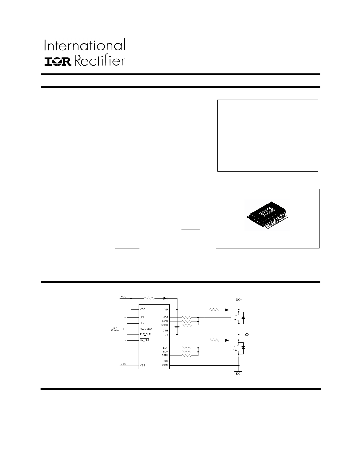
The IR2114/IR2214 gate driver family is suited to drive a single half bridge in
power switching applications. These drivers provide high gate driving
capability (2 A source, 3 A sink) and require low quiescent current, which
allows the use of bootstrap power supply techniques in medium power
systems. These drivers feature full short circuit protection by means of power
transistor desaturation detection and manage all half-bridge faults by
smoothly turning off the desaturated transistor through the dedicated soft
shutdown
pin,
therefore
preventing
over-voltages
and
reducing
electromagnetic emissions. In multi-phase systems, the IR2114/IR2214
drivers communicate using a dedicated local network (SY_FLT and
FAULT/SD signals) to properly manage phase-to-phase short circuits. The
system controller may force shutdown or read device fault state through the
3.3 V compatible CMOS I/O pin (FAULT/SD). To improve the signal immunity
from DC-bus noise, the control and power ground use dedicated pins
enabling low-side emitter current sensing as well. Undervoltage conditions in
floating and low voltage circuits are managed independently.
Product Summary
V
OFFSET
600 V or
1200 V max.
I
O
+/- (min)
1.0 A / 1.5 A
V
OUT
10.4 V – 20 V
Deadtime matching (max)
75 ns
Deadtime (typ)
330
ns
Desat blanking time (typ)
3
µs
DSH, DSL input voltage
threshold (typ)
8.0 V
Soft shutdown time (typ)
9.25 µs
Package
24-Lead SSOP
Typical connection
IR2114SSPbF/IR2214SSPbF
Data Sheet No. PD60213 revL
IR2114/IR2214SSPbF
www.irf.com
© 2009 International Rectifier
2
Recommended Operating Conditions
For proper operation the device should be used within the recommended conditions. All voltage parameters are absolute
voltages referenced to V
SS
. The V
S
offset rating is tested with all supplies biased at a 15 V differential.
Symbol
Definition
Min.
Max.
Units
V
B
High side floating supply voltage
†
V
S
+ 11.5
V
S
+ 20
IR2114
V
SS
600
V
S
High side floating supply offset voltage
††
IR2214
V
SS
1200
V
HO
High side output voltage (HOP, HON and SSDH)
V
S
V
S
+ 20
V
LO
Low side output voltage (LOP, LON and SSDL)
V
COM
V
CC
V
CC
Low side and logic fixed supply voltage (Note 1)
11.5
20
COM
Power ground
-5
5
V
IN
Logic input voltage (HIN, LIN and FLT_CLR)
V
SS
V
CC
V
FLT
Fault input/output voltage (FAULT/SD and SY_FLT)
V
SS
V
CC
V
DSH
High side DS pin input voltage
V
S
- 2.0
V
B
V
DSL
Low side DS pin input voltage
V
COM
- 2.0
V
CC
V
t
PWHIN
High side pulse width for HIN input
1
µs
T
A
Ambient temperature
-40
125
°C
†
While internal circuitry is operational below the indicated supply voltages, the UV lockout disables the output
drivers if the UV thresholds are not reached. A minimum supply voltage of 8V is recommended for the driver
to operate safely under switching conditions at VS pin (please refer to the “start-up sequence” in application
section of this document)
††
Logic operational for V
S
from V
SS
-5 V to V
SS
+600 V or 1200 V. Logic state held for V
S
from V
SS
-5 V to V
SS
-
V
BS
. For a negative spike on V
B
(referenced to V
SS
) of less than 200ns the IC will withstand a sustained peak
of -40V under normal operation and an isolated event of up to -70V peak spike (please refer to the Design
Tip DT97-3 for more details).
Absolute Maximum Ratings
Absolute maximum ratings indicate sustained limits beyond which damage to the device may occur. All voltage
parameters are absolute voltages referenced to V
SS
, all currents are defined positive into any lead The thermal resistance
and power dissipation ratings are measured under board mounted and still air conditions.
Symbol
Definition
Min.
Max.
Units
V
S
High side offset voltage
V
B
- 25
V
B
+ 0.3
IR2114
-0.3
625
V
B
High side floating supply voltage
IR2214
-0.3
1225
V
HO
High side floating output voltage (HOP, HON and SSDH)
V
S
- 0.3
V
B
+ 0.3
V
CC
Low side and logic fixed supply voltage
-0.3
25
COM
Power ground
V
CC
- 25
V
CC
+ 0.3
V
LO
Low side output voltage (LOP, LON and SSDL)
V
COM
-0.3
V
CC
+ 0.3
V
IN
Logic input voltage (HIN, LIN and FLT_CLR)
-0.3
V
CC
+ 0.3
V
FLT
Fault input/output voltage (FAULT/SD and SY_FLT)
-0.3
V
CC
+ 0.3
V
DSH
High side DS input voltage
V
S
-3
V
B
+ 0.3
V
DSL
Low side DS input voltage
V
COM
-3
V
CC
+ 0.3
V
dVs/dt
Allowable offset voltage slew rate
—
50
V/ns
P
D
Package power dissipation @ T
A
≤ 25 °C
—
1.5
W
Rth
JA
Thermal resistance, junction to ambient
—
65
°C/W
T
J
Junction temperature
—
150
T
S
Storage temperature
-55
150
T
L
Lead temperature (soldering, 10 seconds)
—
300
°C
IR2114/IR2214SSPbF
www.irf.com
© 2009 International Rectifier
3
Static Electrical Characteristics
V
CC
= 15 V, V
SS
= COM = 0 V, V
S
= 600 V or 1200 V and T
A
= 25 °C unless otherwise specified.
Pins: V
CC
, V
SS
, V
B
, V
S
(refer to Fig. 1)
Symbol
Definition
Min Typ Max Units
Test Conditions
V
CCUV+
V
CC
supply undervoltage positive going threshold
9.3 10.2 11.4
V
CCUV-
V
CC
supply undervoltage negative going threshold
8.7
9.3
10.3
V
CCUVH
V
CC
supply undervoltage lockout hysteresis
—
0.9
—
V
BSUV+
(V
B
-V
S
) supply undervoltage positive going threshold
9.3 10.2 11.4
V
BSUV-
(V
B
-V
S
) supply undervoltage negative going threshold
8.7
9.3
10.3
V
S
= 0 V, V
S
= 600 V
or 1200 V
V
BSUVH
(V
B
-V
S
) supply undervoltage lockout hysteresis
—
0.9
—
V
I
LK
Offset supply leakage current
—
—
50
V
B
= V
S
= 600 V or
1200 V
I
QBS
Quiescent V
BS
supply current
—
400
800
µA
V
IN
= 0 V or 3.3 V
I
QCC
Quiescent V
CC
supply current
—
0.7
2.5
mA
no load
Pins: HIN, LIN, FLTCLR, FAULT/SD, SY_FLT (refer to Fig. 2, 3)
Symbol
Definition
Min
Typ
Max Units
Test Conditions
V
IH
Logic "1" input voltage
2.0
—
—
V
IL
Logic "0" input voltage
—
—
0.8
V
IHSS
Logic input hysteresis
0.2
0.4
—
V
V
CC
= V
CCUV-
to 20 V
Logic “1” input bias current (HIN, LIN, FLTCLR)
—
330
—
I
IN+
Logic “0” input bias current (FAULT/SD, SY_FLT)
0
—
1
V
IN
= 3.3 V
Logic “0” input bias current
-1
—
0
I
IN-
Logic “1” input bias current (FAULT/SD, SY_FLT)
-1
—
0
µA
V
IN
= 0 V
R
ON,FLT
FAULT/SD open drain resistance
—
60
—
R
ON,SY
SY_FLT open drain resistance
—
60
—
Ω
PW≤ 7 µs
Pins: DSL, DSH (refer to Fig. 4)
V
DESAT
, I
DS
and I
DSB
parameters are referenced to COM and V
S
respectively for DSL and DSH.
Symbol
Definition
Min Typ Max Units
Test Conditions
V
DESAT+
High desat input threshold voltage
7.2 8.0 8.8
V
DESAT-
Low desat input threshold voltage
6.3 7.0 7.7
V
DSTH
Desat input voltage hysteresis
— 1.0 —
V
See Figs. 4,16
I
DS+
High DSH or DSL input bias current — 21 —
V
DESAT
= V
CC
or V
BS
I
DS
-
Low DSH or DSL input bias current
— -160 —
µA
V
DESAT
= 0 V
IR2114/IR2214SSPbF
www.irf.com
© 2009 International Rectifier
4
Pins: HOP, LOP (refer to Fig. 5)
Symbol
Definition
Min Typ Max Units Test Conditions
V
OH
High level output voltage, V
B
– V
HOP
or V
CC
–V
LOP
—
40
300
mV
I
O
= 20 mA
I
O1+
Output high first stage short circuit pulsed current
1
2
—
V
HOP/LOP
= 0 V, H
IN
or L
IN
= 1, PW≤
200 ns, resistive
load, see Fig. 8
I
O2+
Output high second stage short circuit pulsed current
0.5
1
—
A
V
HOP/LOP
= 0 V, H
IN
or L
IN
= 1,
400 ns ≤PW≤ 10
µs, resistive load,
see Fig. 8
Pins: HON, LON, SSDH, SSDL (refer to Fig. 6)
Symbol
Definition
Min Typ Max Units Test Conditions
V
OL
Low level output voltage, V
HON
or V
LON
—
45
300
mV
I
O
= 20 mA
R
ON,SSD
Soft Shutdown on resistance
†
—
90
—
Ω
PW≤ 7 µs
I
O-
Output low short circuit pulsed current
1.5
3
—
A
V
HOP/LOP
= 15 V,
H
IN
or L
IN
= 0, PW≤
10 µs
†
SSD operation only
IR2114/IR2214SSPbF
www.irf.com
© 2009 International Rectifier
5
AC Electrical Characteristics
V
CC
= V
BS
= 15 V, V
S
= V
SS
and T
A
= 25 °C unless otherwise specified.
Symbol
Definition
Min.
Typ. Max. Units
Test Conditions
t
on
Turn on propagation delay
220
440
660
t
off
Turn off propagation delay
220
440
660
t
r
Turn on rise time (C
LOAD
=1 nF)
—
24
—
t
f
Turn off fall time (C
LOAD
=1 nF)
—
7
—
V
IN
= 0 & 1, V
S
= 0 V to 600 V
or 1200 V,
HOP shorted to HON, LOP
shorted to LON, Fig. 7
t
on1
Turn on first stage duration time
120
200
280
Fig. 8
t
DESAT1
DSH to HO soft shutdown propagation delay at HO
turn on
2000 3300 4600
V
HIN
= 1 V
t
DESAT2
DSH to HO soft shutdown propagation delay after
blanking
1050
—
—
V
DESAT
= 15 V, Fig. 10
t
DESAT3
DSL to LO soft shutdown propagation delay at LO
turn on
2000 3300 4600
V
LIN
= 1 V
t
DESAT4
DSL to LO soft shutdown propagation delay after
blanking
1050
—
—
V
DESAT
= 15 V, Fig. 10
t
DS
Soft shutdown minimum pulse width of desat
1000
—
—
Fig. 9
t
SS
Soft shutdown duration period
5700 9250 13500
V
DS
=15 V, Fig. 9
t
SY_FLT,
DESAT1
DSH to SY_FLT propagation delay at HO turn on
—
3600
—
V
HIN
= 1 V
t
SY_FLT,
DESAT2
DSH to SY_FLT propagation delay after blanking
1300
—
—
V
DS
= 15 V, Fig. 10
t
SY_FLT
,
DESAT3
DSL to SY_FLT propagation delay at LO turn on
—
3050
—
V
LIN
= 1 V
t
SY_FLT
,
DESAT4
DSL to SY_FLT propagation delay after blanking
1050
—
—
V
DESAT
=15 V, Fig. 10
t
BL
DS blanking time at turn on
—
3000
—
V
HIN
= V
LIN
= 1 V, V
DESAT
=15 V,
Fig. 10
Deadtime/Delay Matching Characteristics
DT
Deadtime
—
330
—
Fig. 11
MDT
Deadtime matching, MDT=DTH-DTL
—
—
75
External DT = 0 s, Fig. 11
PDM
Propagation delay matching,
Max (ton, toff) – Min (ton, toff)
—
—
75
ns
External DT > 500 ns, Fig. 7
IR2114/IR2214SSPbF
www.irf.com
© 2009 International Rectifier
6
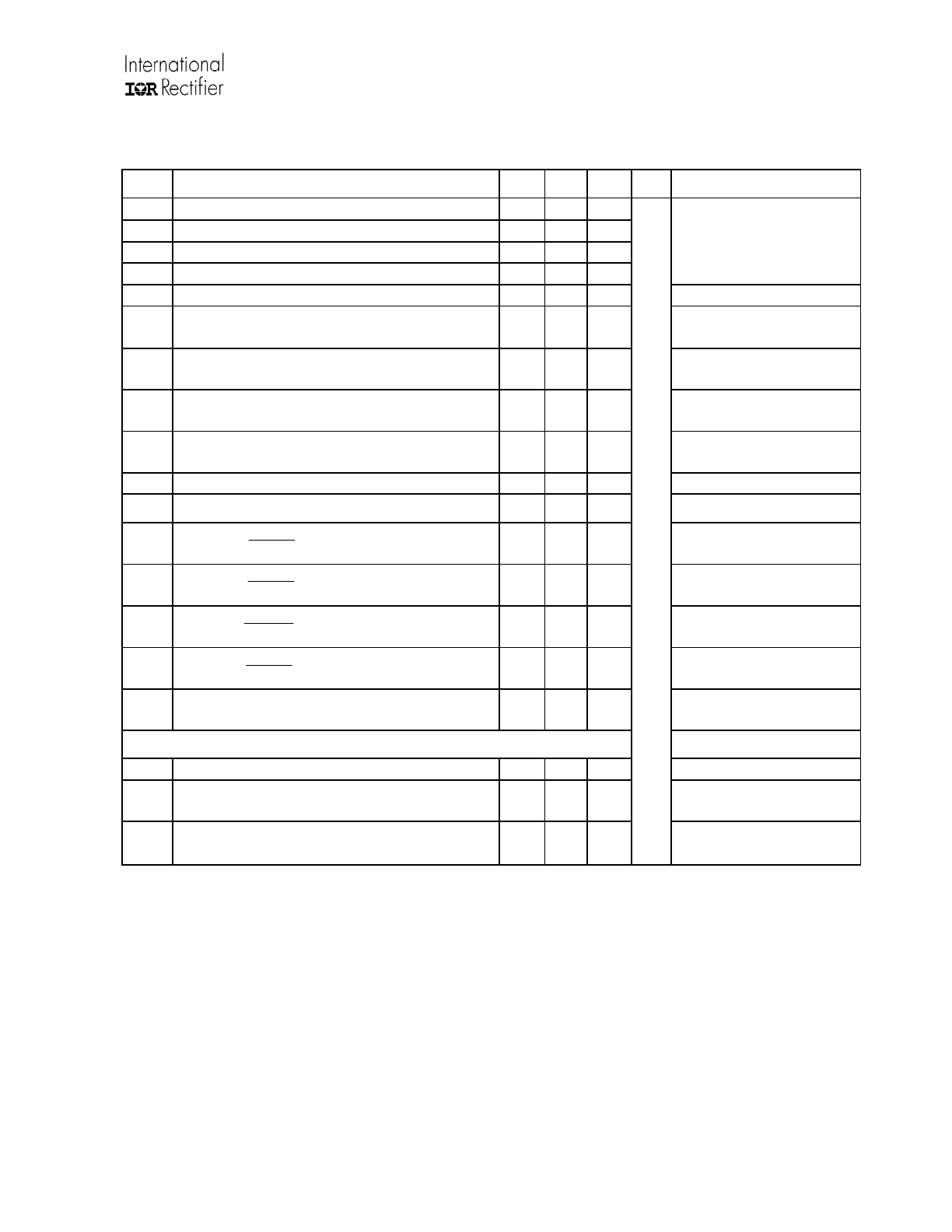
Figure 1:
Undervoltage Diagram Figure 2: HIN, LIN and FLTCLR Diagram
Figure 3:
FAULT/SD and SY_FLT Diagram Figure 4: DSH and DSL Diagram
Figure 5:
HOP and LOP Diagram Figure 6: HON, LON, SSDH and SSDL Diagram
V
CC
/V
B
V
CCUV
/V
BSUV
V
SS
/V
S
comparator
UV
internal
signal
HIN/LIN/
FLTCLR
V
SS
schmitt
trigger
10k
internal
signal
LOP/HOP
V
CC
/V
B
on/off
internal signal
V
OH
200ns
oneshot
SSDL/SSDH
COM/V
S
on/off
internal signal
R
ON,SSD
LON/HON
desat
internal signal
V
OL
DSL/DSH
V
DESAT
COM/V
S
comparator
100k
700k
V
CC
/V
BS
SSD
internal
signal
FAULT/SD
SY_FLT
V
SS
schmitt
trigger
R
ON
fault/hold
internal signal
IR2114/IR2214SSPbF
www.irf.com
© 2009 International Rectifier
7
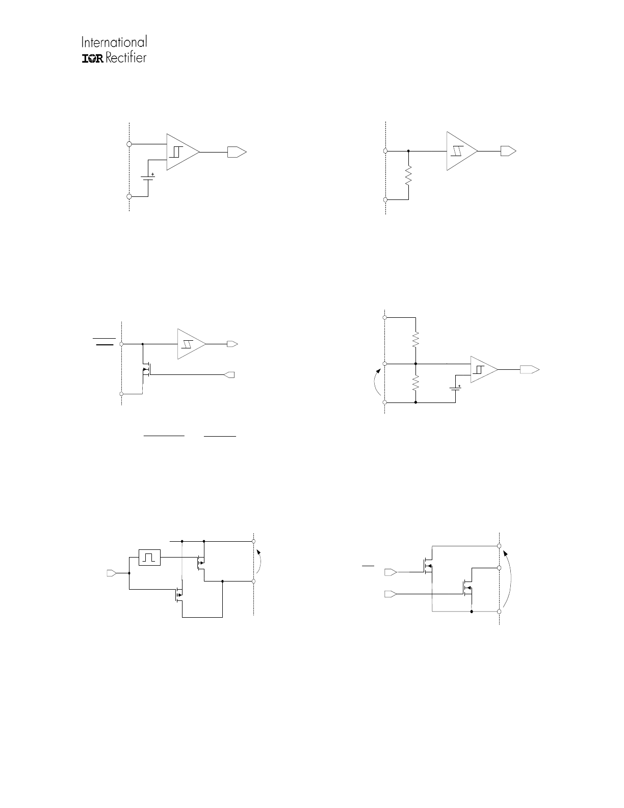
HIN
LIN
HO (HOP=HON)
LO (LOP=LON)
10%
3.3V
PW
in
PW
out
10%
90%
90%
50%
50%
t
on
t
r
t
off
t
f
Figure 7:
Switching Time Waveforms
Ton1
Io1+
Io2+
Figure 8:
Output Source Current
HIN/LIN
HO/LO
8V
8V
t
SS
t
DESAT
3.3V
DSH/DSL
t
DS
SSD Driver Enable
Figure 9:
Soft Shutdown Timing Waveform
IR2114/IR2214SSPbF
www.irf.com
© 2009 International Rectifier
8
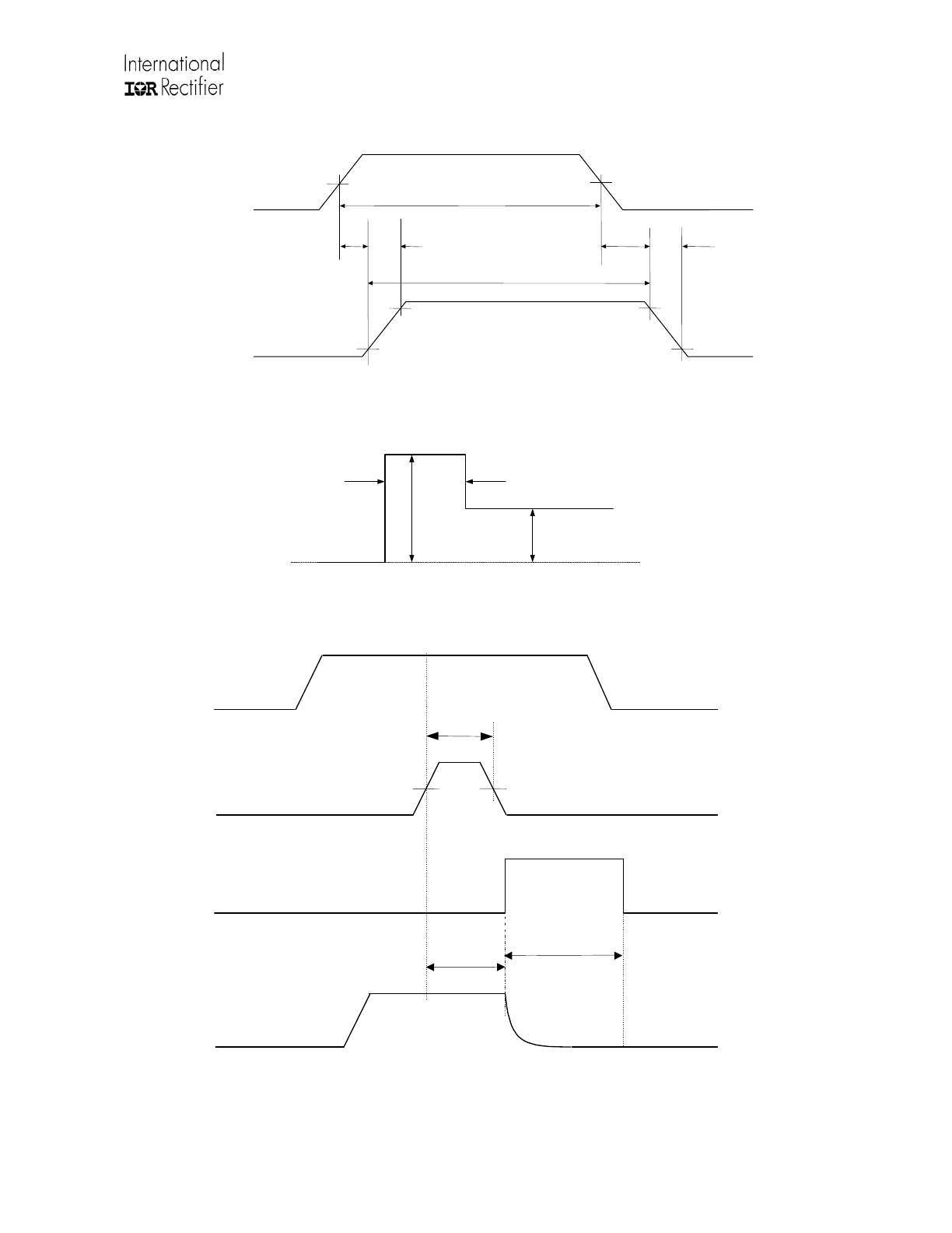
HIN
DSH
SY_FLT
t
DESAT1
8V
50%
t
SY_FLT,DESAT1
HON
90%
50%
t
BL
FAULT/SD
FLTCLR
SoftShutdown
LIN
LON
90%
SoftShutdown
t
DESAT2
8V
t
SY_FLT,DESAT2
50%
t
BL
DSL
90%
50%
t
BL
SoftShutdown
90%
SoftShutdown
50%
t
BL
8V
8V
50%
t
SY_FLT,DESAT3
t
SY_FLT,DESAT4
t
DESAT3
t
DESAT4
50%
50%
Turn-On Propagation Delay
Turn-On Propagation Delay
90%
Turn_Off propagation Delay
50%
90%
50%
50%
10%
10%
Figure 10:
Desat Timing
HIN
LIN
HO (HOP=HON)
LO (LOP=LON)
DTH
DTL
50%
50%
50%
50%
50%
50%
MDT=DTH-DTL
Figure 11:
Internal Deadtime Timing
IR2114/IR2214SSPbF
www.irf.com
© 2009 International Rectifier
9
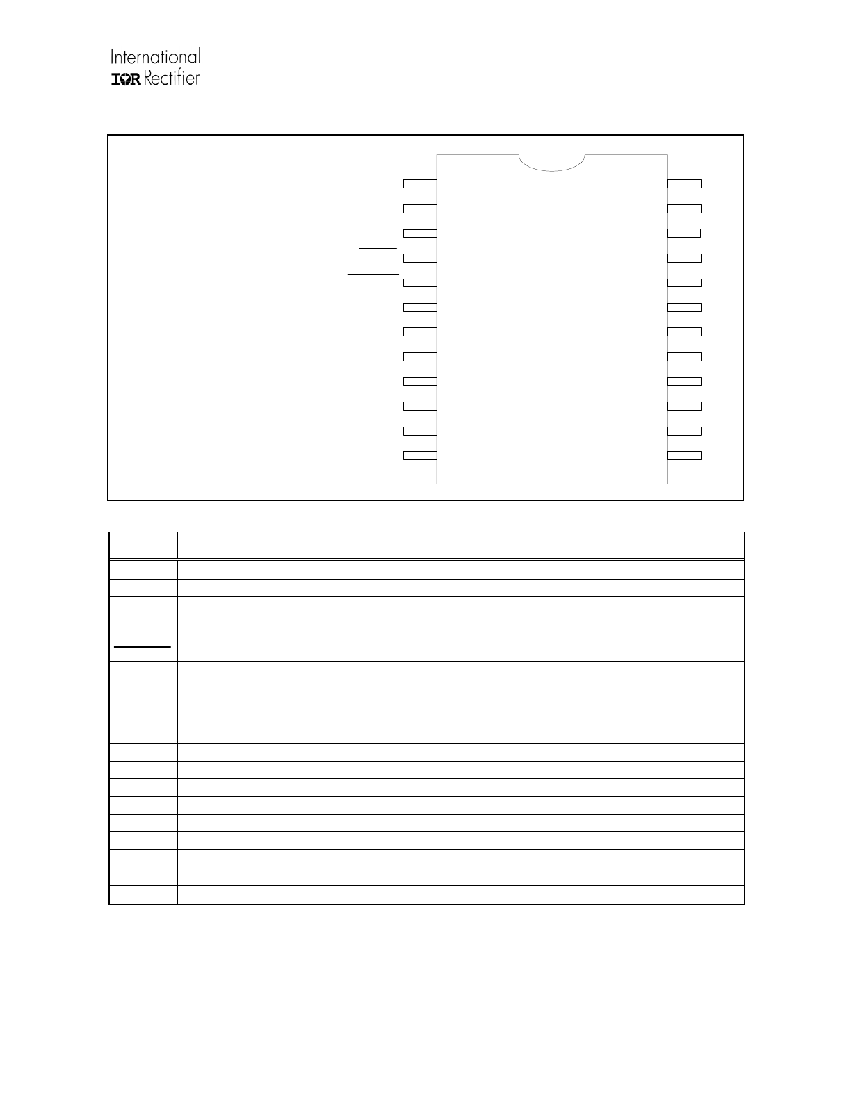
Lead Assignments
24-Lead SSOP
Lead Definitions
Symbol
Description
V
CC
Low side gate driver supply
V
SS
Logic ground
HIN
Logic input for high side gate driver outputs (HOP/HON)
LIN
Logic input for low side gate driver outputs (LOP/LON)
FAULT/SD
Dual function (in/out) active low pin. Refer to Figs. 15, 17, and 18. As an output, indicates fault condition.
As an input, shuts down the outputs of the gate driver regardless H
IN
/L
IN
status.
SY_FLT
Dual function (in/out) active low pin. Refer to Figs. 15, 17, and 18. As an output, indicates SSD sequence
is occurring. As an input, an active low signal freezes both output status.
FLT_CLR
Fault clear active high input. Clears latched fault condition (see Fig. 17)
LOP
Low side driver sourcing output
LON
Low side driver sinking output
DSL
Low side IGBT desaturation protection input
SSDL
Low side soft shutdown
COM
Low side driver return
V
B
High side gate driver floating supply
HOP
High side driver sourcing output
HON
High side driver sinking output
DSH
High side IGBT desaturation protection input
SSDH
High side soft shutdown
V
S
High side floating supply return
SSOP24
1
12
24
13
SSDL
FLT_CLR
HIN
COM
SY_FLT
LON
FAULT/SD
VSS
LOP
VCC
DSL
HOP
SSDH
HON
N.C.
VS
N.C.
DSH
VB
N.C.
N.C.
N.C.
N.C.
LIN
IR2114/IR2214SSPbF
www.irf.com
© 2009 International Rectifier
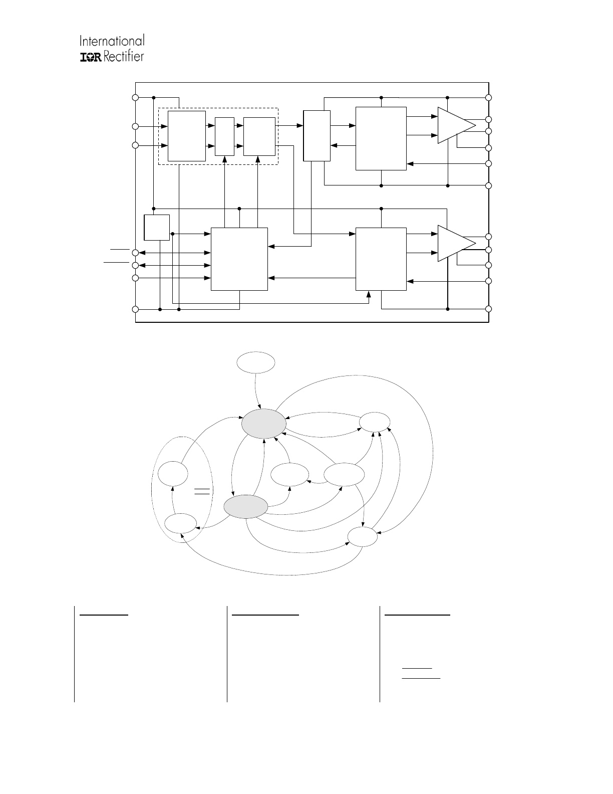
10
SCHMITT
TRIGGER
INPUT
SHOOT
THROUGH
PREVENTION
(DT) Deadtime
LEVEL
SHIFTERS
LATCH
LOCAL DESAT
PROTECTION
SOFT SHUTDOWN
UV_VBS DETECT
di/dt control
Driver
UV_VCC
DETECT
LOCAL DESAT
PROTECTION
SOFTSHUTDOWN
di/dt control
Driver
on/off
on/off
desat
soft
shutdown
on/off
soft
shutdown
on/off (HS)
DesatHS
DesatLS
on/off (LS)
H
a
rd
S
h
u
tD
o
w
n
in
te
rn
a
l H
o
ld
SD
FAULT LOGIC
managemend
(See figure 14)
UV_VCC
VB
HOP
HON
SSDH
DSH
VS
LOP
LON
SSDL
DSL
COM
VSS
FLT_CLR
FAULT/SD
SY_FLT
LIN
HIN
VCC
FAULT
HOLD
SSD
INPUT
HOLD
LOGIC
OUTPUT
SHUTDOWN
LOGIC
FUNCTIONAL BLOCK DIAGRAM
Start-Up
Sequence
FAULT
HO/LO=1
HO=LO=0
UnderVoltage
V
CC
HO=LO=0
Freeze
ShutDown
S
Y
_F
LT
S
Y
_
F
L
T
S
Y
_F
L
T
F
L
T
_
C
L
R
H
IN
/L
IN
H
IN
/L
IN
UV
_VC
C
U
V
_
V
C
C
UV_VBS
FAUL
T/SD
DS
H
/L
D
S
H
/L
FA
U
L
T
/S
D
FAULT/SD
FAUL
T/SD
FA
U
LT
/S
D
U
V_
V
B
S
UV_VCC
DESAT
EVENT
UnderVoltage
V
BS
HO=0, LO=LIN
Soft
ShutDown
STATE DIAGRAM
Stable State
−
FAULT
−
HO=LO=0 (Normal operation)
−
HO/LO=1 (Normal operation)
−
UNDERVOLTAGE V
CC
−
SHUTDOWN (SD)
−
UNDERVOLTAGE V
BS
−
FREEZE
Temporary State
−
SOFT SHUTDOWN
−
START UP SEQUENCE
System Variable
−
FLT_CLR
−
HIN/LIN
−
UV_VCC
−
UV_VBS
−
DSH/L
−
SY_FLT
−
FAULT/SD
NOTE 1: A change of logic value of the signal labeled on lines (system variable) generates a state transition.
NOTE 2: Exiting from UNDERVOLTAGE V
BS
state, the HO goes high only if a rising edge event happens in
H
IN
.