
www.irf.com
© 2011 International Rectifier
Feb 21, 2011
IR1153S
FIXED 22.2kHz FREQUENCY, µPFC ONE CYCLE
CONTROL
IC WITH BROWN-OUT PROTECTION
Features
Description
Package
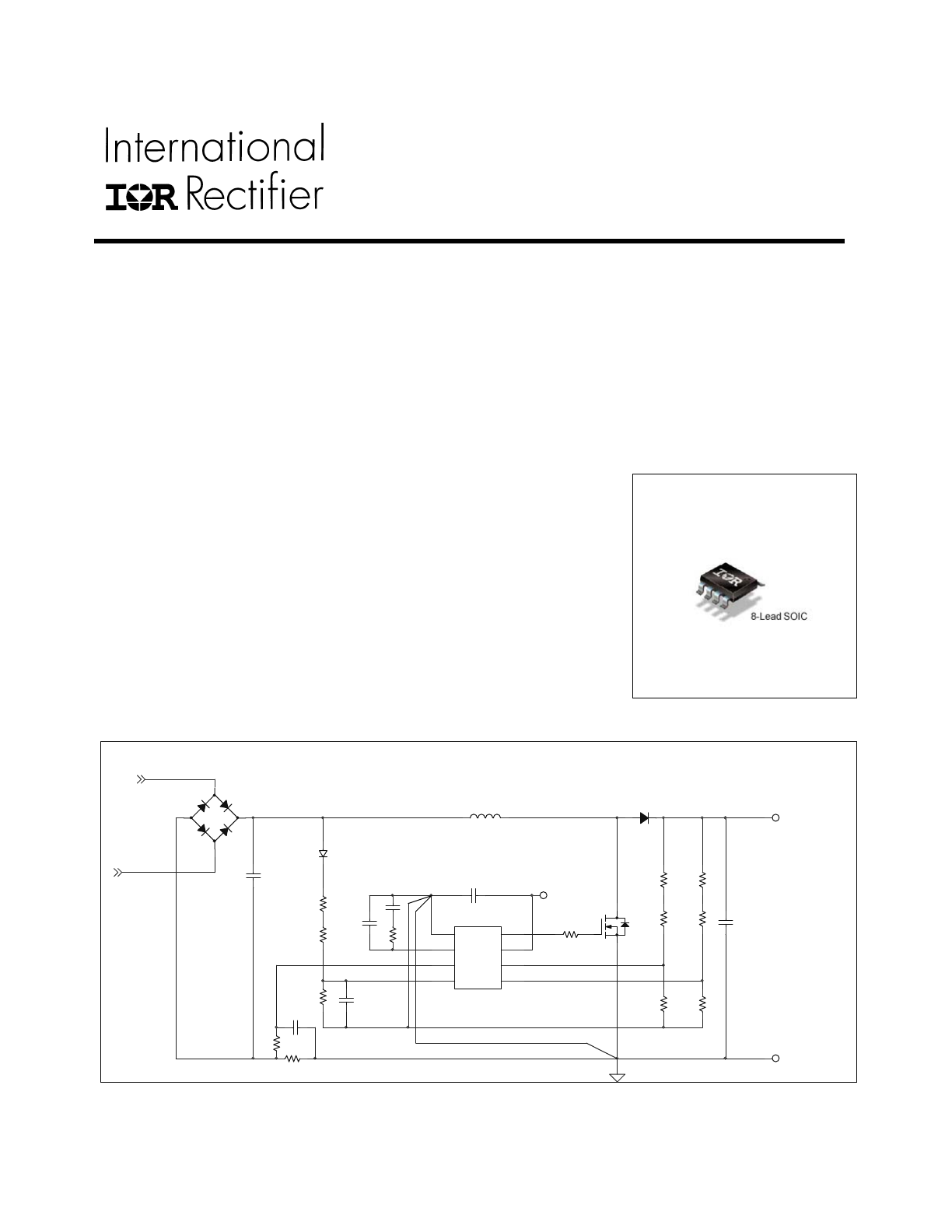
IR1153 Application Diagram
• PFC IC with IR proprietary “One Cycle Control”
• Continuous conduction mode boost type PFC
• Fixed 22.2kHz switching frequency
• Average current mode control
• Input line sensed brownout protection
• Output overvoltage protection
• Open loop protection
• Cycle by cycle peak current limit
• VCC under voltage lockout
• Programmable soft start
• Micropower startup
• User initiated micropower “Sleep Mode”
• 750mA peak gate drive
• Latch immunity and ESD protection
The μPFC IR1153 power factor correction IC, based on IR proprietary
"One Cycle Control" (OCC) technique, provides for high PF, low THD
and excellent DC Bus regulation while enabling drastic reduction in
component count, PCB area and design time as compared to traditional
solutions. The IC is designed to operate in continuous conduction mode
Boost PFC converters with average current mode control at a fixed
22.2kHz switching frequency. The IR1153 features include input-line
sensed brown-out protection, dedicated pin for over voltage protection,
cycle by cycle peak current limit, open loop protection, VCC UVLO, soft-
start and micropower startup current of less than 75µA. In addition, for
standby power requirements, the IC can be driven into a micropower
sleep mode by pulling the OVP/EN pin low where the current
consumption is less than 75uA. IR1153 is available in SO-8 package.
COM
1
BOP
4
VFB
6
VCC
7
GATE
8
ISNS
3
COMP
2
OVP/EN
5
ACIN1
ACIN2
IR1144
VOUT
RTN
VCC
-
+
IR1153
IR1153S
www.irf.com
2
© 2011 International Rectifier
Qualification Information
Industrial
Qualification Level
Comments: This family of ICs has passed JEDEC’s Industrial qualification.
IR’s Consumer qualification level is granted by extension of the higher
Industrial level.
Moisture Sensitivity Level
MSL2 260°C
(per IPC/JEDEC J-STD-020)
Machine Model
Class A
(per JEDEC standard JESD22-A115)
ESD
Human Body Model
Class 1A
(per EIA/JEDEC standard EIA/JESD22-A114)
IC Latch-Up Test
Class I, Level A
(per JESD78)
RoHS Compliant
Yes
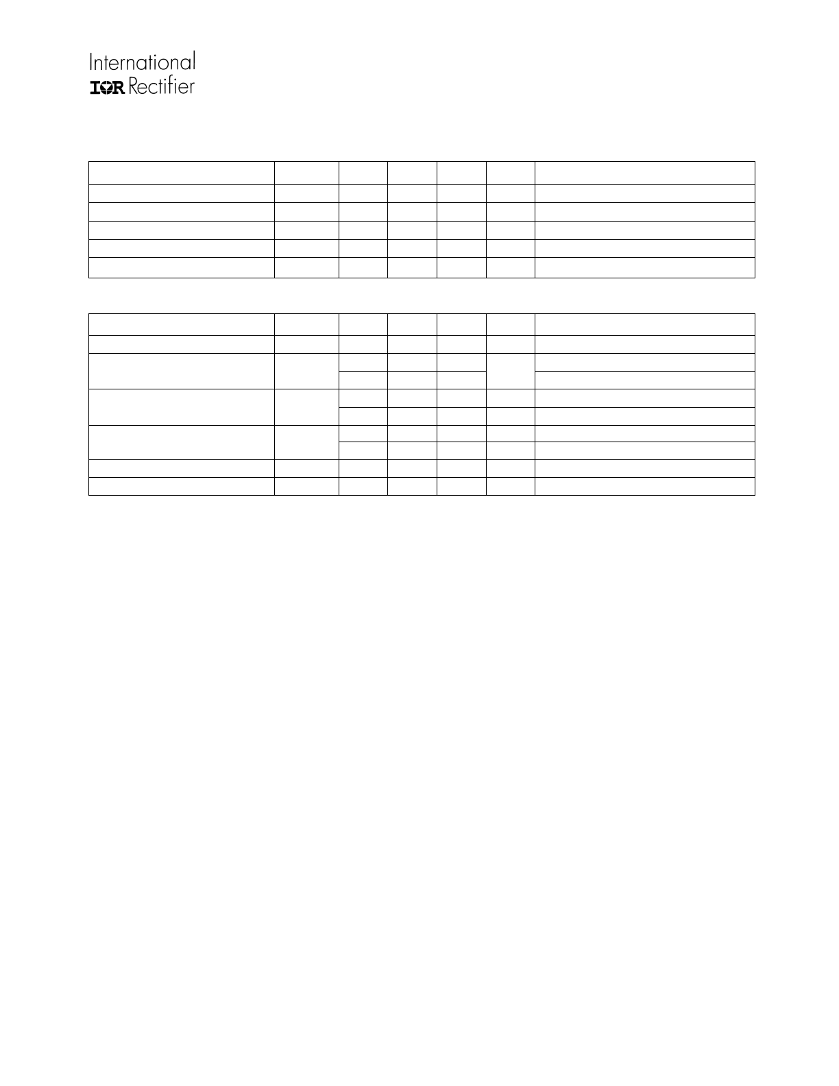
Absolute Maximum Ratings
Stresses beyond those listed under “Absolute Maximum Ratings” may cause permanent damage to the
device. These are stress ratings only and functional operation of the device at these conditions is not implied.
All voltages are absolute voltages referenced to COM. Thermal resistance and power dissipation are
measured under board mounted and still air conditions.
Parameters Symbol
Min.
Max.
Units Remarks
V
CC
Voltage
V
CC
-0.3
20
V
Not internally clamped
ISNS voltage
V
ISNS
-10 0.3 V
ISNS Current
I
ISNS
-2
2
mA
V
FB
voltage
V
FB
-0.3
6.5
V
V
OVP
voltage
V
OVP
-0.3 6.5 V
V
BOP
voltage
V
BOP
-0.3 9
V
COMP voltage
V
COMP
-0.3 6.5
V
Gate Voltage
V
GATE
-0.3
18
V
Junction Temperature Operating
Range T
J
-40 150 °C
Storage Temperature
T
S
-55 150 °C
Thermal Resistance
R
θJA
128
°C/W
SOIC-8
Package Power Dissipation
P
D
976
mW
T
AMB
=25°C SOIC-8
IR1153S
www.irf.com
3
© 2011 International Rectifier
Electrical Characteristics
The electrical characteristics involve the spread of values guaranteed within the specified supply voltage and
junction temperature range T
J
from – 25° C to 125°C. Typical values represent the median values, which are
related to 25°C. If not otherwise stated, a supply voltage of V
CC
=15V is assumed for test condition.
Supply Section
Parameters Symbol
Min.
Typ.
Max.
Units
Remarks
Supply Voltage Operating
Range
V
CC
14
17
V
V
CC
Turn On Threshold
V
CC ON
12.2 13.1 14 V
V
CC
Turn Off Threshold
(Under Voltage Lock Out)
V
CC UVLO
9.4 10.1 10.8 V
V
CC
Turn On/Off Hysteresis V
CC HYST
2.4 3 3.6 V
7
mA
C
LOAD
=1nF
8
mA
C
LOAD
=4.7nF
Operating Current
I
CC
3.5
5
mA
OVP Mode, Inactive gate
Start-up Current
I
CC START
26 75 µA
V
CC
=V
CC
ON
- 0.2V
Sleep current
I
SLEEP
26
75
µA
Pin
OVP/EN=V
SLEEP
-0.2V
Sleep Mode Threshold
V
SLEEP
0.5
0.8
V
Bias on OVP/EN pin
Oscillator Section
Parameters Symbol
Min.
Typ.
Max.
Units
Remarks
20.2 22.2 24.2
T
AMB
=25
°C
Fixed Oscillator Frequency
f
SW
18.3 25 kHz
-25
°C < T
AMB
< 125
°C
Maximum Duty Cycle
D
MAX
93
99 %
V
COMP
=5V
Minimum Duty Cycle
D
MIN
0
%
Pulse Skipping
Protection Section
Parameters Symbol
Min.
Typ.
Max.
Units
Remarks
Open Loop Protection
(OLP)Threshold
V
OLP
17 19 21
%
V
REF
Bias on VFB pin
Output Overvoltage
Protection (OVP)
Threshold
V
OVP
104 106 108
%
V
REF
Bias on OVP/EN pin
Output Overvoltage
Protection Reset Threshold
V
OVP(RST)
101 103 105
%
V
REF
Bias on OVP/EN pin
OVP Input Bias Current
I
OVP(Bias)
-0.2 µA
Brown-out Protection
(BOP) Threshold
V
BOP
0.66
0.76
0.86
V
Bias on BOP pin
Brown-out Protection
Enable Threshold
V
BOP(EN)
1.46
1.56
1.66
V
Bias on BOP pin
BOP Input Bias Current
I
BOP(Bias)
-0.2 µA
Peak Current Limit
Protection ISNS Voltage
Threshold (IPK LIMIT)
V
ISNS(PK)
-0.58 -0.51 -0.44
V
Bias on ISNS pin
IR1153S
www.irf.com
4
© 2011 International Rectifier
Internal Voltage Reference Section
Parameters Symbol
Min.
Typ.
Max.
Units
Remarks
Reference Voltage
V
REF
4.9 5 5.1 V
Regulation Voltage on VFB pin,
T
AMB
=25°C
Line Regulation
R
REG
10
20
mV
14V < V
CC
< 17V
Temp Stability
T
STAB
0.4
%
-25°C < T
AMB
< 125°C, Note 1
Total Variation
ΔV
TOT
4.83
5.12
V
Line & Temperature
Voltage Error Amplifier Section
Parameters Symbol
Min.
Typ.
Max.
Units
Remarks
Transconductance g
m
35
49 59 µS
30
44
58 T
AMB
=25°C
Source Current (Normal
Mode)
I
OVEA(SRC)
17 80
µA
-25°C < T
AMB
< 125°C
-58 -44 -30
T
AMB
=25°C
Sink Current (Normal Mode)
I
OVEA(SNK)
-80 -17
µA
-25°C < T
AMB
< 125°C
Soft Start Delay Time
(calculated)
t
SS
35 msec
R
GAIN
=8k
Ω, C
ZERO
=0.33
μF,
C
POLE
=2nF
V
COMP
Voltage (Fault)
V
COMP FLT
1
1.5
V
@100uA steady state
Effective V
COMP
voltage
V
COMP EFF
4.7
4.9
5.1
V
VFB Input Bias Current
I
FB(Bias)
-0.2
µA
Output Low Voltage
V
OL
0.25
V
Output High Voltage
V
OH
5
5.45 V
V
COMP
Start Voltage
V
COMP
START
210 325 435 mV
IR1153S
www.irf.com
5
© 2011 International Rectifier
Current Amplifier Section
Parameters Symbol
Min.
Typ.
Max.
Units
Remarks
DC Gain
g
DC
5.65
V/V
Corner Frequency
f
C
2
kHz
Average Current Mode, Note 1
Input Offset Voltage
V
IO
4
16
mV
Note 1
ISNS Input Bias Current
I
ISNS(Bias)
-57
-13 µA
Blanking Time
T
BLANK
170 320 470 ns
Gate Driver Section
Parameters Symbol
Min.
Typ.
Max.
Units
Remarks
Gate Low Voltage
V
GLO
0.8 V
I
GATE
= 200mA
13.1 14.1 15.1
V
CC
=17V, Internally Clamped
Gate High Voltage
V
GTH
9.5
V
V
CC
=11.5V
25
ns
C
LOAD
= 1nF, VCC=15V
Rise Time
t
r
60
ns
C
LOAD
= 4.7nF, VCC=15V
35
ns
C
LOAD
= 1nF, VCC=15V
Fall Time
t
f
65
ns
C
LOAD
= 4.7nF, VCC=15V
Output Peak Current
I
OPK
750
mA
C
LOAD
= 4.7nF, VCC=15V, Note 1
Gate Voltage at Fault
V
G fault
0.08
V
I
GATE
= 20mA
Note 1:
Guaranteed by design, but not tested in production
IR1153S
www.irf.com
6
© 2011 International Rectifier
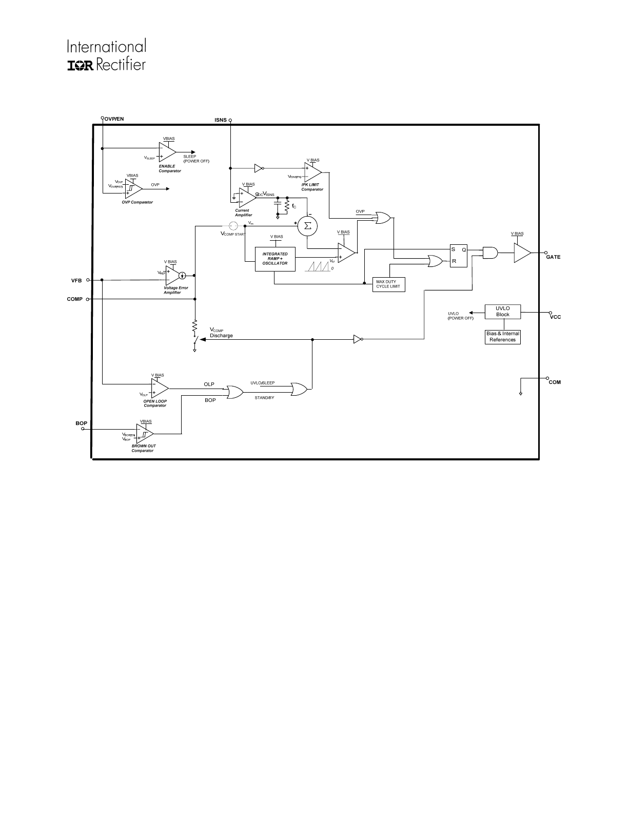
Block Diagram
IR1153S
www.irf.com
7
© 2011 International Rectifier
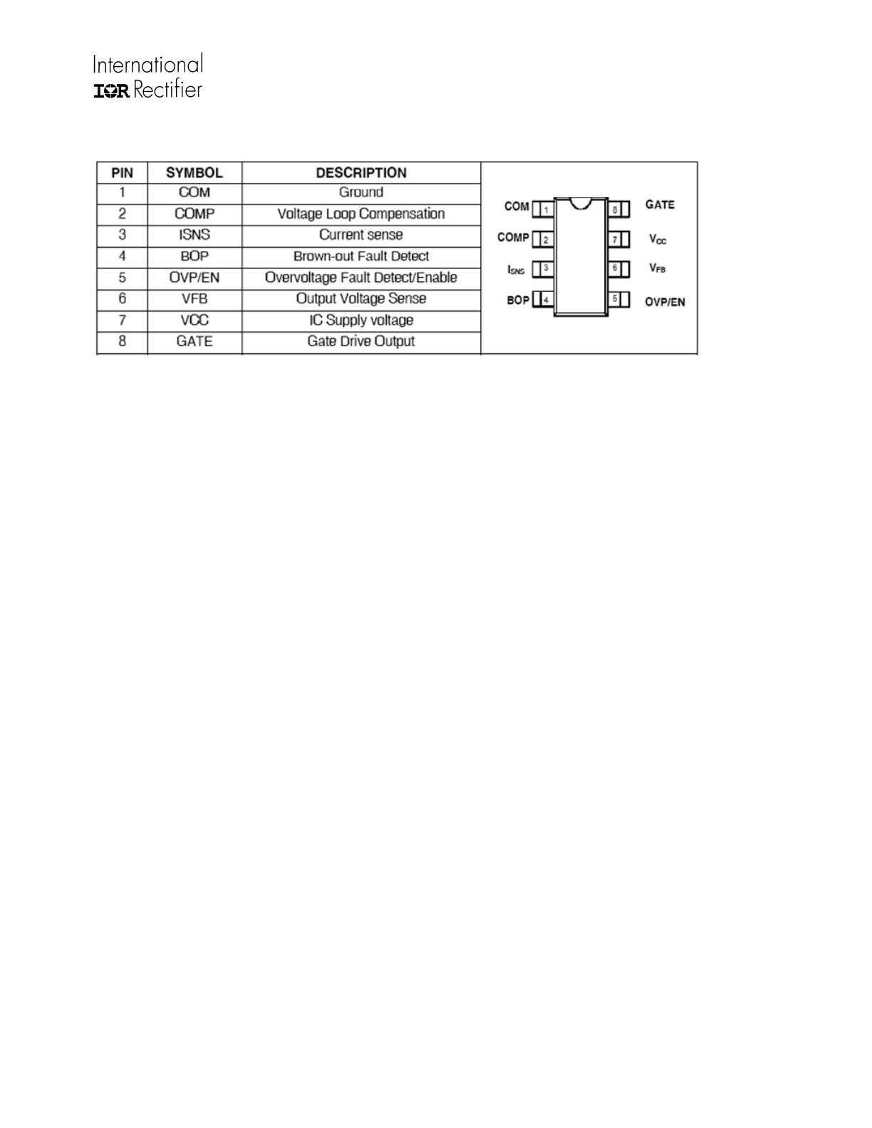
Lead Assignments & Definitions
IRS1144
IRS1144
IR1144S
IRS1144
IRS1144
IR1144S
IR1153

IR1153S
www.irf.com
8
© 2011 International Rectifier
IR1153 General Description
The μPFC IR1153 IC is intended for power factor
correction in continuous conduction mode Boost PFC
converters operating at fixed switching frequency with
average current mode control. The IC operates based
on IR's proprietary "One Cycle Control" (OCC) PFC
algorithm based on the concept of resettable
integrator.
Theory of Operation
The OCC algorithm based on the resettable integrator
concept works using two loops - a slow outer voltage
loop and a fast inner current loop. The outer voltage
loop monitors the VFB pin and generates an error
signal which controls the amplitude of the input current
admitted into the PFC converter. In this way, the outer
voltage loop maintains output voltage regulation. The
voltage loop bandwidth is kept low enough to not track
the 2xf
AC
ripple in the output voltage and thus
generates an almost DC error signal under steady
state conditions.
The inner current loop maintains the sinusoidal profile
of the input current and thus is responsible for power
factor correction. The information about the sinusoidal
variation in input voltage is inherently available in the
input line current (or boost inductor current). Thus
there is no need to sense the input voltage to
generate a current reference. The current loop
employs the boost inductor current information to
generate PWM signals with a proportional sinusoidal
variation. This controls the shape of the input current
to be proportional to and in phase with the input
voltage. Average current mode operation is envisaged
by filtering the switching frequency ripple from the
current sense signal using an appropriately sized on-
chip RC filter. This filter also contributes to the
bandwidth of the current control loop. Thus the filter
bandwidth has to be high enough to track the 120Hz
rectified, sinusoidal current waveform and also filter
out the switching frequency ripple in the inductor
current. In IR1153 this averaging function can
effectively filter high ripple current ratios (as high as
40% at maximum input current) to accommodate
designs with small boost inductances.
The IC determines the boost converter instantaneous
duty cycle based on the resettable integrator concept.
The required signals are the voltage feedback loop
error signal V
m
(which is the V
COMP
pin voltage minus a
DC offset of V
COMP,START
) and the current sense signal
V
ISNS
. The resettable integrator generates a cycle-by-
cycle, saw-tooth signal called the PWM Ramp which
has an amplitude V
m
and period 1/f
SW
hence a slope of
V
m*
f
SW
.
The current sense signal is amplified by the current
amplifier by a factor g
DC
and fed into the summing
node where it is subtracted from V
m
to generate the
summer voltage (= V
m
–g
DC
*V
ISNS
). The summer
voltage is compared with the PWM ramp by the
PWM comparator of the IC to determine the gate
drive duty cycle. The instantaneous duty is
mathematically given by:
D = (V
m
- g
DC
.V
ISNS
)/V
m
Assuming steady state condition where the voltage
feedback loop is well regulated (V
m
& V
OUT
are DC
signals) & hence instantaneous duty cycle follows
the boost-converter equation (D = 1 – V
IN
(t)/V
OUT
),
the control equation can be re-written as:
V
m
= g
DC
.V
ISNS
/(V
IN
(t)/V
OUT
)
Further, recognizing that V
ISNS
= I
L
(t).R
SNS
and re-
arranging yields:
g
DC
.I
L
(t).R
SNS
= V
m
V
IN
(t)/V
OUT
Since V
m
, V
OUT
& g
DC
are constant terms:
I
L
(t)
α V
IN
(t)
Thus the inductor current follows the input voltage
waveform & by definition power factor correction is
achieved.
Feature set
Fixed Frequency Operation
The IC is programmed to operate at a fixed
frequency of 22.2kHz (Typ). Internalization of the
oscillator offers excellent noise immunity even in
the noisy PFC environment while integration of the
oscillator into the OCC core of the IC eliminates
need for digital calibration circuits. Both these
factors render the gate drive jitter free thus
contributing to elimination of audible noise in PFC
magnetics.
IC Supply Circuit & Low start-up current
The IR1153 UVLO circuit maintains the IC in UVLO
mode during start-up if VCC pin voltage is less than
the VCC turn-on threshold, V
CC,ON
and current
consumption is less than 75uA. Should VCC pin
voltage should drop below V
CC,UVLO
during normal
operation, the IC is pushed back into UVLO mode
and VCC pin has to exceed V
CC,ON
again for normal
operation. There is no internal voltage clamping of
the VCC pin.
User initiated Micropower Sleep mode
The IC can be actively pushed into a micropower
Sleep Mode where current consumption is less
than 75uA by pulling OVP/EN pin below the Sleep
threshold, V
SLEEP
even while VCC is above V
CC,ON
.
This allows the user to disable PFC during
application stand-by situations in order to meet
stand-by regulations. Since V
SLEEP
is less than 1V,
even logic level signals can be employed.

IR1153S
www.irf.com
9
© 2011 International Rectifier
IR1153 General Description
Programmable Soft Start
The soft start process controls the rate of rise of the
voltage feedback loop error signal thus providing a
linear increase of the RMS input current that the
PFC converter will admit. The soft start time is
essentially controlled by voltage error amplifier
compensation components selected and is
therefore user programmable to some degree
based on desired voltage feedback loop crossover
frequency.
Gate Drive Capability
The gate drive output stage of the IC is a totem
pole driver with 750mA peak current drive
capability. The gate drive is internally clamped at
14.1V (Typ). Gate drive buffer circuits (especially
cost-effective base-followers) can be easily driven
with the GATE pin of the IC to suit any system
power level.
System Protection Features
IR1153 protection features include Brown-out
protection (BOP), Open-loop protection (OLP),
Overvoltage protection (OVP), Cycle-by-cycle peak
current limit (IPK LIMIT), Soft-current limit and VCC
under voltage lock-out (UVLO).
- BOP is based on direct input line sensing using a
resistor divider/RC filter network. If BOP pin falls
below the Brown-out protection threshold V
BOP
, a
Brown-out situation is immediately detected the
following response is executed - the gate drive
pulse is disabled, VCOMP is actively discharged
and IC is pushed into Stand-by Mode. The IC re-
enters normal operation only after BOP pin
exceeds V
BOP(EN)
. During start-up the IC is held in
Stand-by Mode until this pin exceeds V
BOP(EN)
.
- OLP is activated whenever the VFB pin voltage
falls below V
OLP
threshold. Once open loop is
detected the following response is immediately
executed - the gate drive is immediately disabled,
VCOMP is actively discharged and the IC is
pushed into Stand-by mode. There is no voltage
hysteresis associated with this feature. During
start-up the IC is held in Stand-by Mode until VFB
exceeds V
OLP
.
- The OVP pin is a dedicated pin for overvoltage
protection that safeguards the system even if
there is a break in the VFB feedback loop due to
resistor divider failure etc. An overvoltage fault is
triggered when OVP pin voltage exceeds the V
OVP
threshold of 106%VREF. The response of the IC
is to immediately terminate the gate drive output
and hold it in that state. The gate drive is re-
enabled only after OVP pin voltage drops below
V
OVP(RST)
threshold of 103% VREF. The exact
voltage level at which overvoltage protection is
triggered can be programmed by the user by
carefully designing the OVP pin resistor divider. It
is recommended NOT to set the OVP voltage
trigger limit less than 106% of DC bus voltage,
since this can endanger the situation where the
OVP reset limit will be less than the DC bus
voltage regulation point – in this condition the
voltage loop can become unstable.
- Soft-current limit is an output voltage fold-back
type protection feature encountered when the
PFC converter input current exceeds to a point
where the V
m
voltage saturates. As mentioned
earlier, the amplitude of input current is directly
proportional to V
m
, the error voltage of the
feedback loop. V
m
is clamped to a certain
maximum voltage inside the IC (given by
V
COMP,EFF
parameter in datasheet). If the input
current causes the V
m
voltage to saturate at its
maximum value, then any further increase in input
current will cause the duty cycle to droop which
immediately forces the V
OUT
voltage of the PFC
converter to fold-back. Since the highest current
is at the peak of the AC sinusoid, the droop in
duty cycle commences at the peak of the AC
sinusoid when the soft-current limit is
encountered. In most converters, the design of
the current sense resistor is performed based on
soft-current limit (i.e. V
m
saturation) and at the
system condition which demands highest input
current (minimum V
AC
& maximum P
OUT
).
- Cycle-by-cycle peak current limit protection
instantaneously turns-off the gate output
whenever the ISNS pin voltage exceeds V
ISNS(PK)
threshold in magnitude. The gate drive is held in
the low state as long as the overcurrent condition
persists. The gate drive is re-enabled when the
magnitude of ISNS pin voltage falls below the
V
ISNS(PK)
threshold. This protection feature
incorporates a leading edge blanking circuit to
improve noise immunity.

IR1153S
www.irf.com
10
© 2011 International Rectifier
IR1153 Pin Description
Pin COM:
This is ground potential pin of the IC.
All internal devices are referenced to this point.
Pin COMP:
External circuitry from this pin to
ground compensates the system voltage loop and
programs the soft start time. The COMP pin is
essentially the output of the voltage error
amplifier. The voltage loop error signal V
m
used in
the control algorithm is derived from V
COMP
(V
m
=V
COMP
–V
COMP,START
). V
COMP
is actively discharged
using an internal resistance to below V
COMP,START
threshold whenever the IC is pushed into Stand-
by mode (BOP or OLP condition) or UVLO/Sleep
mode. The gate drive output and logic functions of
the IC are inactive if VCOMP is less than
V
COMP,START
. Also during start-up, the VCOMP
voltage has to be less than V
COMP,START
in order to
commence operation (i.e. a pre-bias on VCOMP
will not allow IC to commence operation).
Pin ISNS:
ISNS pin is tied to the input of the
current sense amplifier of the IC. The voltage at
this pin, which provides the current sense
information to the IC, has to be a negative voltage
wrt the COM pin. Also since the IC is based on
average current mode, the entire inductor current
information is necessary. A current sense resistor,
located below system ground along the return
path to the bridge rectifier, is the preferred current
sensing method. ISNS pin is also the inverting
input to the cycle-by-cycle peak current limit
comparator. Whenever V
ISNS
exceeds V
ISNS(PK)
threshold in magnitude, the gate drive is
instantaneously disabled. Any external filtering of
the ISNS pin must be performed carefully in order
to ensure that the integrity of the current sense
signal is maintained for cycle-by-cycle peak
current limit protection.
Pin BOP (Brown-out Protection):
This pin is
used to sense the rectified AC input line voltage
through a resistor divider/capacitor network which
is in effect a voltage division and averaging
network, representing a scaled down signal of the
average rectified input voltage (average DC
voltage + 2xf
AC
ripple). During start-up the BOP
pin voltage has to exceed V
BOP(EN)
in order to
enable the IC to exit Stand-by mode and enter
normal operation. A Brown-out situation is
detected whenever the pin voltage falls below
V
BOP
and the IC is pushed into Stand-by mode.
Subsequently the pin has to exceed V
BOP(EN)
for
the IC to exit Stand-by and resume normal
operation.
Pin OVP/EN:
The OVP/EN pin is connected to the
non-inverting input of the OVP(OVP) overvoltage
comparator shown in the block diagram and thus
is used to detect output overvoltage situations.
The output voltage information is communicated
to the OVP pin using a resistive divider. This pin
also serves the second purpose of an ENABLE
pin. The OVP/EN pin can be used to activate the
IC into “micropower sleep” mode by pulling the
voltage on this pin below the V
SLEEP
threshold.
Pin VFB:
The converter output voltage is sensed
via a resistive divider and fed into this pin. VFB
pin is the inverting input of the output voltage error
amplifier. The non-inverting input of this amplifier
is connected to an internal 5V reference. The
impedance of the divider string must be low
enough that it does not introduce substantial error
due to the input bias currents of the amplifier, yet
high enough to minimize power dissipation.
Typical value of external divider total impedance
will be around 2MΩ. VFB pin is also the inverting
input to the Open Loop comparator. The IC is held
in Stand-by Mode whenever VFB pin voltage is
below V
OLP
threshold.
Pin VCC:
This is the supply voltage pin of the IC
and sense node for the undervoltage lock out
circuit. It is possible to turn off the IC by pulling
this pin below the minimum turn off threshold
voltage, V
CC(UVLO)
without damage to the IC. This
pin is not internally clamped.
Pin GATE:
This is the gate drive output of the IC.
It provides a drive current of ±0.75A peak with
matched rise and fall times. The gate drive output
of the IC is clamped at 14.1V(Typ).