
High‐Efficiency Variable Gate MOSFET Driver
CHL8515
December 6, 2011 | FINAL | V1.05
1
FEATURES
Ideal for Server Memory applications using +5V
Separate HVCC and LVCC capable of drive voltages
from 4.0 to 13.2V for optimal system efficiency
Adjustable thermal warning flag for phase‐by‐
phase thermal protection
Large drivers designed to drive 3nF in < 10ns with
any voltage from 5V to 12V (typ) supplied to the
HVCC and LVCC pins
Low‐side driver – 2A source/4A sink
High‐side driver – 2A source/2A sink
Transitions times & Propagation delays < 10ns
Integrated bootstrap diode
Capable of high switching frequencies from 200kHz
up to greater than 1MHz
Compatible with IR’s patented Active Tri‐Level
(ATL) PWM for fastest response to transient
overshoot
Non‐overlap and under voltage protection
Thermally enhanced 10‐pin DFN package
Lead free RoHS compliant package
Low Quiescent power to optimize efficiency
APPLICATIONS
Multiphase synchronous buck converter for Server
CPUs and DDR Memory VR solutions
High efficiency and compact VRM
Optimized for Sleep state S3 systems using +5VSB
Notebook Computer and Graphics VR solutions
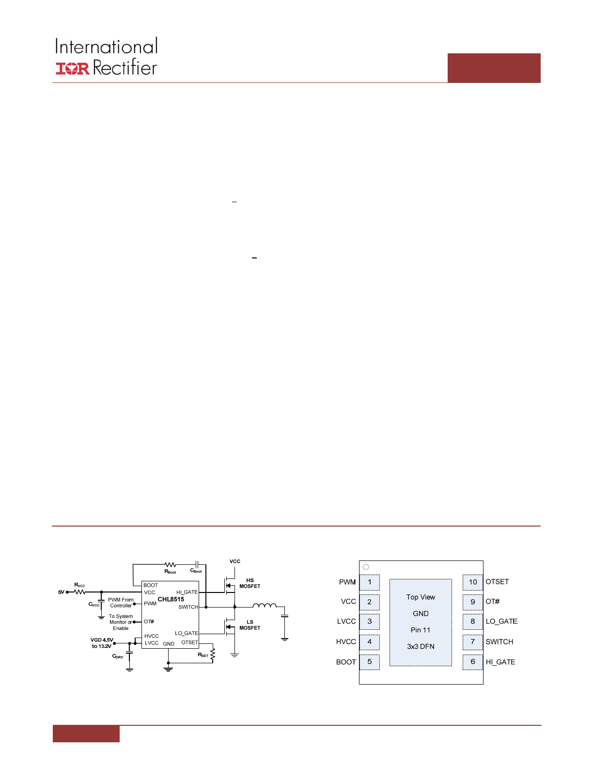
BASIC APPLICATION
Figure 1: CHL8515 Basic Application Circuit
DESCRIPTION
The CHL8515 MOSFET driver is a high‐efficiency gate driver
which can switch both high‐side and low‐side N‐channel
external MOSFETs in a synchronous buck converter. It is
intended for use with IR Digital PWM controllers to provide
a total voltage regulator (VR) solution for today’s advanced
computing applications.
The CHL8515 driver is capable of rapidly switching large
MOSFETs with low R
dson
and large input capacitance used
in high‐efficiency designs. It is uniquely designed to
operate from a 5V source, minimizing load current.
It also has separate HVCC and LVCC drive inputs, capable
of 4.0V to 13.2V operation. Used in conjunction with IR’s
Variable Gate Drive controller feature, or a 5V standby
source in sleep mode, maximum power stage efficiency
can be attained.
The CHL8515 has a unique circuit which maintains drive
strength to the external MOSFETs regardless of the drive
voltage, insuring fast switching even at 5V as the drive
voltage. The integrated boot diode reduces external
component count. The CHL8515 also features an adaptive
non‐overlap control for shoot‐through protection.
The CHL8515 is configured to drive both the high and
low‐side switches from the patented IR fast Active Tri‐Level
(ATL) PWM signal, which will optimize the turn off time of
individual phases, optimizing transient performance.
Phase‐by‐phase thermal protection can be set from 61C
to 150C with a simple resistor setting, and a thermal flag
can be used to implement a thermal warning or thermal
shutdown of the system by connecting OT# pins together
and to the system enable in multiphase applications.
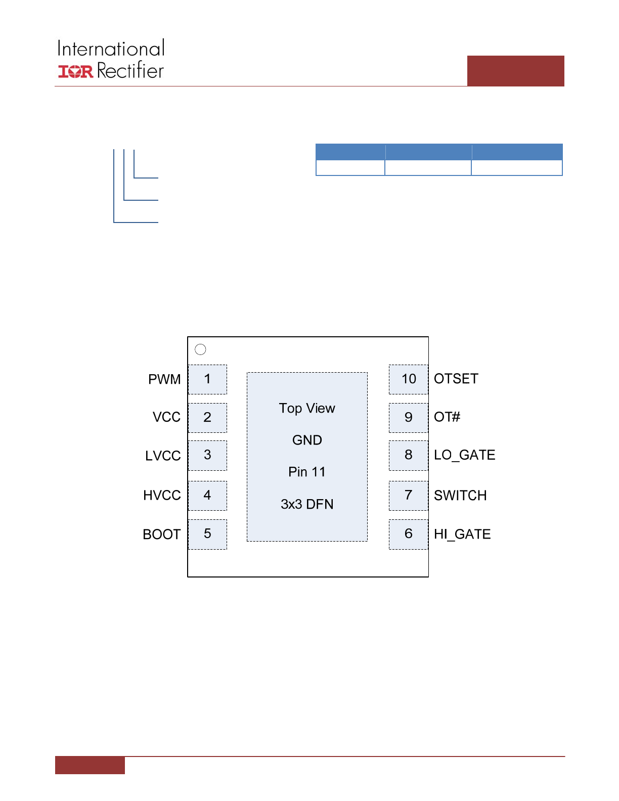
PIN DIAGRAM
Figure 2: CHL8515 Package Top View
High‐Efficiency Variable Gate MOSFET Driver
CHL8515
December 6, 2011 | FINAL | V1.05
2
ORDERING INFORMATION
CHL8515
Package
Tape & Reel Qty
Part Number
DFN
3000
CHL8515CRT
Figure 3: CHL8515 Pin Diagram Enlarged
T – Tape and Reel
R – Package Type (DFN)
C – Operating Temperature
(Commercial Standard)
High‐Efficiency Variable Gate MOSFET Driver
CHL8515
December 6, 2011 | FINAL | V1.05
3
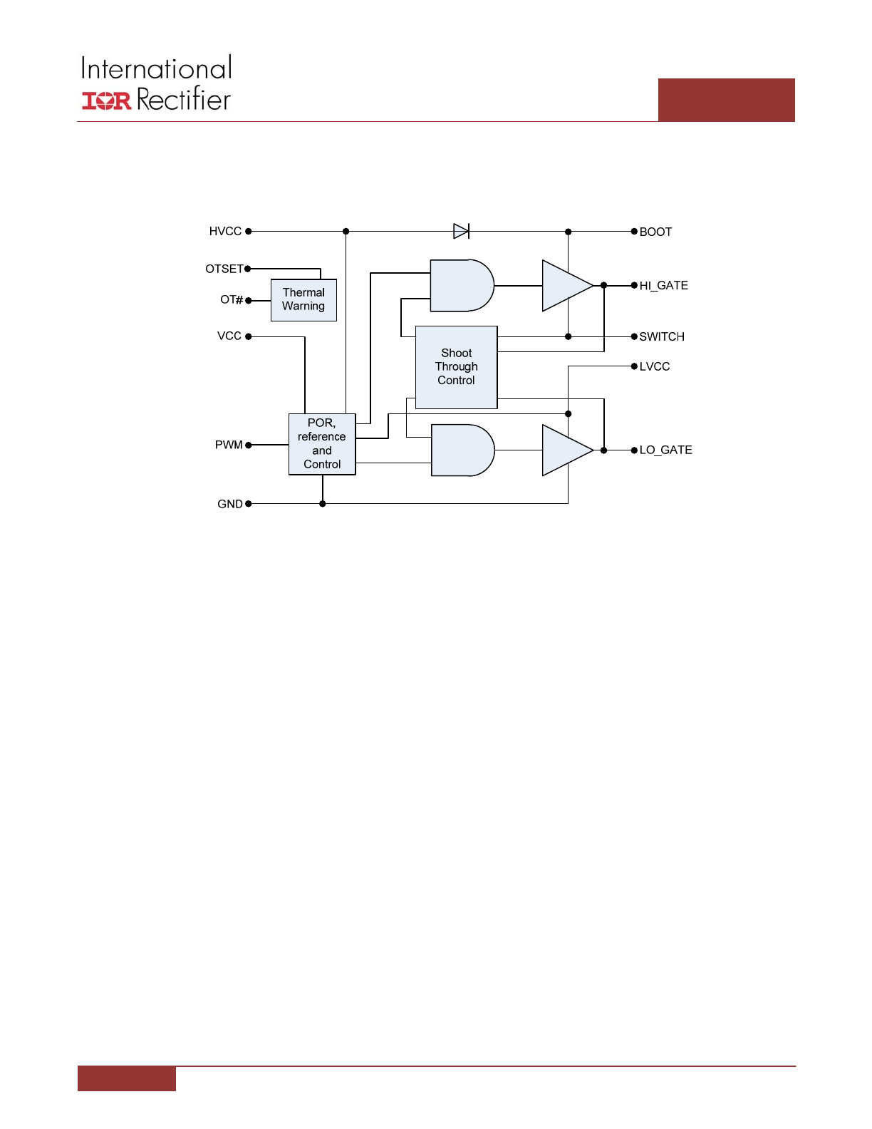
FUNCTIONAL BLOCK DIAGRAM
Figure 4: CHL8515 Simplified Functional Block Diagram
High‐Efficiency Variable Gate MOSFET Driver
CHL8515
December 6, 2011 | FINAL | V1.05
4
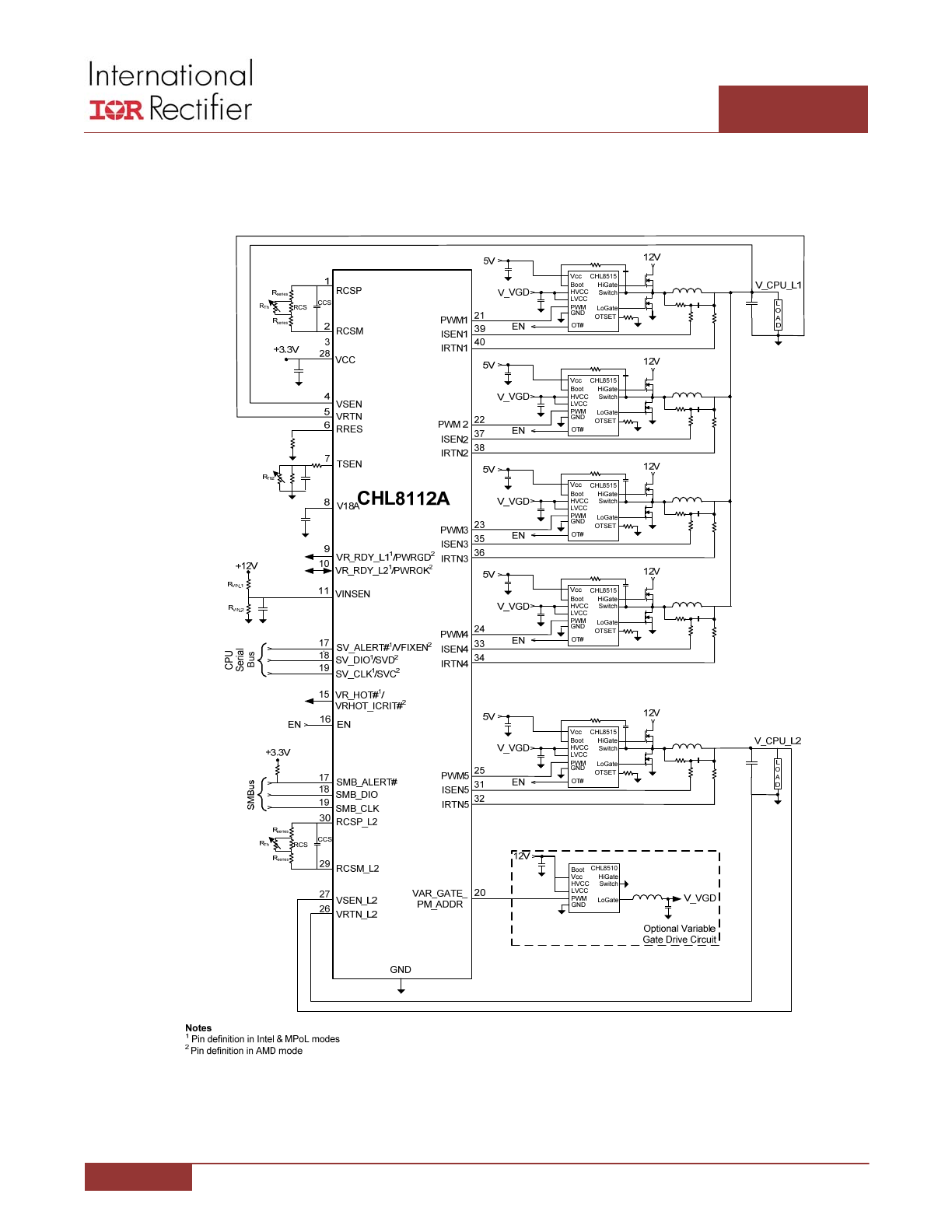
TYPICAL APPLICATION DIAGRAM
Figure 5: 4+1 CPU VR solution using CHL8515 MOSFET Drivers & CHL8112A Controller and CHL8510 Driver as VGD
High‐Efficiency Variable Gate MOSFET Driver
CHL8515
December 6, 2011 | FINAL | V1.05
5
PIN DESCRIPTIONS
PIN#
PIN NAME
PIN DESCRIPTION
1
PWM
The PWM signal is the control input for the driver from a 1.8V IR ATL‐based PWM signal. Connect this pin
to the PWM output of the controller.
2
VCC
Connect this pin to a +5V bias supply. Place a high quality low ESR ceramic capacitor from this pin to GND.
3
LVCC
Connect this pin to a separate supply voltage between 4.0V and 13.2V to vary the drive voltage on the
low‐side MOSFETs. Place a high quality low ESR ceramic capacitor from this pin to GND.
4
HVCC
Connect this pin to a separate supply between 4.0V and 13.2V to provide a lower gate drive voltage on the
high‐side MOSFETS. This is the anode of the internal bootstrap diode. Place a high quality low ESR ceramic
capacitor from this pin to GND.
5
BOOT
Floating bootstrap supply pin for the upper gate drive. Connect the bootstrap capacitor between this pin and
the SWITCH pin. The bootstrap capacitor provides the charge to turn on the upper MOSFET. See the Internal
Bootstrap Device section under DESCRIPTION for guidance in choosing the capacitor value.
6
HI_GATE
Upper gate drive output. Connect to gate of high‐side power N‐Channel MOSFET.
7
SWITCH
Connect this pin to the SOURCE of the upper MOSFET and the DRAIN of the lower MOSFET.
This pin provides a return path for the upper gate drive
8
LO_GATE
Lower gate drive output. Connect to gate of the low‐side power N‐Channel MOSFET.
9
OT#
Open drain active low signal indicating that the temperature of the Driver (very close to Phase temperature)
has exceeded the value set by the OTSET pin. Connect to system controller or to system Enable to create a
thermal shutdown.
10
OTSET
Use a 1% resistor to ground to set the Over Temperature set point from 61C to 150C.
Leave open to use default setting of 150C.
PAD (11)
GND
Bias and reference ground. All signals are referenced to this node. It is also the power ground return
of the driver.
High‐Efficiency Variable Gate MOSFET Driver
CHL8515
December 6, 2011 | FINAL | V1.05
6
ABSOLUTE MAXIMUM RATINGS
VCC
‐0.3V to +7.0V
LVCC, HVCC
‐0.3V to +15.0V
PWM, OTSET, OT#
‐0.3V to +7.0V
BOOT‐GND, BOOT‐SWITCH
‐0.3V to +35.0V, ‐0.3V to +HVCC
LO_GATE
‐0.3V to LVCC + 0.3V, <200ns: ‐5V to LVCC + 0.3V
HI_GATE
SWITCH – 0.3V to VBOOT + 0.3V, <20ns: SWITCH –5V to VBOOT + 0.3V
SWITCH
‐0.3V to +35.0V, <200ns, ‐8V
ESD
HBM 250V JEDEC Standard
Thermal Information
Thermal Resistance (θ
JC
)
3°C/W
Thermal Resistance (θ
JA
)
1
45°C/W
Maximum Operating Junction Temperature
150°C
Maximum Storage Temperature Range
‐65°C to 150°C
Maximum Lead Temperature (Soldering 10s)
300°C
Note: 1. θ
JA
is measured with the component mounted on a high effective thermal conductivity test board in free air.
Stresses beyond those listed under “Absolute Maximum Ratings” may cause permanent damage to the device. These are stress ratings
only and functional operation of the device at these or any other conditions beyond those indicated in the operational sections of the
specifications are not implied.
High‐Efficiency Variable Gate MOSFET Driver
CHL8515
December 6, 2011 | FINAL | V1.05
7
ELECTRICAL SPECIFICATIONS
RECOMMENDED OPERATING CONDITIONS FOR RELIABLE OPERATION WITH MARGIN
Recommended Operating Ambient Temperature Range
‐40°C to 85°C
Recommended Maximum Operating Junction Temperature
125°C
Supply Voltage Range
+5V ± 10%
HVCC, LVCC
+4.0V to +13.2V
The electrical characteristics table lists the spread of values guaranteed within the recommended operating conditions.
Typical values represent the median values, which are related to 25°C, unless otherwise specified. VCC = 5.0V, HVCC = 7.0V,
LVCC = 5.0V.
ELECTRICAL CHARACTERISTICS
PARAMETER
SYMBOL
CONDITIONS
MIN
TYP
MAX
UNIT
Supply
Idle Supply Bias Current
I
VCC +
I
VDRV
PWM input tri‐stated
‐
2.3
‐
mA
Active Supply Bias Current
I
VCC
VCC = 5V
2.7
3.1
3.5
mA
VCC Rising Threshold for POR
3.5
3.7
3.9
V
VCC Falling Threshold for POR
3.2
3.4
3.6
V
OTSET, OT#
Temperature Setpoint Open
OT
Rset = Open
‐
150
‐
°C
Temperature Setpoint Resistor
OT
Rset = 100kΩ
‐
125
‐
°C
Temperature Hysteresis
OT_HYST
‐
‐20
‐
°C
Temperature Flag Sink Current
OT# Sink
‐
1.5
‐
mA
Temperature Flag Sink Voltage
OT#
‐
0.8
‐
V
PWM Input IR ATL Mode
PWM Input High Threshold
V
IH(C_PWM)
‐
1.0
‐
V
PWM Input Low Threshold
V
IL(C_PWM)
‐
0.8
‐
V
PWM Input Tri‐level High Threshold
V
TL(C_PWM)
‐
2.5
‐‐
V
PWM Input Tri‐level Low Threshold
V
TH(C_PWM)
‐
2.3
‐
V
PWM Input Current Low
I
C_PWM
V
PWM
= 0V
‐
1.0
‐
mA
PWM Input Current High
V
PWM
= 1.8V
‐
1.0
‐
mA
High‐Side Gate Driver
Transition Time – Rise
t
R(HS)
3nF Load, 10% – 90%
‐
10
‐
ns
Transition Time – Fall
t
F(HS)
3nF Load, 10% – 90%
‐
8
‐
ns
Propagation Delay – Turn‐on
t
PDH(HS)
3nF Load, Adaptive
‐
19
‐
ns
Propagation Delay – Turn‐off
t
PDL(HS)
3nF Load
‐
20
‐
ns
Propagation Delay – Exit Tri‐state
t
PDTS(HS_en)
3nF Load
‐
35
‐
ns
Propagation Delay – Enter Tri‐state
t
PDTS(HS_dis)
3nF Load
‐
20
‐
ns
High‐Efficiency Variable Gate MOSFET Driver
CHL8515
December 6, 2011 | FINAL | V1.05
8
PARAMETER
SYMBOL
CONDITIONS
MIN
TYP
MAX
UNIT
Source Current
I
HS_SOURCE
3nF Load
‐
2
‐
A
Output Impedance Sourcing
R
HS_SOURCE
Sink Current at 100mA
‐
1.4
‐
Ω
Sink Current
I
HS_SINK
3nF Load
‐
2
‐
A
Output Impedance – Sinking
R
HS_SINK
Sink Current at 100mA
‐
0.7
‐
Ω
Low‐Side Gate Driver
Transition Time – Rise
t
F(LS)
3nF Load, 10% – 90%
‐
10
‐
ns
Transition Time – Fall
t
R(LS)
3nF Load, 10% – 90%
‐
7
‐
ns
Propagation Delay – Turn‐on
t
PDH(LS)
3nF Load, Adaptive
‐
9
‐
ns
Propagation Delay – Turn‐off
t
PDL(LS)
3nF Load
‐
25
‐
ns
Propagation Delay – Exit Tri‐state
t
PDTS(LS_en)
3nF Load
‐
36
‐
ns
Propagation Delay – Enter Tri‐state
t
PDTS(LS_dis)
3nF Load
‐
22
‐
ns
Source Current
I
LS_SOURCE
3nF Load
‐
2
‐
A
Output Impedance Sourcing
R
LS_SOURCE
Sink Current at 100mA
‐
1.5
‐
Ω
Sink Current
I
LS_SINK
3nF Load
‐
4
‐
A
Output Impedance – Sinking
R
LS_SINK
Sink Current at 100mA
‐
0.4
‐
Ω
Note:
1
Guaranteed by design
High‐Efficiency Variable Gate MOSFET Driver
CHL8515
December 6, 2011 | FINAL | V1.05
9
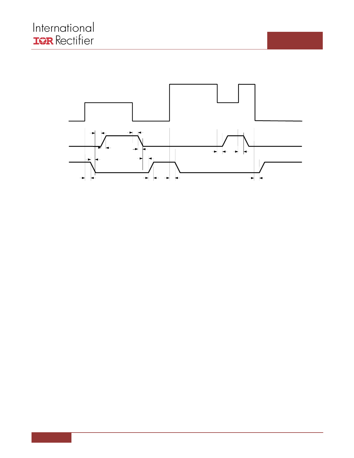
TIMING DIAGRAM
Figure 6: IR Active Tri‐Level (ATL) mode PWM, HI_GATE and LO_GATE signals
Normal PWM operation
Active Tri-level (ATL) PWM operation
HI_GATE
LO_GATE
PWM
R(HS)
PDTS(HS_en)
t
PDL(HS)
t
t
F(HS)
t
F(
LS)
t
R(LS)
t
PDL(LS)
t
PDH(LS)
t
PDTS(LS_dis)
t
t
PDL(HS)
t
PDTS(HS_dis)
t
PDTS(LS_en)

High‐Efficiency Variable Gate MOSFET Driver
CHL8515
December 6, 2011 | FINAL | V1.05
10
GENERAL DESCRIPTION
The CHL8515 is a high efficiency, fast MOSFET driver with
large source and sink current capability. It can reliably
drive the external high‐ and low‐side N‐channel MOSFETs
with large input capacitance at switching frequencies up to
1MHz. The patented IR Active Tri‐Level (ATL) feature allows
complete control over enable and disable of both MOSFETs
using the PWM input signal from the controller. The timing
and voltage levels of ATL are shown in Figure 6.
During normal operation the PWM transitions between
low and high voltage levels to drive the low‐ and high‐side
MOSFETs. The PWM signal falling edge transition to a low
voltage threshold initiates the high‐side driver turn off
after a short propagation delay, t
PDL(HS)
. The dead time
control circuit monitors the HI_GATE and switch voltages
to ensure the high‐side MOSFET is turned off before the
LO_GATE voltage is allowed to rise to turn on the low‐side
MOSFET.
The PWM rising edge transition through the high‐side turn
on threshold, initiates the turn off of the low‐side MOSFET
after a small propagation delay, t
PDL(LS)
. The adaptive
dead time circuit provides the appropriate dead time by
determining if the falling LO_GATE voltage threshold has
been crossed before allowing the HI_GATE voltage to rise
and turn on the high‐side MOSFET, t
PDH(HS)
.
.