
* Qualification standards can be found on IR’s web site www.irf.com
© 2009 International Rectifier
July 28
th
, 2010
Automotive Grade
AUIRS21811S
HIGH AND LOW SIDE DRIVER
Features
• Floating channel designed for bootstrap operation
• Fully operational to +600 V
• Tolerant to negative transient voltage, dV/dt
immune
• Gate drive supply range from 10V to 20V
• Undervoltage lockout for both channels
• 3.3V and 5V input logic compatible
• Matched propagation delay for both channels
• Lower di/dt gate driver for better noise immunity
• Output
source/sink current capability of 1.9A/2.3A
typical
• Leadfree, RoHS compliant
• Automotive qualified*
Typical Applications
• Piezo
injection
• Electric Power Steering
• Fan
and
compressor
• Starter/alternator
Product Summary
Topology
High and Low Side Driver
V
OFFSET
≤ 600V
V
OUT
10V – 20V
I
o+
& I
o-
(typical)
1.9A & 2.3A
t
on
& t
off
(typical)
135ns
Package Options
8 - Lead SOIC
AUIRS21811S
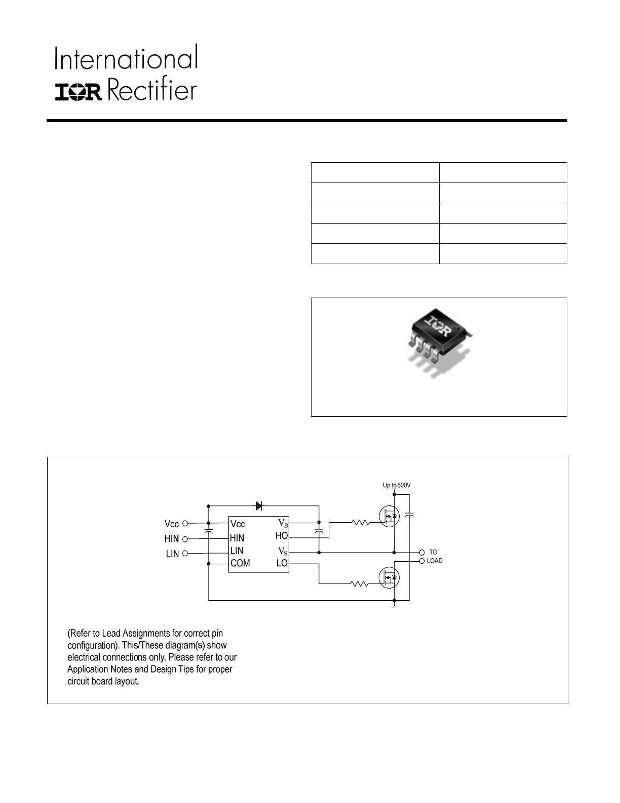
Typical Connection Diagram
AUIRS21811S
AUIRS21811S
www.irf.com
© 2009 International Rectifier
2
Table of Contents
Page
Typical Connection Diagram
1
Description/Feature Comparison
3
Qualification Information
4
Absolute Maximum Ratings
5
Recommended Operating Conditions
5
Dynamic Electrical Characteristics
6
Static Electrical Characteristics
6
Functional Block Diagram
7
Input/Output Pin Equivalent Circuit Diagram
8
Lead Definitions
9
Lead Assignments
9
Application Information and Additional Details
10
Parameter Temperature Trends
11-13
Package Details
14
Tape and Reel Details
15
Part Marking Information
16
Ordering Information
17
Important Notice
18
AUIRS21811S
www.irf.com
© 2009 International Rectifier
3
Description
The AUIRS21811S is a high voltage, high speed power MOSFET and IGBT driver with independent high and
low side referenced output channels. Proprietary HVIC and latch immune CMOS technologies enable
ruggedized monolithic construction. The logic input is compatible with standard CMOS or LSTTL output,
down to 3.3 V logic. The output drivers feature a high pulse current buffer stage. The floating channel can be
used to drive an N-channel power MOSFET or IGBT in the high-side configuration which operates up to
600V.
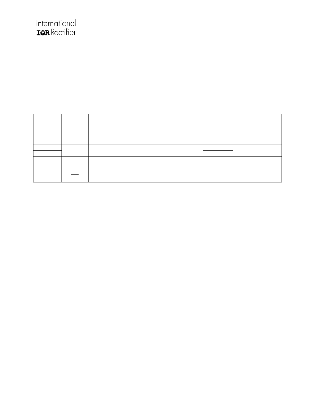
Feature Comparison: AUIRS21811/AUIRS2181/AUIRS2183/AUIRS2184
Part
Input
Logic
Cross-
Conduction
Prevention
logic
Dead-Time
Ground
Pins
Ton/Toff
(typical)
21811 HIN/LIN
No
none
COM 135/135
ns
2181 COM
21814
HIN/LIN
No
none
V
SS
/COM
160/200 ns
2183 Internal
500ns
COM
21834
HIN/LIN
Yes
Programmable 0.4 – 5 us
V
SS
/COM
180/220 ns
2184 Internal
500ns
COM
21844
IN/SD
Yes
Programmable 0.4 – 5 us
V
SS
/COM
600/230 ns
AUIRS21811S
www.irf.com
© 2009 International Rectifier
4
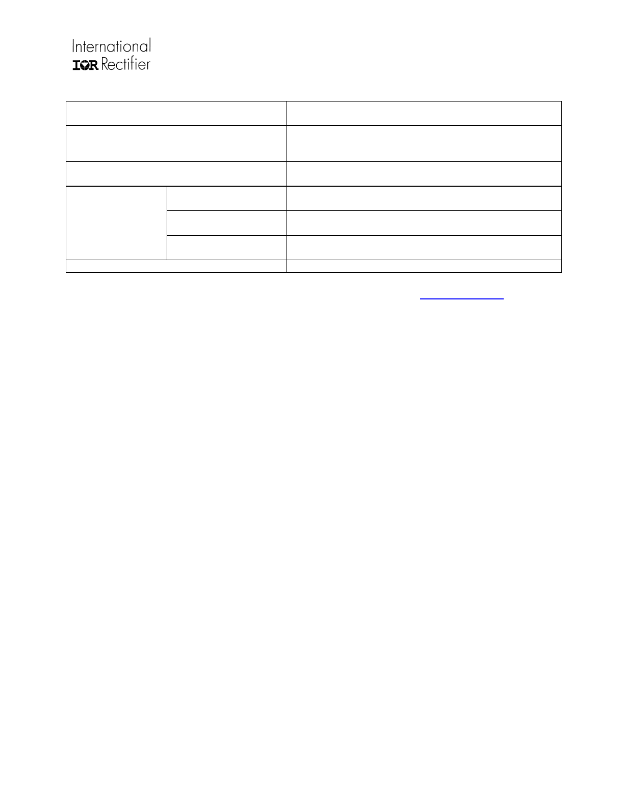
Qualification Information
†
Qualification Level
Automotive
(per AEC-Q100††)
Comments: This family of ICs has passed an Automotive
qualification. IR’s Industrial and Consumer qualification
level is granted by extension of the higher Automotive level.
Moisture Sensitivity Level
MSL3
†††
260°C
(per IPC/JEDEC J-STD-020)
Machine Model
Class M3 (Pass +/-250V)
(per AEC-Q100-003)
Human Body Model
Class H2 (Pass +/-2500V)
(per AEC-Q100-002)
ESD
Charged Device Model
Class C5 (Pass +/-1250V)
(per AEC-Q100-011)
RoHS Compliant
Yes
†
Qualification standards can be found at International Rectifier’s web site
http://www.irf.com/
†† Exceptions to AEC-Q100 requirements are noted in the qualification report.
††† Higher MSL ratings may be available for the specific package types listed here. Please contact your
International Rectifier sales representative for further information.
AUIRS21811S
www.irf.com
© 2009 International Rectifier
5
Absolute Maximum Ratings
Absolute Maximum Ratings indicate sustained limits beyond which damage to the device may occur. All
voltage parameters are absolute voltages referenced to COM lead. Stresses beyond those listed under "
Absolute Maximum Ratings" may cause permanent damage to the device. These are stress ratings only; and
functional operation of the device at these or any other condition beyond those indicated in the
“Recommended Operating Conditions” is not implied. Exposure to absolute-maximum-rated conditions for
extended periods may affect device reliability. The thermal resistance and power dissipation ratings are
measured under board mounted and still air conditions. Ambient temperature (T
A
) is 25°C, unless otherwise
specified.
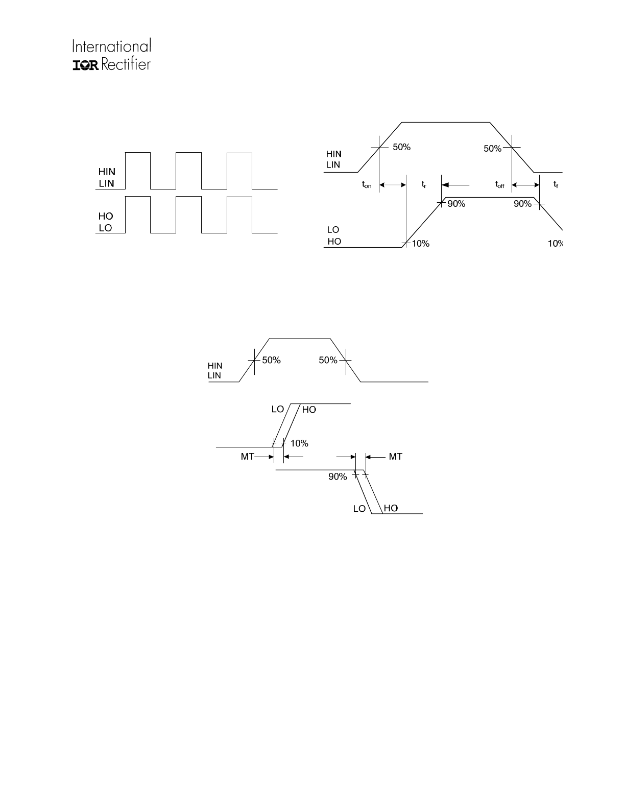
Recommended Operating Conditions
The Input/Output logic timing diagram is shown in Figure 1. For proper operation the device should be used
within the recommended conditions. V
S
and offset rating are tested with all supplies biased at 15V
differential.
† Logic operational for V
S
of -5V to +600V. Logic state held for V
S
of -5V to –V
BS
. (Please refer to Figure 4
for more details).
Symbol Definition
Min
Max
Units
V
B
High side floating absolute voltage
-0.3
620
V
S
High side floating supply offset voltage
V
B
- 25
V
B
+ 0.3
V
HO
High side floating output voltage
V
S
- 0.3
V
B
+ 0.3
V
CC
Low side and logic fixed supply voltage
-0.3
20
V
LO
Low side output voltage
-0.3
V
CC
+ 0.3
V
IN
Logic input voltage (HIN & LIN)
COM - 0.3 V
CC
+ 0.3
V
dV
S
/dt
Allowable offset supply voltage transient
—
50
V/ns
P
D
Package power dissipation @ TA ≤ 25°C
—
0.625
W
Rth
JA
Thermal resistance, junction to ambient
—
200
°C/W
T
J
Junction temperature
—
150
T
S
Storage
temperature
-50 150
T
L
Lead temperature (soldering, 10 seconds)
—
300
°C
Symbol Definition
Min
Max
Units
V
B
High side floating supply absolute voltage
V
S
+ 10
V
S
+ 20
V
S
High side floating supply offset voltage
†
600
V
HO
High side floating output voltage
V
S
V
B
V
CC
Low side and logic fixed supply voltage
10
20
V
LO
Low side output voltage
0
V
CC
V
IN
Logic input voltage (HIN & LIN)
COM
V
CC
V
T
A
Ambient temperature
-40
125
°C
AUIRS21811S
www.irf.com
© 2009 International Rectifier
6
Dynamic Electrical Characteristics
Unless otherwise noted, these specifications apply for an operating junction temperature range of -40°C ≤ Tj
≤ 125°C with bias conditions of V
CC
= V
BS
= 15V, V
S
= COM, C
L
= 1000pF.
Symbol Definition
Min Typ Max
Units
Test
Conditions
t
on
Turn-on propagation delay
— 135 230
V
S
= 0V
t
off
Turn-off propagation delay
— 135 230
V
S
= 0V or 600V
MT
Delay matching, HO & LO turn-on/off
—
—
35
t
r
Turn-on
rise
time
—
—
60
V
S
= 0V
t
f
Turn-off fall time
—
—
35
ns
V
S
= 0V
Static Electrical Characteristics
Unless otherwise noted, these specifications apply for an operating junction temperature range of -40°C ≤ Tj
≤ 125°C with bias conditions of V
CC
= V
BS
= 15V and V
S
= COM. The V
IN
and I
IN
parameters are referenced to
V
SS
/COM and are applicable to the respective input leads: HIN and LIN. The V
O
and I
O
parameters are
referenced to V
S
/COM and are applicable to the respective output leads: HO and LO.
(†) Guaranteed by design
(††) I
O+
and I
O-
decrease with rising temperature
Symbol Definition
Min Typ Max
Units
Test
Conditions
V
IH
Logic “1” input voltage
2.5
—
—
V
IL
Logic “0” input voltage
— — 0.8
V
CC
= 10V to 20V
V
OH
High level output voltage, V
BIAS
-
V
O
—
—
1.4
I
O
= 0mA
V
OL
Low level output voltage, V
O
—
—
0.2
V
I
O
= 20mA
I
LK
Offset supply leakage current
— —
50
V
B
=
V
S
= 600V
I
QBS
Quiescent
V
BS
supply current
25
80 200
I
QCC
Quiescent
V
CC
supply current
55 130 260
V
IN
= 0V or 5V
I
IN+
Logic “1” input bias current
— 25
60
V
IN
= 5V
I
IN-
Logic “0” input bias current
— — 1.0
µA
V
IN
= 0V
V
CCUV+
V
BSUV+
V
CC
and V
BS
supply undervoltage positive
going threshold
8.0 8.9
9.8
V
CCUV-
V
BSUV-
V
CC
and V
BS
supply undervoltage negative
going threshold
7.4 8.2
9.0
V
CCUVH
V
BSUVH
V
CC
and V
BS
supply undervoltage Hysteresis
0.3 0.7
—
V
I
O25+
(†)
Output high short circuit pulsed current
1.4 1.9
—
V
O
= 0V,
PW ≤ 10us,
T
J
= 25°C
I
O25-
(†)
Output low short circuit pulsed current
1.8 2.3
—
V
O
= 15V,
PW ≤ 10us,
T
J
= 25°C
I
O+
(†)
(††)
Output high short circuit pulsed current
1.2
—
—
V
O
= 0V,
PW ≤ 10us
I
O-
(†)
(††)
Output low short circuit pulsed current
1.5
—
—
A
V
O
= 15V,
PW ≤ 10us
AUIRS21811S
www.irf.com
© 2009 International Rectifier
7
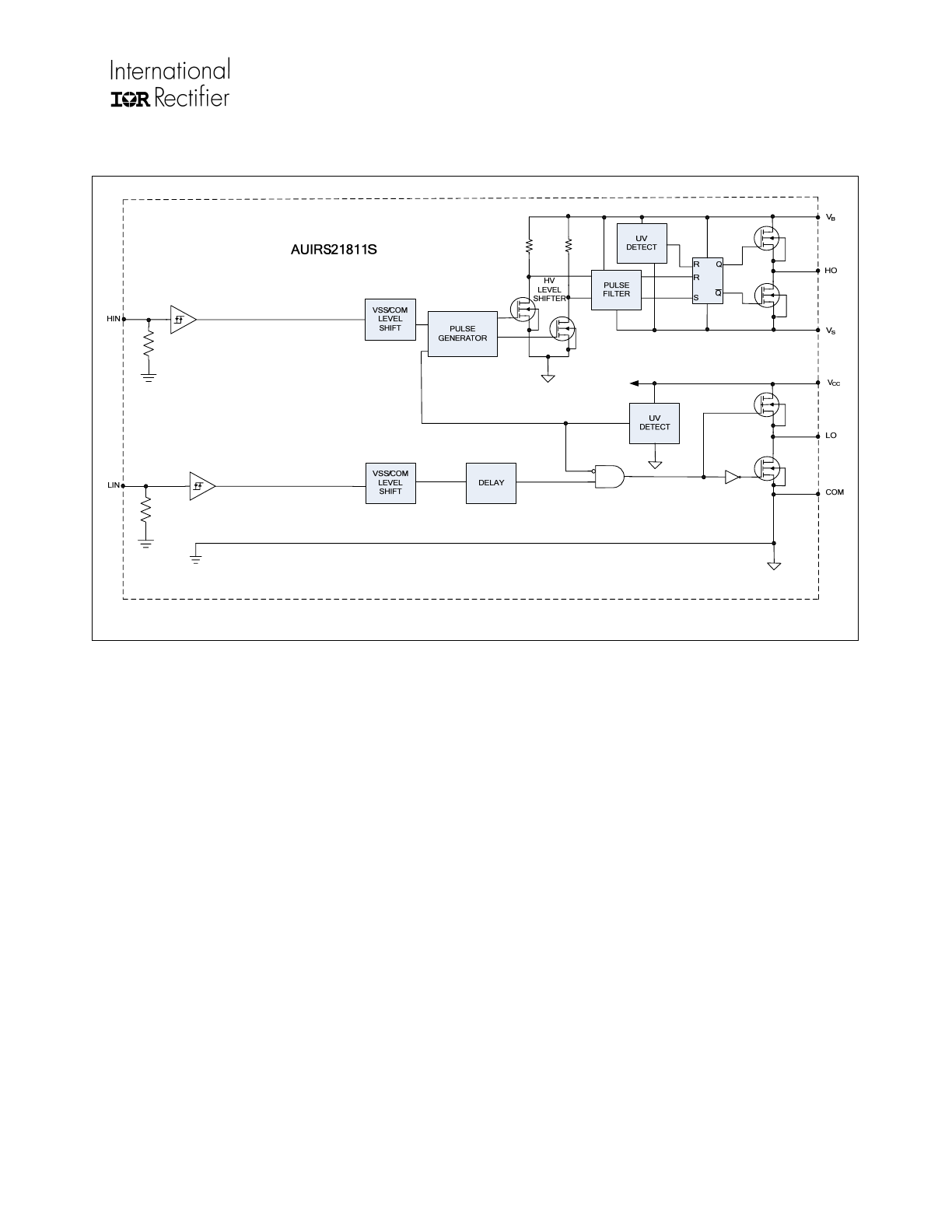
Functional Block Diagrams
AUIRS21811S
www.irf.com
© 2009 International Rectifier
8
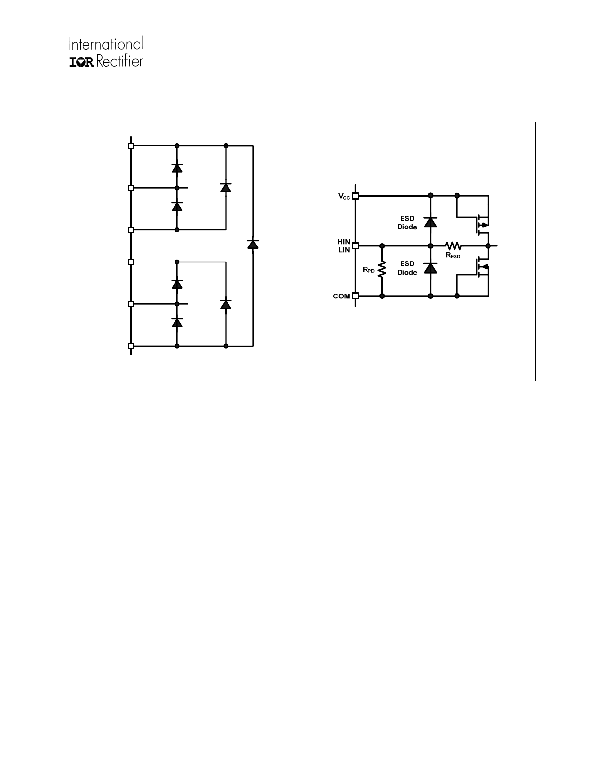
Input/Output Pin Equivalent Circuit
Diagrams
V
CC
COM/V
SS
LO
ESD
Diode
ESD
Diode
V
B
V
S
HO
ESD
Diode
ESD
Diode
20V
20V
600V
AUIRS21811S
www.irf.com
© 2009 International Rectifier
9
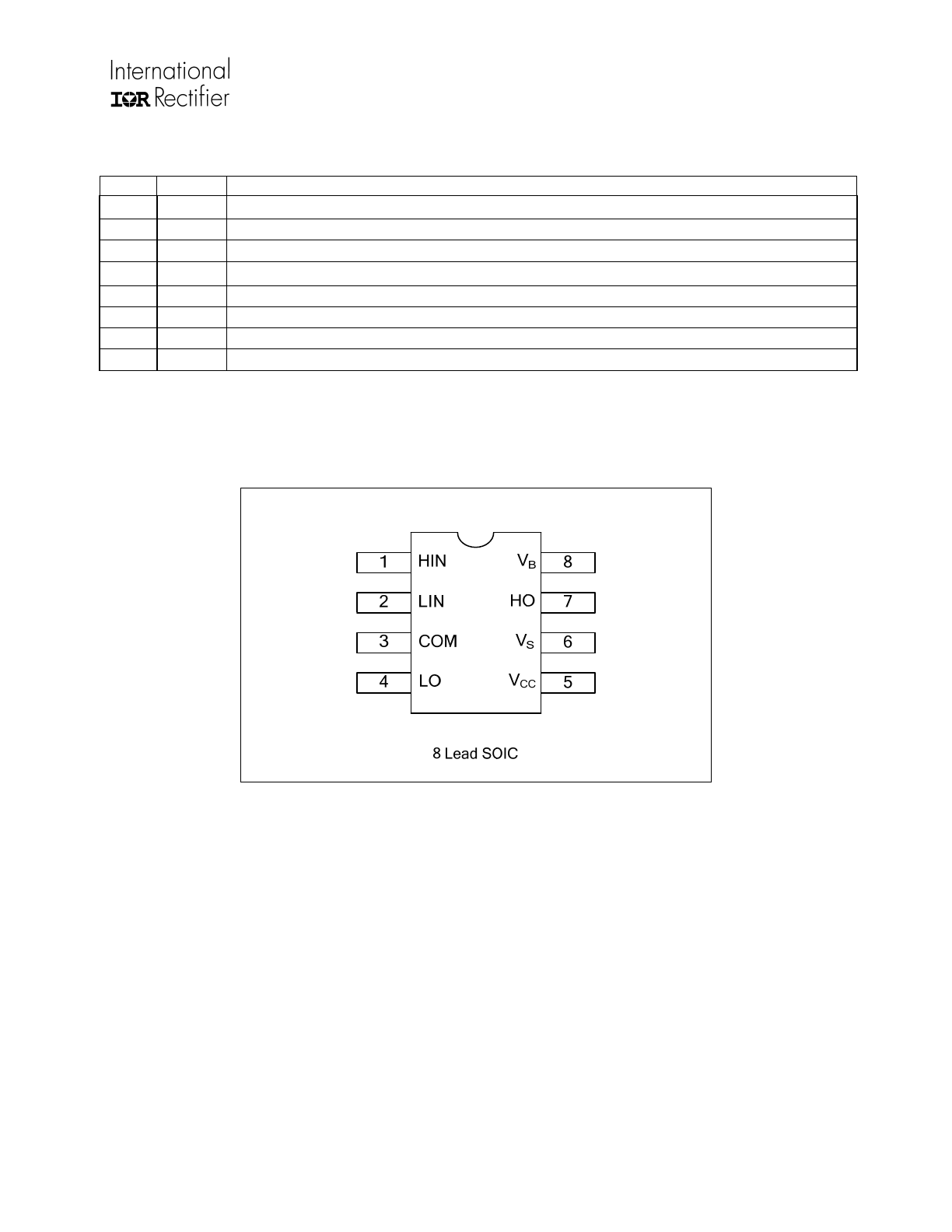
Lead Definitions: AUIRS21811S
Pin# Symbol
Description
1 HIN
Logic input for high-side driver output (HO), in phase
2 LIN
Logic input for low-side driver output (LO), in phase
3
COM Low-side
return
4
LO
Low-side gate drive output
5
V
CC
Low-side and logic fixed supply
6
V
S
High-side floating supply return
7
HO
High-side gate drive output
8
V
B
High-side floating supply
Lead Assignments
AUIRS21811S
www.irf.com
© 2009 International Rectifier
10
Application Information and Additional Details
Figure 1. Input/Output Timing Diagram
Figure 2. Switching Time Waveform Definitions
Figure 3. Delay Matching Waveform Definitions