
1
IR3837MPbF
Rev 1.31
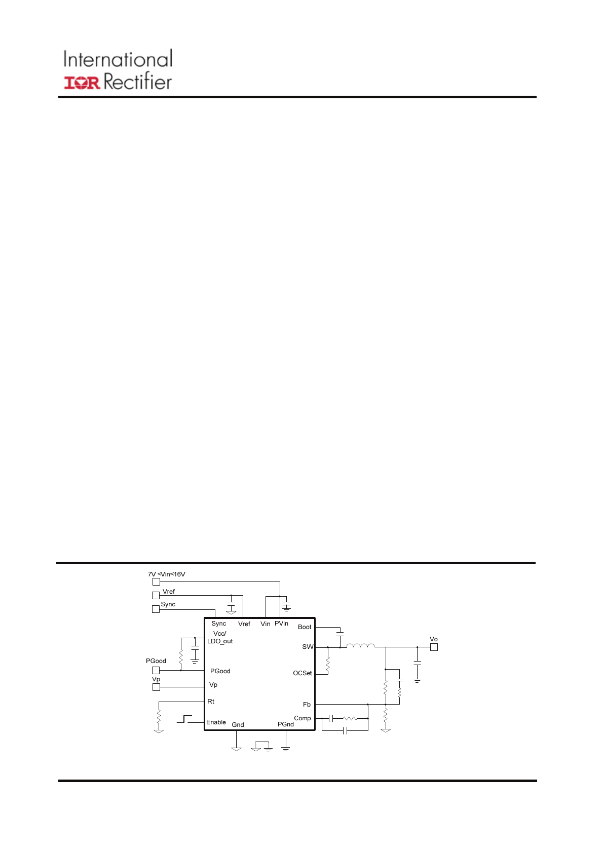
Fig. 1. Typical application diagram
Description
The IR3837 SupIRBuck
TM
is an easy-to-use, fully
integrated and highly efficient DC/DC regulator.
The onboard PWM controller and MOSFETs
make IR3837 a space-efficient solution, providing
accurate power delivery for low output voltage
applications.
IR3837 is a versatile regulator which offers
programmability of switching frequency and
current limit while operates in wide input and
output voltage range.
The switching frequency is programmable from
250kHz to 1.5MHz for an optimum solution.
It also features important protection functions,
such as Pre-Bias startup, hiccup current limit and
thermal shutdown to give required system level
security in the event of fault conditions.
IR3837 offers margining capability through Vref
pin. During the margining operation, PGood
tracks Vref via feedback to ensure correct status
of the output voltage.
The internal LDO enables the device to operate
from a single supply. This internal LDO can be
bypassed when an external bias voltage is
available.
Features
•
Greater than 96% Maximum Efficiency
•
Single 16V Application
•
Single 5V Application
•
Wide Output Voltage Range: 0.6V to 0.9*Vin
•
Continuous 14A Load Capability
•
Programmable Switching Frequency up to 1.5MHz
•
Internal Digital Soft-Start
•
Enable Input with Voltage Monitoring Capability
•
Hiccup Mode Over Current Protection
•
Internal LDO
•
External Synchronization
•
Enhanced PreBias Start up
•
External Reference for Margining Purposes
•
Input for Tracking Applications
•
Integrated MOSFET Drivers and Bootstrap Diode
•
Operating Junction Temp: -40
o
C <Tj<125
o
C
•
Thermal Shut Down
•
Power Good Output with Tracking Capability
•
Over Voltage Detection Feature
•
Pin Compatible with 6A and 10A Versions
•
Small Size 5mmx6mm PQFN, 0.9 mm Height
•
Lead-free, Halogen-free and RoHS Compliant
Applications
•
Netcom and Telecom Applications
•
Data Center Applications
•
Distributed Point of Load Power Architectures
HIGHLY INTEGRATED 14A
SINGLE-INPUT VOLTAGE, SYNCHRONOUS BUCK REGULATOR
SupIRBuck
TM
PD97511
2
IR3837MPbF
Rev 1.31
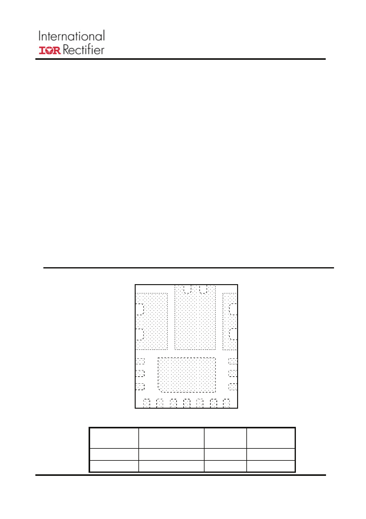
Package Information
5mm x 6mm Power QFN
(Top View)
13
PVin
12
SW
11
PGnd
17
Gnd
1
2
3
4
5
6
7
8
9
16
15
Fb Vref Comp Gnd Rt OCset PGood
Sync
Vin
Vp
Boot
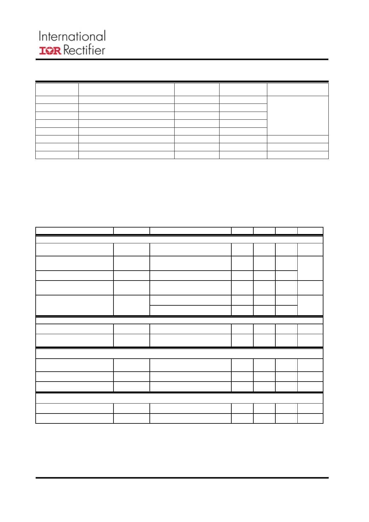
ABSOLUTE MAXIMUM RATINGS
(Voltages referenced to GND unless otherwise specified)
•
PVin, Vin ……………………………………………… -0.3V to 25V
•
Vcc/LDO_out ……………….……..……..……….…… -0.3V to 8V (Note2)
•
Boot ……………………………………..……….….. -0.3V to 33V
•
SW …………………………………………..……… -0.3V to 25V (DC), -4V to 25V (AC, 100ns)
•
Boot to SW ……..…………………………… …..…. -0.3V to Vcc+0.3V (Note1)
•
OCset
…………………………………………..…… -0.3V to 30V
•
Input / output Pins ………………………………... ... -0.3V to Vcc+0.3V (Note1)
•
PGnd to Gnd ……………...………………….…….…. -0.3V to +0.3V
•
Storage Temperature Range .................................... -55°C To 150°C
•
Junction Temperature Range ................................... -40°C To 150°C (Note2)
•
ESD Classification …………………………… ……… JEDEC(2KV)
•
Moisture sensitivity level………………...……………. JEDEC Level 2 @260 °C (Note 5)
Stresses beyond those listed under “Absolute Maximum Ratings” may cause permanent damage to the
device. These are stress ratings only and functional operation of the device at these or any other conditions
beyond those indicated in the operational sections of the specifications are not implied.
Note1:
Must not exceed 8V
Note2:
Vcc must not exceed 7.5V for Junction Temperature between -10
o
C and -40
o
C
Enable
Vcc/LDO_out
10
14
W
/
C
2
θ
W
/
C
35
θ
o
PCB
J
o
JA
=
=
-
4000
17
IR3837MTRPbF
M
750
PARTS PER
REEL
17
PIN
COUNT
IR3837MTR1PbF
PACKAGE
DESCRIPTION
M
PACKAGE
DESIGNATOR
ORDERING INFORMATION
3
IR3837MPbF
Rev 1.31
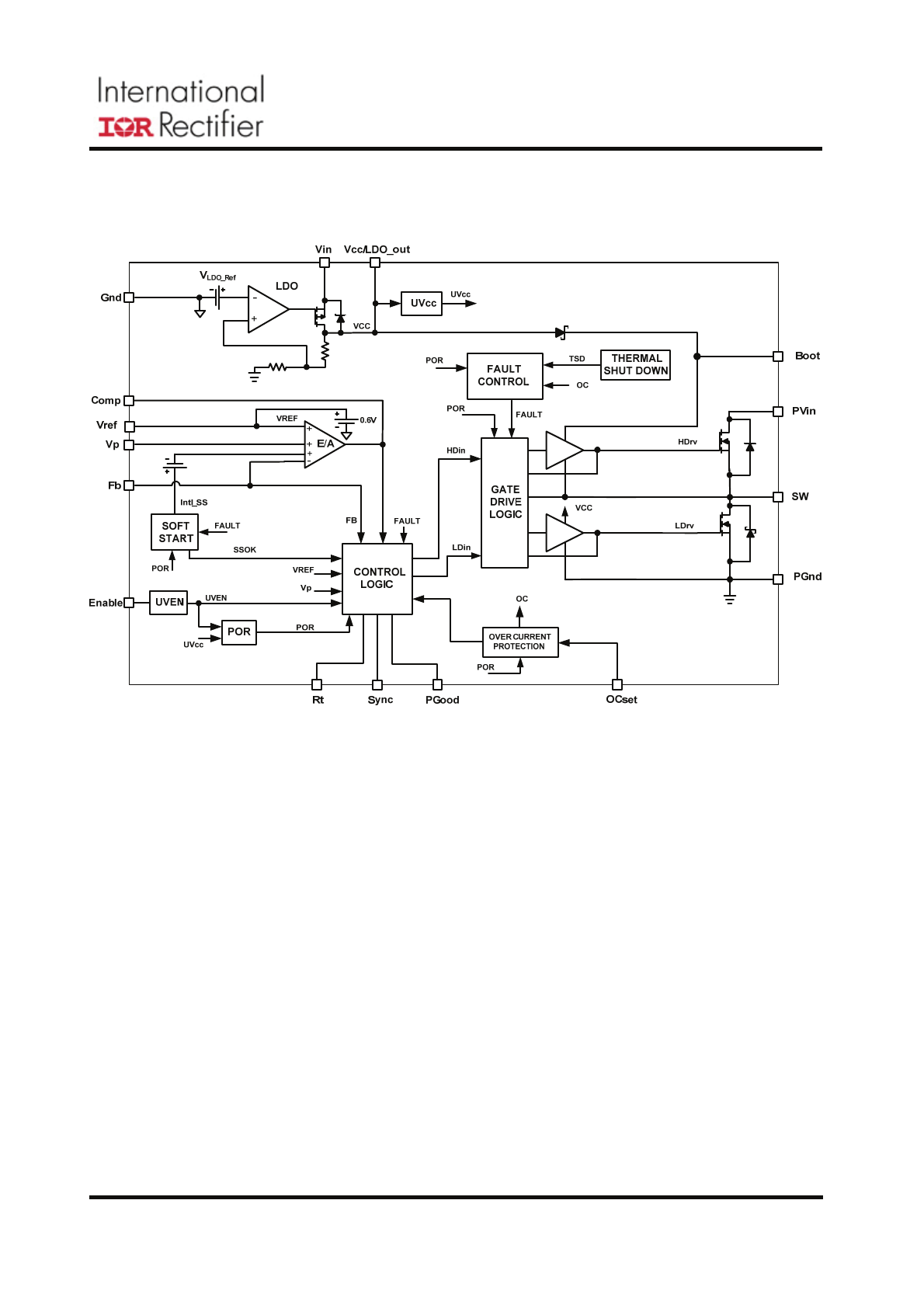
Block Diagram
Fig. 2. Simplified block diagram of the IR3837
4
IR3837MPbF
Rev 1.31
Pin Description
Pin Name
Description
1 Fb
Inverting input to the error amplifier. This pin is connected directly to the
output of the regulator via resistor divider to set the output voltage and
provide feedback to the error amplifier
2 Vref
External reference voltage, can be used for margining operation. A
100nF capacitor should be connected between this pin and Gnd.
3 Comp
Output of error amplifier. An external resistor and capacitor network is
typically connected from this pin to Fb to provide loop compensation
4
Gnd
Signal ground for internal reference and control circuitry
5
Rt
Use an external resistor from this pin to Gnd to set the switching
frequency
6
OCset
Current limit set point. A resistor from this pin to SW pin will set the
current limit threshold
7
PGood
Power Good status pin. Output is open drain. Connect a pull up resistor
from this pin to Vcc
8
Sync
External Synchronization, this pin is used to synchronize the device’s
switching with an external clock. It is recommended that the external
Sync clock be set to 20% above the free-running frequency. If not used,
this pin can be left floating.
9
Vin
Input voltage for Internal LDO. A 1.0µF capacitor should be connected
between this pin and PGnd. If external supply is connected to
Vcc/LDO_out pin, this pin should be left floating.
10
V
CC
/LDO_out
Input Bias Voltage, output of internal LDO. Place a minimum 2.2µF cap
from this pin to PGnd
11
PGnd
Power Ground. This pin serves as a separated ground for the MOSFET
drivers and should be connected to the system’s power ground plane.
12
SW
Switch node. This pin is connected to the output inductor
13
PVin
Input voltage for power stage
14 Boot
Supply voltage for high side driver, a 100nF capacitor should be
connected between this pin and SW pin.
15 Enable
Enable pin to turn on and off the device, if this pin is connected to PVin
pin through a resistor divider, input voltage UVLO can be implemented.
16
Vp
Input to error amplifier for tracking purposes
17
Gnd
Signal ground for internal reference and control circuitry
5
IR3837MPbF
Rev 1.31
Recommended Operating Conditions
Symbol Definition Min
Max Units
PVin
Input Voltage for power stage
1.5
16
Vin
Input Voltage for internal LDO *
7.0
16
Vcc/LDO_out Supply Voltage *
4.5
6.5
Boot to SW
Supply Voltage
4.5
7.5
V
o
Output
Voltage
0.6
0.9*Vin
V
I
o
Output
Current
0 14
A
Fs Switching
Frequency
225 1650 kHz
T
j
Junction
Temperature
-40 125
o
C
* Vcc/LDO_out can be connected to an external regulated supply (≈ 5V). If so, the Vin input should be
left unconnected.
PARAMETER SYMBOL
TEST
CONDITION
MIN
TYP
MAX
UNIT
POWER STAGE
Power Losses
P
loss
V
in
=12V, V
o
=1.8V, I
o
=14A,
Fs=600kHz, L=0.51uH, Note4
3 W
Top Switch
R
ds(on)_Top
V
Boot
-V
sw
=5.0V,
I
D
=14A,Tj=25C
12 16
Bottom Switch
R
ds(on)_Bot
V
cc
=5.0V, I
D
=14A
5.3 7
mΩ
Bootstrap Diode Forward
Voltage
I(Boot)=
30mA
180 260 470 mV
SW=0V, Enable=0V
6
SW leakage Current
Isw
SW=0V, Enable=high, Vp=0V
14
µA
SUPPLY CURRENT
V
in
Supply Current (Standby)
I
in(Standby)
Enable low , No Switching,
400
µA
V
in
Supply Current (Dyn)
I
in(Dyn)
Enable high, Fs=500kHz,
Vin=12V
17 mA
INTERNAL REGULATOR (LDO)
Output Voltage
IntVcc
Vin(min)=7.0V, Io=0-50mA,
Cload=2.2uF
4.7 5.2 5.7 V
IntVcc Dropout
IntVcc_drop
Io=50mA, Cload=2.2uF
50
150
mV
Short Circuit Current
Ishort
70
mA
INTERNAL DIGITAL SOFT START
Soft Start Clock Frequency
Clk(SS)
Note4
168
200
254
kHz
Soft Start Ramp Rate
Ramp(SS)
0.2
mV/us
Electrical Specifications
Unless otherwise specified, these specification apply over, 7.0V<V
in
=PVin<16V, Vref=0.6V
in 0
o
C<T
j
< 125
o
C. Typical values are specified at T
a
= 25
o
C.
6
IR3837MPbF
Rev 1.31
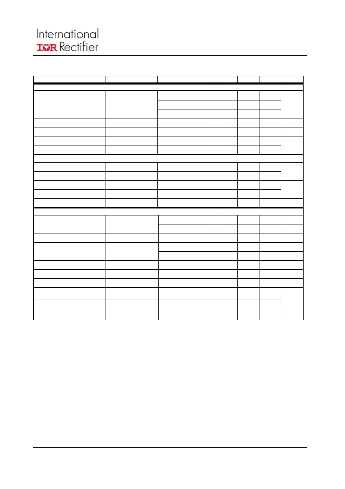
Electrical Specifications (continued)
Unless otherwise specified, these specification apply over, 7.0V<V
in
=PVin<16V, Vref=0.6V
in 0
o
C<T
j
< 125
o
C. Typical values are specified at T
a
= 25
o
C.
PARAMETER SYMBOL
TEST
CONDITION
MIN
TYP
MAX
UNIT
ERROR AMPLIFIER
Vos_Vp
Vfb-Vp, Vp=0.6V, Vref >2.0V
-1
+1
Input Offset Voltage
Vos_Vref Vfb-Vref,
Vref=0.6V,
Vp>2.0V -1 1
%
Input Bias Current
IFb(E/A)
-1
+1
A
Input Bias Current
IVp(E/A)
-1
+1
A
Sink Current
Isink(E/A)
0.40
0.85
1.2
mA
Source Current
Isource(E/A)
8
10
13
mA
Slew Rate
SR
Note4
7 12 20 V/
s
Gain-Bandwidth Product
GBWP
Note4
20 30 40 MHz
DC Gain
Gain
Note4
100 110 120 dB
Maximum Voltage
Vmax(E/A)
3.4 3.5 3.75 V
Minimum Voltage
Vmin(E/A)
150
220
mV
Common Mode Voltage
0
1.2
V
OSCILLATOR
Rt Voltage
0.665
0.7
0.735
V
Rt=59K
225 250 275
Rt=28.7K
450 500 550
Frequency Range
F
S
Rt=9.53K, Note4
1350
1500
1650
kHz
Ramp Amplitude
Vramp
Note4
1.8 Vp-p
Ramp Offset
Ramp(os)
Note4
0.6 V
Min Pulse Width
Dmin(ctrl)
Note4
70
ns
Max Duty Cycle
Dmax
Fs=250kHz
91
%
Fixed Off Time
Note4
300
ns
Sync Frequency Range
20% above free running
frequency
225 1650
kHz
Sync Pulse Duration
100
200
ns
Sync High
2
Sync Level Threshold
Sync Low
0.6
V
REFERENCE VOLTAGE
Feedback Voltage
VFB
Vref pin floating, Vp=Vcc
0.6
V
0
o
C<Tj<125
o
C -1.0
+1.0
Accuracy
-40
o
C<Tj<125
o
C, Note3
-2.0
+2.0
%
Vref margining voltage
Vref_marg
0.54
1.2
V
Sink Current
Isink_Vref
Vref=0.7V
19
25
µA
Source Current
Isource_Vref
Vref=0.5V
19
25
µA
Tracker(upper) Vref
pulled
up
externally
1.35 1.5 1.6
Tracker Comparator Threshold
Tracker(lower) Vref
pulled
up
externally
1.05 1.2 1.3
V
Tracker Comparator
Hysteresis
Tracker_Hys
Vref pulled up externally
220
300
420
mV
7
IR3837MPbF
Rev 1.31
Electrical Specifications (continued)
PARAMETER SYMBOL
TEST
CONDITION
MIN
TYP
MAX
UNIT
FAULT PROTECTION
Fs=250kHz
10.4 11.8 13.2
Fs=500kHz
21.5 24.4 27.3
OCSET Current
I
OCSET
Fs=1500kHz 68
77
86
µA
OC comp Offset Voltage
V
OFFSET
Note4
-6 0 +6 mV
SS off time
SS_Hiccup
4096
Cycles
Thermal Shutdown
Note4
140
Thermal Hysteresis
Note4
20
°C
UNDER VOLTAGE LOCKOUT
V
CC
-Start-Threshold V
CC
_UVLO_Start
Vcc Rising Trip Level
4.06
4.26
4.46
V
CC
-Stop-Threshold V
CC
_UVLO_Stop
Vcc Falling Trip Level
3.76
3.96
4.16
V
Enable-Start-Threshold Enable_UVLO_Start
Supply
ramping
up
1.14 1.2 1.36
Enable-Stop-Threshold
Enable_UVLO_Stop
Supply
ramping
down 0.75 0.85 0.95
V
Enable leakage current
Ien
Enable=3.3V
10
µA
PGOOD
Fb Rising, Vref < 1.2V
115
%Vref
Power Good upper Threshold
VPG(upper)
Fb Rising, Vref > 1.5V
115
%Vp
Upper Threshold Delay
VPG(upper)_Dly
Fb Falling
256/Fs
s
Fb Rising, Vref < 1.2V
85
%Vref
Power Good lower Threshold
VPG(lower)
Fb Rising, Vref > 1.5V
85
%Vp
Lower Threshold Delay
VPG(lower)_Dly
Fb Rising
256/Fs
s
Soft Start Delay Time
Tdelay(Delay)
Note4
10
ms
PGood Voltage Low
PG(voltage)
I
Pgood
=-5mA
0.5
V
Tracker Comparator Upper
Threshold
VPG(tracker_upper) Vp Rising, Vref > 1.5V
0.5
Tracker Comparator Lower
Threshold
VPG(tracker_lower) Vp Falling, Vref > 1.5V
0.3
V
Tracker Comparator Delay
Tdelay(tracker)
Vp Rising, Vref > 1.5V
256/Fs
s
Note3: Cold temperature performance is guaranteed via correlation using statistical quality control. Not tested in production.
Note4: Guaranteed by design but not tested in production
Note5: Upgrade to industrial/MSL2 level applies from date codes 1141 (marking explained on application note
AN1132
page 2).
Products with prior date code of 1141 are qualified with MSL3 for Consumer market.
8
IR3837MPbF
Rev 1.31
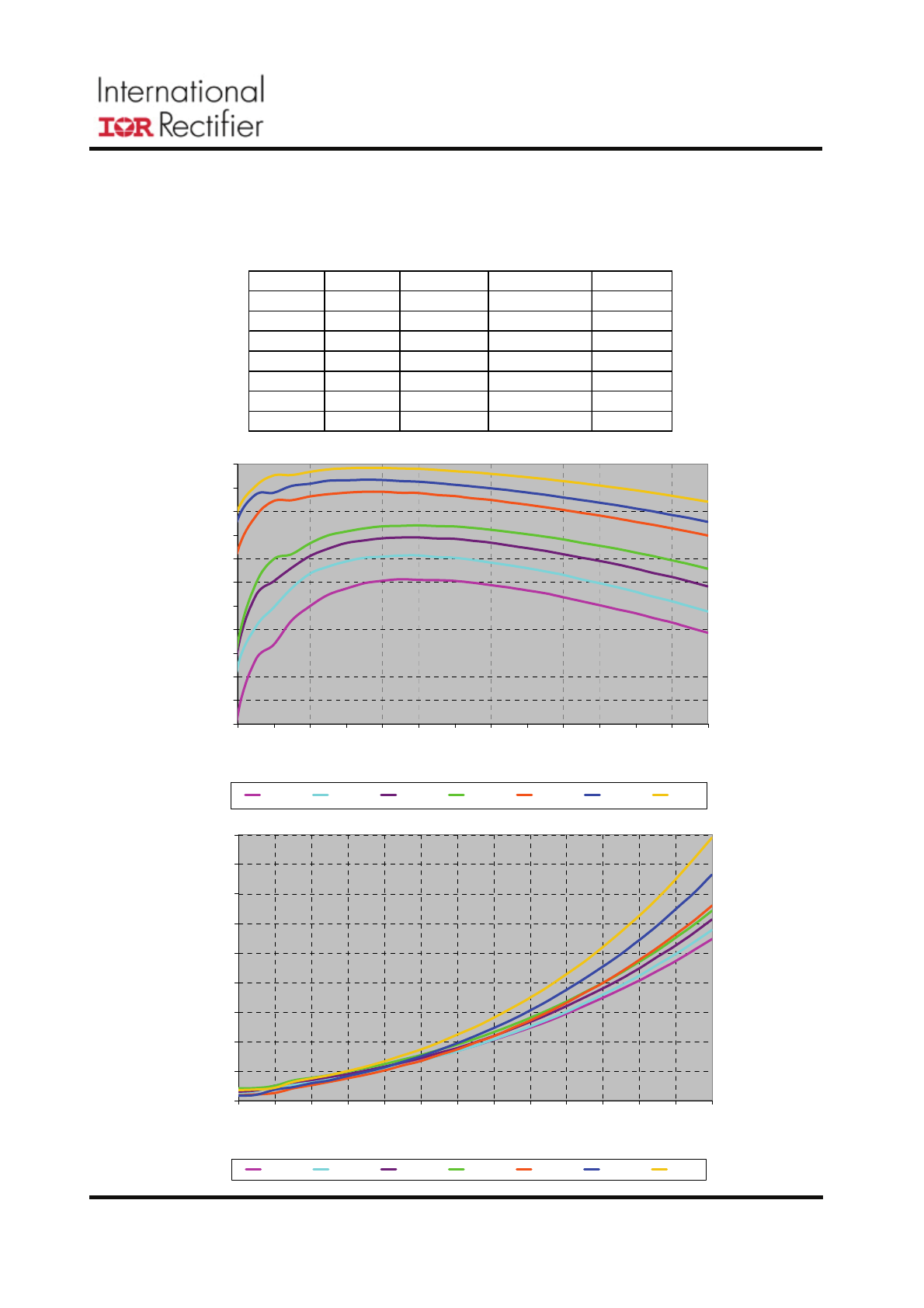
Typical Efficiency and Power Loss Curves
Vin=12V, Vcc=5V (external), Io=1A-14A, F
s
=600kHz, Room Temperature, No Air Flow
The table below shows the inductors used for each of the output voltages
in the efficiency measurement.
Vo [V]
L [µH]
MFR
P/N
DCR [mΩ]
1.0
0.4
Vitec
59PR9875N
0.29
1.2
0.51
Vitec
59PR9876N
0.29
1.5
0.51
Vitec
59PR9876N
0.29
1.8
0.51
Vitec
59PR9876N
0.29
2.5
0.68
Wurth Elek. 744 332 0068
0.72
3.3
1.0
Wurth Elek. 744 332 0100
1.17
5.0
1.0
Wurth Elek. 744 332 0100
1.17
75
77
79
81
83
85
87
89
91
93
95
97
1
2
3
4
5
6
7
8
9
10
11
12
13
14
Load Current (A)
Eff
iciency
(%
)
1.0V
1.2V
1.5V
1.8V
2.5V
3.3V
5.0V
0.2
0.7
1.2
1.7
2.2
2.7
3.2
3.7
4.2
4.7
1
2
3
4
5
6
7
8
9
10
11
12
13
14
Load Current (A)
Po
wer
Loss (
W
)
1.0V
1.2V
1.5V
1.8V
2.5V
3.3V
5.0V
9
IR3837MPbF
Rev 1.31
Typical Efficiency and Power Loss Curves
Vin=12V, Vcc/LDO_out=5.2V, Io=1A-14A, Fs=600kHz, Room Temperature, No Air Flow
The same inductors as listed on the previous page have been used.
71
73
75
77
79
81
83
85
87
89
91
93
95
97
1
2
3
4
5
6
7
8
9
10
11
12
13
14
Load Current (A)
Ef
fic
iency
(%
)
1.0V
1.2V
1.5V
1.8V
2.5V
3.3V
5.0V
0.2
0.7
1.2
1.7
2.2
2.7
3.2
3.7
4.2
4.7
1
2
3
4
5
6
7
8
9
10
11
12
13
14
Load Current (A)
Power
Loss
(W
)
1.0V
1.2V
1.5V
1.8V
2.5V
3.3V
5.0V
10
IR3837MPbF
Rev 1.31
Iin(Dyn)
15.8
16.0
16.2
16.4
16.6
16.8
17.0
-40
-20
0
20
40
60
80
100
120
140
Temp [ºC]
[m
A
]
TYPICAL OPERATING CHARACTERISTICS (-40
o
C - 125
o
C), F
s
=500 kHz
Iin(Standby)
160
180
200
220
240
260
280
300
320
340
360
380
400
-40
-20
0
20
40
60
80
100
120
140
Temp [ºC]
[µ
A
]
FREQUENCY
450
460
470
480
490
500
510
520
530
540
550
-40
-20
0
20
40
60
80
100
120
140
Temp [ºC]
[k
H
z]
IOCSET(500kHz)
21.5
22.5
23.5
24.5
25.5
26.5
27.5
-40
-20
0
20
40
60
80
100
120
140
Temp [ºC]
[µA
]
Vcc(UVLO) Start
4.06
4.11
4.16
4.21
4.26
4.31
4.36
4.41
4.46
-40
-20
0
20
40
60
80
100
120
140
Temp [ºC]
[V
]
Vcc(UVLO) Stop
3.76
3.81
3.86
3.91
3.96
4.01
4.06
4.11
4.16
-40
-20
0
20
40
60
80
100
120
140
Temp [ºC]
[V
]
Enable(UVLO) Start
1.14
1.16
1.18
1.20
1.22
1.24
1.26
1.28
1.30
1.32
1.34
1.36
-40
-20
0
20
40
60
80
100
120
140
Temp [ºC]
[V
]
Enable(UVLO) Stop
0.75
0.77
0.79
0.81
0.83
0.85
0.87
0.89
0.91
0.93
0.95
-40
-20
0
20
40
60
80
100
120
140
Temp [ºC]
[V
]
Vcc_LDO
4.7
4.8
4.9
5.0
5.1
5.2
5.3
5.4
5.5
5.6
5.7
-40
-20
0
20
40
60
80
100
120
140
Temp [ºC]
[V
]
Vfb
0.588
0.592
0.596
0.600
0.604
0.608
0.612
-40
-20
0
20
40
60
80
100
120
140
Temp [ºC]
[V
]