

Standard Power
Data Sheet
Rev 1.0, 2012-09-01
ITS41k0S-ME-N
Smart High-Side NMOS-Power Switch

PG-SOT223-4
Data Sheet
2
Rev 1.0, 2012-09-01
Smart High-Side NMOS-Power Switch
ITS41k0S-ME-N
Type
Package
Marking
ITS41k0S-ME-N
PG-SOT223-4
I1k0SN
1
Overview
Features
•
Current controlled input
•
Capable of driving all kind of loads (inductive, capacitive and resitive)
•
Negative voltage clamped at output with inductive loads
•
Current limitation
•
Very low standby current
•
Thermal shutdown with restart
•
Overload protection
•
Short circuit protection
•
Overvoltage protection (including load dump)
•
Reverse battery protection
•
Loss of GND and loss of Vbb protection
•
ESD-Protection
•
Improved electromagnetic compatibility (EMC)
•
Green Product (RoHS compliant)
ITS41k0S-ME-N is not qualified and manufactured according to the requirements of Infineon Technologies with
regards to automotive and/or transportation applications.
Description
The ITS41k0S-ME-N is a protected 1 Ω single channel Smart High-Side NMOS-Power Switch in a PG-SOT223-
4 package with charge pump and current controlled input, monolithically integrated in a smart power technology.
Product Summary
Overvoltage protection
V
SAZ
min
= 62V
Operating voltage range 4,9V <
V
S
< 60V
On-state resistance
R
DSON
typ 800 mΩ
Operating Temperature range Tj = -40°C to 125°C
Application
•
All types of resistive, inductive and capacitive loads
•
Current controlled power switch for 12V, 24V and 45V DC in industrial applications
•
Driver for electromagnetic relays
•
Signal amplifier
Data Sheet
3
Rev 1.0, 2012-09-01
ITS41k0S-ME-N
Block Diagram and Terms
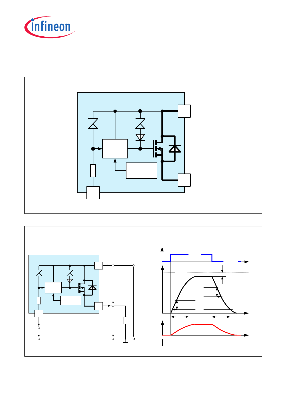
2
Block Diagram and Terms
Figure 1
Block diagram
Figure 2
Terms - parameter definition
3
ITS41k0S-ME-N
1
Control
Circuit
R
IN
2, 4
Temperature
Sensor
IN
OUT
V
S
I
IN
V
IN
V
OU
T
V
S
I
S
I
L
R
L
V
DS
GND
IN
OUT
V
S
Voltage- and Current-Definitions:
Switching Times and Slew Rate Definitions:
OFF
OFF
ON
V
DS
V
OUT
90%
0
+V
S
10%
t
OFF
I
IN
0
I
INOFF
I
INON
t
I
L
t
0
t
ON
SR
ON
30%
SR
OFF
70%
40%
t
3
ITS41k0S-ME-N
1
Control
Circuit
R
IN
2, 4
Temperature
Sensor
Data Sheet
4
Rev 1.0, 2012-09-01
ITS41k0S-ME-N
Pin Configuration
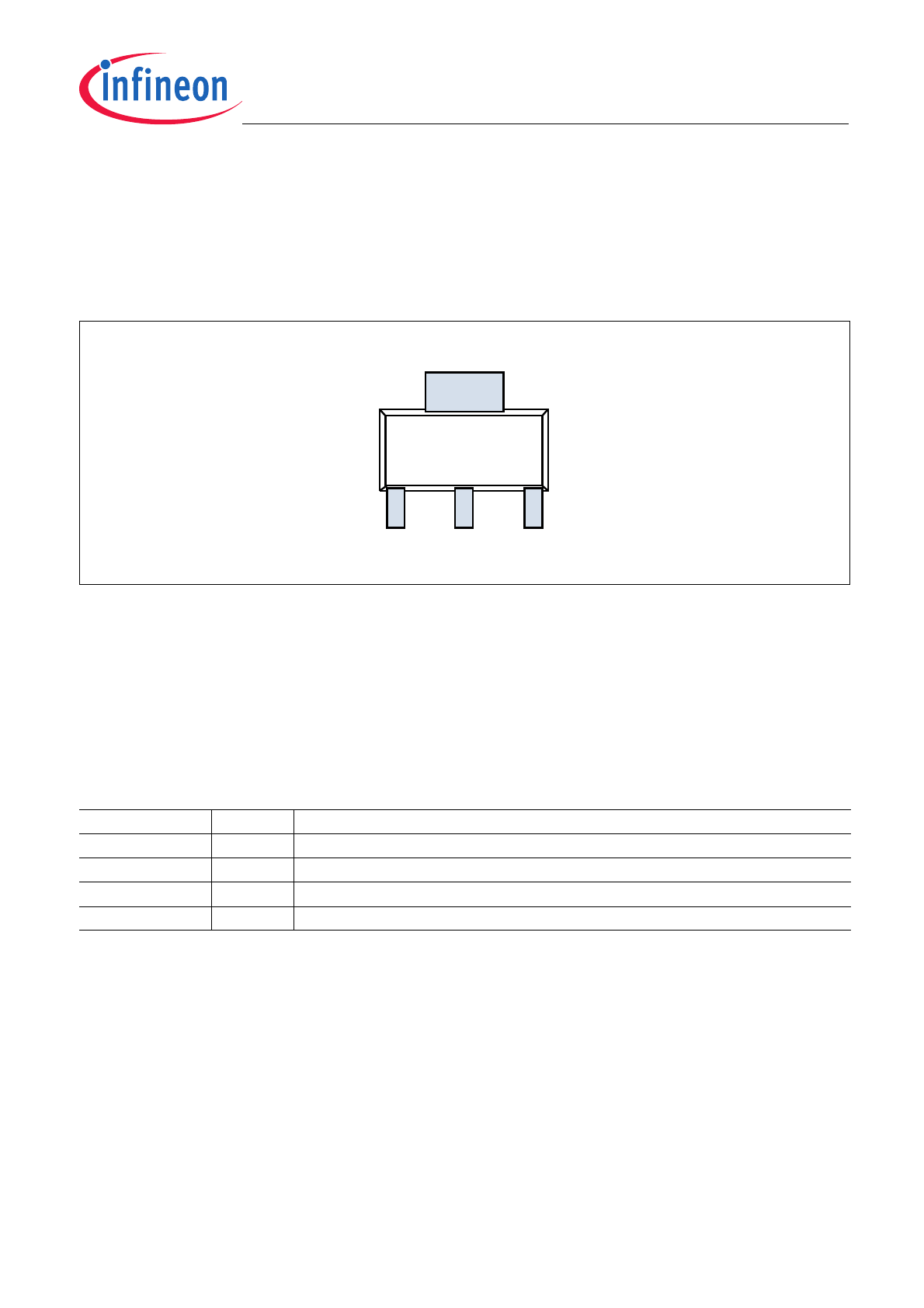
3
Pin Configuration
3.1
Pin Assignment
Figure 3
Pin configuration top view, PG-SOT223-4
3.2
Pin Definitions and Functions
Pin
Symbol
Function
1
IN
Input, activates the power switch in case of connection to GND
2
VS
Supply voltage
3
OUT
Output to the load
4
VS
Supply voltage
1
2
3
4

Data Sheet
5
Rev 1.0, 2012-09-01
ITS41k0S-ME-N
General Product Characteristics
4
General Product Characteristics
4.1
Absolute Maximum Ratings
Note: Exposure to absolute maximum rating conditions for extended periods may affect device reliability.
Integrated protection functions are designed to prevent IC destruction under fault conditions described in the
data sheet. Fault conditions are considered as “outside” the normal operating range. Protection functions
are not designed for continuous or repetitive operation.
Table 1
Absolute maximum ratings
1)
Tj = 25°C all voltages with respect to ground.
Currents flowing into the device unless otherwise specified in chapter “Block Diagram and
Terms”
1) Not subject to production test, specified by design
Parameter
Symbol
Values
Unit
Note /
Test Co
ndition
Min.
Typ.
Max.
Supply voltage VS
Voltage
V
S
60
V
4.1.1
Output stage OUT
Output Current; (Short circuit current see
electrical characteristics)
I
OUT
self limited
A
4.1.2
Input IN
Input Current
I
IN
-15
15
mA
4.1.3
Temperatures
Junction Temperature
T
j
-40
125
°C
4.1.4
Storage Temperature
T
stg
-55
125
°C
4.1.5
Power dissipation
Ta = 25 °C
2)
2)
Device on 50mm*50mm*1.5mm epoxy PCB FR4 with 6 cm2 (one layer, 70mm thick) copper area for Vbb
connection. PCB is vertical without blown air
P
tot
1.7
W
4.1.6
Inductive load switch-off energy dissipation
Tj = 150 °C; IL=0.15A; single pulse
1)
E
AS
1000
mJ
4.1.7
ESD Susceptibility
ESD susceptibility (input pin)
V
ESD
-1
1
kV
HBM
3)
3) ESD susceptibility HBM according to EIA/JESD 22-A 114.
4.1.8
ESD susceptibility (all other pins)
V
ESD
-5
5
kV
HBM
3)
4.1.9
Data Sheet
6
Rev 1.0, 2012-09-01
ITS41k0S-ME-N
General Product Characteristics
4.2
Functional Range
Note: Within the functional range the IC operates as described in the circuit description. The electrical
characteristics are specified within the conditions given in the related electrical characteristics table.
4.3
Thermal Resistance
This thermal data was generated in accordance with JEDEC JESD51 standards.
More information on www.jedec.org.
Table 2
Functional Range
Parameter
Symbol
Values
Unit
Note /
Test Condition
Number
Min.
Typ.
Max.
Nominal Operating Voltage
V
S
4.9
–
60
V
V
S
increasing
4.2.1
Table 3
Thermal Resistance
1)
1) Not subject to production test, specified by design
Parameter
Symbol
Values
Unit
Note /
Test Condition
Number
Min.
Typ.
Max.
PG-SOT223-4
Junction to Case, Exposed pad
R
thjc
–
40.5
–
K/W
4.3.1
Junction to ambient
R
thJA_1s0p
–
145.4 –
K/W
2)
2) Specified
R
thJA
value is according to Jedec JESD51-3 at natural convection on FR4 1s0p board, footprint; the Product
(Chip+Package) was simulated on a 76.2 x 114.3 x 1.5 mm board with 1x 70µm Cu.
4.3.2
Junction to ambient
R
thJA_1s0p_300mm
–
77.2
–
K/W
3)
3) Specified
R
thJA
value is according to Jedec JESD51-3 at natural convection on FR4 1s0p board, Cu, 300mm
2
; the Product
(Chip+Package) was simulated on a 76.2 x 114.3 x 1.5 mm board with 1x 70µm Cu.
4.3.3
Junction to ambient
R
thJA_1s0p_600mm
–
66.2
–
K/W
4)
4) Specified
R
thJA
value is according to Jedec JESD51-3 at natural convection on FR4 1s0p board, 600mm
2
; the Product
(Chip+Package) was simulated on a 76.2 x 114.3 x 1.5 mm board with 1x 70µm Cu.
4.3.4
Junction to ambient
R
thJA_2s2p
–
57.8
–
K/W
5)
5) Specified
R
thJA
value is according to Jedec JESD51-2,-5,-7 at natural convection on FR4 2s2p board; the Product
(Chip+Package) was simulated on a 76.2 x 114.3 x 1.5 mm board with 2 inner copper layers (2 x 70µm Cu, 2 x 35µm Cu).
4.3.5
Junction to ambient
R
thJA_2s2pvia
–
52.9
–
K/W
6)
6) Specified
R
thJA
value is according to Jedec JESD51-2,-5,-7 at natural convection on FR4 2s2p board with two thermal
vias; the Product (Chip+Package) was simulated on a 76.2 x 114.3 x 1.5 mm board with 2 inner copper layers (2 x 70µm
Cu, 2 x 35µm Cu. The diameter of the two vias are equal 0.3mm and have a plating of 25um with a copper heatsink area
of 3mm x 2mm). JEDEC51-7: The two plated-through hole vias should have a solder land of no less than 1.25 mm
diameter with a drill hole of no less than 0.85 mm diameter.
4.3.6

Data Sheet
7
Rev 1.0, 2012-09-01
ITS41k0S-ME-N
Electrical Characteristics
5
Electrical Characteristics
Table 4
V
S
= 9V to 60V; Tj = -40°C to 125°C; all voltages with respect to ground. Currents flowing into
the device unless otherwise specified in chapter “Block Diagram and Terms”. Typical values
at Vs = 13.5V, Tj = 25°C
Parameter
Symbol
Values
Unit
Note /
Test Condition
Number
Min.
Typ.
Max.
Powerstage
NMOS ON Resistance
R
DSON
–
0.8
1.5
Ω
I
OUT
= 150mA;
T
j
= 25°C;
IN conected to GND
5.0.1
NMOS ON Resistance
R
DSON
–
1.5
3.0
Ω
I
OUT
= 150mA;
T
j
= 125°C;
IN conected to GND
5.0.2
NMOS ON Resistance
R
DSON
–
2
5
Ω
I
OUT
= 50mA;
T
j
= 25°C;
V
S
= 6V;
IN conected to GND
5.0.3
Nominal Load Current
1)
;
device on PCB
2)
I
LNOM
0.2
–
–
A
T
a
= 85°C;
T
j
= 125°C;
5.0.4
Timings of Power Stages
Turn ON Time
3)
(to 90% of
V
out
);
V
S
to GND transition of
V
IN
t
ON
–
–
125
4)
µs
V
S
=13.5V;
R
L
= 270Ω
5.0.5
Turn ON Time
3)
(to 90% of
V
out
);
V
S
to GND transition of
V
IN
t
ON
–
45
100
µs
V
S
=13.5V;
R
L
= 270Ω;
T
j
= 25°C
5.0.6
Turn OFF Time
3)
(to 10% of
V
out
);
GND to
V
S
transition of
V
IN
t
OFF
–
–
175
4)
µs
V
S
=13.5V;
R
L
= 270Ω
5.0.7
Turn OFF Time
3)
(to 10% of
V
out
);
GND to
V
S
transition of
V
IN
t
OFF
–
40
140
µs
V
S
=13.5V;
R
L
= 270Ω;
T
j
= 25°C
5.0.8
ON-Slew Rate
3)
(10 to 30% of
V
out
);
V
S
to GND transition of
V
IN
SR
ON
–
–
6
4)
V / µs
V
S
=13.5V;
R
L
= 270Ω
5.0.9
ON-Slew Rate
3)
(10 to 30% of
V
out
);
V
S
to GND transition of
V
IN
SR
ON
–
1.3
4.0
V / µs
V
S
=13.5V;
R
L
= 270Ω;
T
j
= 25°C
5.0.10
OFF-Slew Rate
3)
(70 to 40% of
V
out
);
GND to
V
S
transition of
V
IN
SR
OFF
–
–
8
4)
V / µs
V
S
=13.5V;
R
L
= 270Ω
5.0.11
OFF-Slew Rate
3)
(70 to 40% of
V
out
);
GND to
V
S
transition of
V
IN
SR
OFF
–
1.7
4.0
V / µs
V
S
=13.5V;
R
L
= 270Ω;
T
j
= 25°C
5.0.12
Standby current consumption

Data Sheet
8
Rev 1.0, 2012-09-01
ITS41k0S-ME-N
Electrical Characteristics
Standby current
I
SOFF
–
2
10
µA
IN open
5.0.13
Protection functions
5)
Initial peak short circuit current limit
IN conected to GND
I
LSCP
–
–
1.2
A
T
j
= -40°C
;
V
S
= 13.5V
t
m
= 100µs
5.0.14
Initial peak short circuit current limit
IN conected to GND
I
LSCP
–
0.9
–
A
T
j
= 25°C
;
V
S
= 13.5V
t
m
= 100µs
5.0.15
Initial peak short circuit current limit
IN conected to GND
I
LSCP
0.2
–
–
A
T
j
=125°C
;
V
S
= 13.5V
t
m
= 100µs
5.0.16
Repetitive short circuit current limit
IN conected to GND
I
LSCR
–
0.7
–
A
–
5.0.17
Output clamp at
V
OUT
=
V
S
-
V
DSCL
(inductive load switch off)
V
DSCL
60
–
–
V
I
S
= 4mA
5.0.18
Overvoltage protection
V
SAZ
62
68
–
V
I
S
= 1mA
5.0.19
Thermal overload
trip temperature
4)
T
jTrip
150
–
–
°C
–
5.0.20
Thermal hysteresis
4)
T
HYS
10
–
°C
–
5.0.21
Input interface
Off state input current
I
INOFF
–
–
0.05
mA
T
j
= -25°C
;
R
L
= 270Ω;
V
OUT
=< 0.1V
5.0.22
Off state input current
I
INOFF
–
–
0.04
mA
T
j
= 125°C
;
R
L
= 270Ω;
V
OUT
=< 0.1V
5.0.23
On state input current;
IN connected to GND
6)
I
INON
–
0.3
1.0
mA
–
5.0.24
Input resistance
R
IN
0.5
1.0
2.5
kΩ
–
5.0.25
Reverse Battery
Continuous reverse drain current
I
DREV
–
–
0.2
A
–
5.0.26
Forward voltage of the drain-source
reverse diode
V
FDS
–
600
–
mV
I
FDS
= 200mA
I
IN
=< 0.05mA
5.0.27
1) Nominal Load Current is limited by the current limitation; see protection function data
2) Device on 50mm x 50mm x 1,5mm epoxy FR4 PCB with 6cm² (one layer copper 70um thick) copper area for supply voltage
connection. PCB in vertical position without blown air
3) Timing values only with high input slewrates (
t
rIN
=
t
fIN
<= 50ns); otherwise slower
4) Not tested in production
5) Integrated protection functions are designed to prevent IC destruction under fault conditions described in the data sheet.
Fault conditions are considered as “outside” normal operating range. Protection functions are not designed for continuous
repetitive operation.
6) Driver circuit must be able to sink currents > 1mA
Table 4
V
S
= 9V to 60V; Tj = -40°C to 125°C; all voltages with respect to ground. Currents flowing into
the device unless otherwise specified in chapter “Block Diagram and Terms”. Typical values
at Vs = 13.5V, Tj = 25°C
Parameter
Symbol
Values
Unit
Note /
Test Condition
Number
Min.
Typ.
Max.
Data Sheet
9
Rev 1.0, 2012-09-01
ITS41k0S-ME-N
Application Information
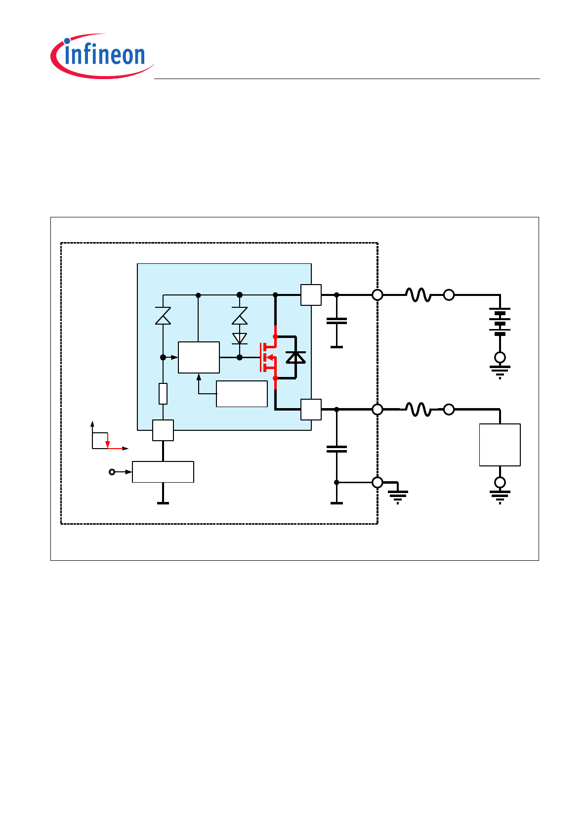
6
Application Information
6.1
Application Diagram
The following information is given as a hint for the implementation of the device only and shall not be regarded as
a description or warranty for a certain functionality, condition or quality of the device.
Figure 4
Application Diagram
The ITS41k0S-ME-N can be connected directly to a supply network. It is recommended to place a ceramic
capacitor (e.g.
C
S
= 220nF) between supply and GND to avoid line disturbances. Wire harness inductors/resistors
are sketched in the application circuit above.
The complex load (resistive, capacitive or inductive) must be connected to the output pin OUT.
A built-in current limit protects the device against destruction.
The ITS41k0S-ME-N can be switched on and off with a low power levelshifter switch e.g. Infineon BCR1xx.
The IN pin must be pulled down to GND potential to switch the ITS41k0S-ME-N on. If no current is pulled down,
the IN-node will float up to
V
S
potential by an internal pull up. In this mode the ITS41k0S-ME-N is deactivated with
very low current consumption.
The output voltage slope is controlled during on and off transistion to minimize emissions. Only a small Cercap
C
OUT
=1nF is recommended to attenuate RF noise.
In the following chapters the main features, some typical waverforms and the protection behaviour of the
ITS41k0S-ME-N is shown. For further details please refer to application notes on the Infineon homepage.
complexLOAD
3
ITS41k0S-ME-N
1
Control
Circuit
R
IN
Temperature
Sensor
IN
OUT
V
S
2, 4
Infineon
BCR 1xx
Vctrl
Wire
Harness
complex
LOAD
t
ON
OFF
Electronic Control Unit
Wire
Harness
GND 2
GND 3
C
S
220nF
C
OUT
1nF
GND 1
Vc
tr
l
Data Sheet
10
Rev 1.0, 2012-09-01
ITS41k0S-ME-N
Application Information
6.2
Special features
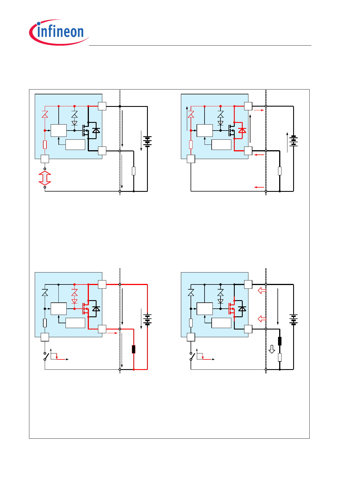
Figure 5
Special Feature descriptions
Energy stored in the load inductance is given by :
E
L
= I
L
²*L/2
While demagnetizing the load inductance the energy
dissipated by the Power -DMOS is:
E
AS
= E
S
+ E
L
– E
R
With an approximate solution for R
L
> 0
Ω:
E
AS
= (I
L
*L) / (2*R
L
)*(V
S
+V
DSCL
)*ln((1+(I
L
*R
L
) / V
DSCL
)
When an inductive load is switched off a current path
must be established until the current is sloped down
to zero (all energy removed from the inductive load ).
For that purpose the series combination ZD2 and D1
is connceted between Gate and Drain of the power
DMOS.
When the device is switched off, the voltage at OUT
turns negative until V
DSCL
is reached.
The Voltage on the incutive load is the difference
between V
DSCL
and V
S
.
If reverse Voltage is applied to the device :
1.) Current via Load Resistance RL :
I
Rev1
= (V
REV
– V
FM1
) / R
L
2.) Current via Input Resistance RIN :
I
REV2
= (V
REV
– V
FZD1
) / R
IN
Both currents will sum up to:
I
REV
= I
REV1
+ I
REV2
If Over-Voltage is applied to the V
S
-Pin:
Voltage is limited to VZD1; Current can be calculated :
I
ZD1
= (V
S
– V
ZD1
) / R
IN
In case of ESD Pulse on the input pin there is in both
polarities a peak current I
INpeak
~ V
ESD
/ R
IN
The control unit is protected in both cases by the
Zenerdiode ZD1
3
ITS41k0S-ME-N
1
Control
circuit
R
IN
2, 4
Temperature
Sensor
IN
OUT
V
S
3
ITS41k0S-ME-N
1
Control
circuit
R
IN
Temperature
Sensor
IN
OUT
V
S
Z
L
2, 4
I
REV1
I
REV2
V
RE
V
3
ITS41k0S-ME-N
1
Control
circuit
R
IN
Temperature
Sensor
IN
OUT
V
S
L
L
2, 4
I
L
V
Ba
tt
V
DS
C
L
V
OU
T
3
ITS41k0S-ME-N
1
Control
circuit
R
IN
Temperature
Sensor
IN
OUT
V
S
L
L
2, 4
E
R
R
L
t
ON
OFF
E
L
E
Batt
E
Load
Z
L
V
Ba
tt
V
DS
V
OU
T
V
ES
D
t
ON
OFF
ZD
1
ZD
2
D
1
M
1
ZD
1
ZD
2
D
1
M
1
ZD
1
ZD
2
D
1
M
1
ZD
1
ZD
2
D
1
M
1
V
DS
C
L
I
REV
V
FM
1
V
FZ
D
1