
Rev.1.0
Data Sheet No. PD60347A
IRS26310DJPbF
HIGH VOLTAGE 3 PHASE GATE DRIVER IC WITH DC BUS
OVER –VOLTAGE PROTECTION
Features
•
Drives up to six IGBT/MOSFET power devices
•
Gate drive supplies up to 20 V per channel
•
Integrated bootstrap functionality
•
DC bus sensing with Over Voltage protection
•
Over-current protection
•
Over-temperature shutdown input
•
Advanced input filter
•
Integrated deadtime protection
•
Shoot-through (cross-conduction) protection
•
Under voltage lockout for V
CC
& V
BS
•
Enable/disable input and fault reporting
•
Adjustable fault clear timing
•
Separate logic and power grounds
•
3.3 V input logic compatible
•
Tolerant to negative transient voltage
•
Designed for use with bootstrap power supplies
•
Matched propagation delays for all channels
•
-40 °C to 125 °C operating range
•
RoHS compliant
Typical Applications
•
Permanent magnet motor drives for appliances
•
Industrial drives
•
Micro inverter drives
Product Summary
Topology
3 Phase
V
OFFSET
≤ 600 V
V
OUT
12 V – 20 V
I
o+
& I
o-
(typical)
200 mA & 350 mA
t
ON
& t
OFF
(typical)
530 ns & 530 ns
Deadtime (typical)
290 ns
Package Options
44-Lead PLCC (without 12 leads)
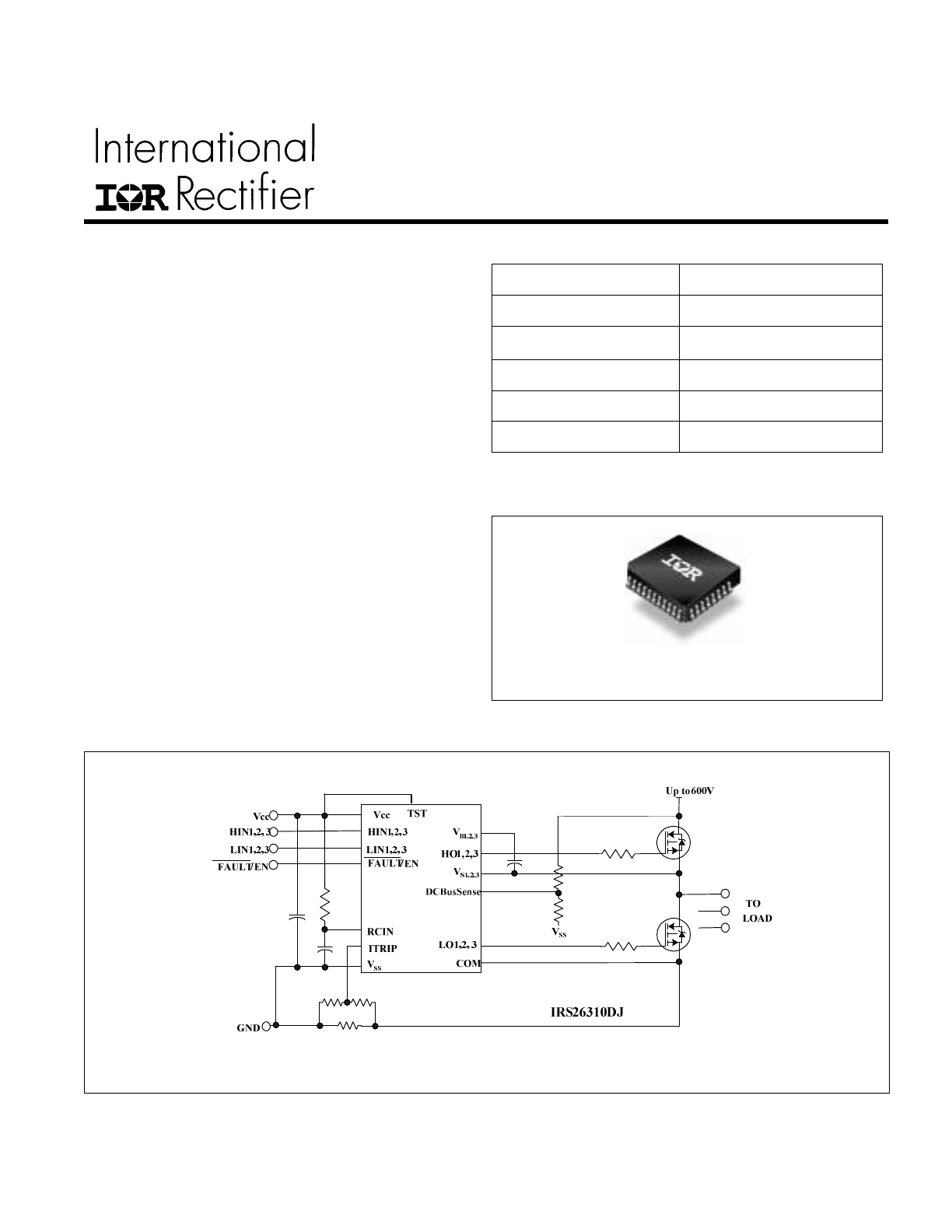
Typical Connection Diagram
Not recommended for new designs. For new designs, we recommend 6EDL04I06NT/PT

IRS26310DJPbF
www.irf.com
© 2007 International Rectifier
2
Table of Contents
Page
Description
3
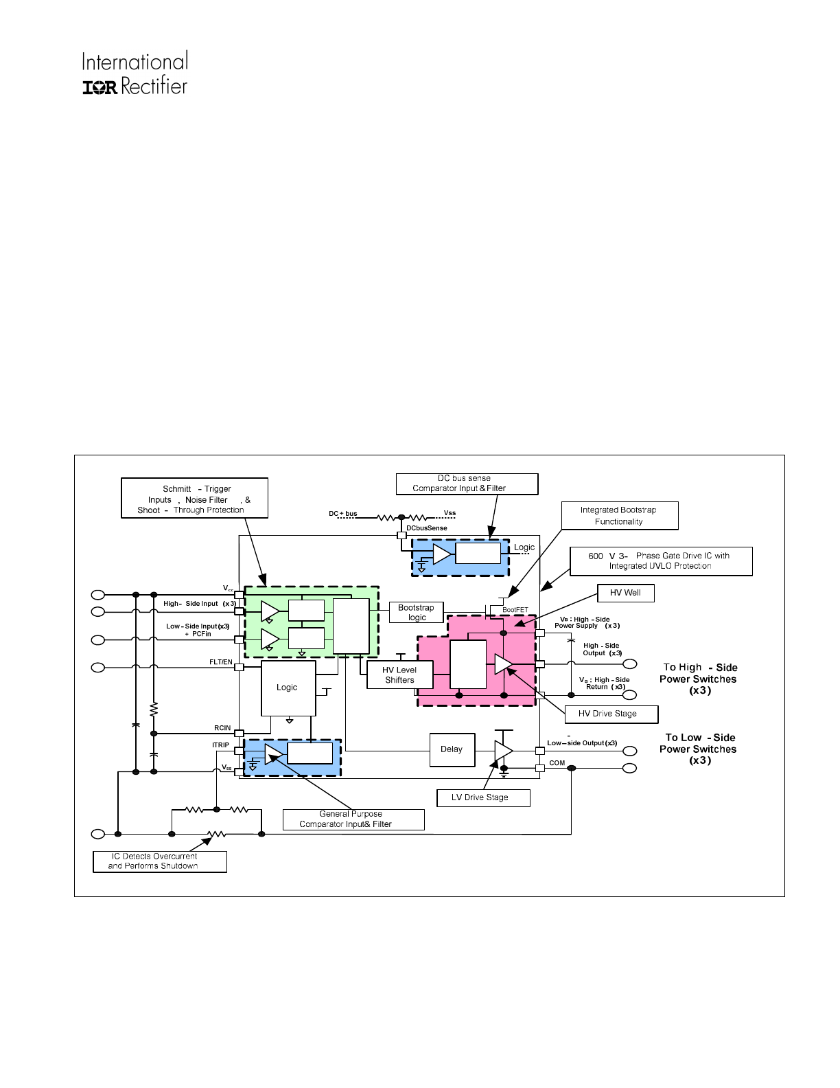
Simplified Block Diagram
3
Typical Application Diagram
4
Qualification Information
5
Absolute Maximum Ratings
6
Recommended Operating Conditions
7
Static Electrical Characteristics
8
Dynamic Electrical Characteristics
10
Functional Block Diagram
11
Input/Output Pin Equivalent Circuit Diagram
12
Lead Definitions
13
Lead Assignments
14
Application Information and Additional Details
15
Parameter Temperature Trends
36
Package Details
40
Tape and Reel Details
41
Part Marking Information
42
Ordering Information
43
Not recommended for new designs. For new designs, we recommend 6EDL04I06NT/PT
IRS26310DJPbF
www.irf.com
© 2007 International Rectifier
3
Description
The IRS26310DJPBF is a high voltage, high speed power MOSFET and IGBT driver with three independent
high and low side referenced output channels for 3-phase applications. This IC is designed to be used with
low-cost bootstrap power supplies; the bootstrap diode functionality has been integrated into this device to
reduce the component count and the PCB size. Proprietary HVIC technology enables ruggedized monolithic
construction. Logic inputs are compatible with CMOS or LSTTL outputs, down to 3.3V logic. A current trip
function which terminates all six outputs can be derived from an external current sense resistor. An enable
function is available to terminate all six outputs simultaneously. An open-drain FAULT signal is provided to
indicate that an overcurrent or a VCC undervoltage shutdown has occurred. Overcurrent fault conditions are
cleared automatically after a delay programmed externally via an RC network connected to the RCIN input.
The output drivers feature a high pulse current buffer stage designed for minimum driver cross-conduction.
Propagation delays are matched to simplify use in high frequency applications. The floating channel can be
used to drive N-channel power MOSFETs or IGBTs in the high side configuration which operates up to 600 V.
A DCbus sensing is provided using an external divider. Over Voltage DCbus protection is activate when
DCbus exceed an externally adjustable threshold, activating zero-vector braking mode (all Low side output
turn-on, all High side output-turn-off).
Simplified Block Diagram
Not recommended for new designs. For new designs, we recommend 6EDL04I06NT/PT
IRS26310DJPbF
www.irf.com
© 2007 International Rectifier
4
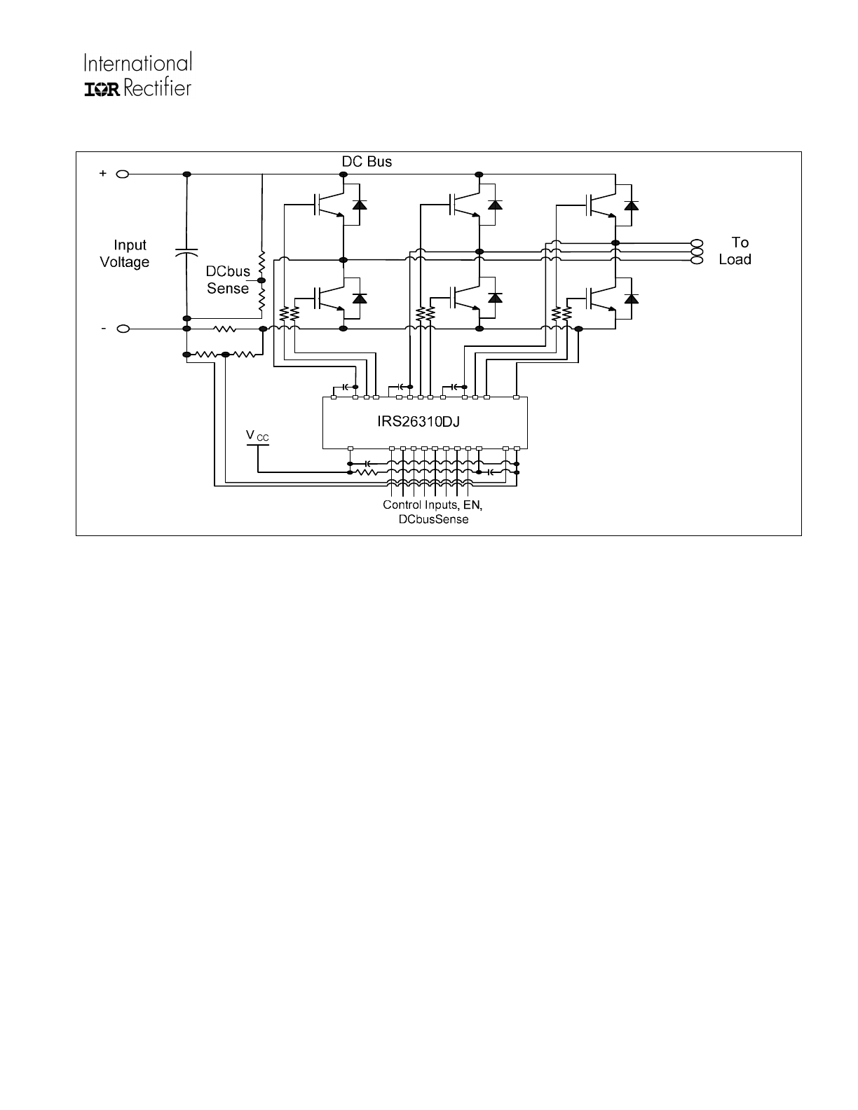
Typical Application Diagram
Not recommended for new designs. For new designs, we recommend 6EDL04I06NT/PT
IRS26310DJPbF
www.irf.com
© 2007 International Rectifier
5
Qualification Information
†
Industrial
††
Qualification Level
Comments: This family of ICs has passed JEDEC’s
Industrial qualification. IR’s Consumer qualification level is
granted by extension of the higher Industrial level.
Moisture Sensitivity Level
PLCC44
MSL3
†††
, 245°C
(per IPC/JEDEC J-STD-020)
Machine Model
Class B
(per JEDEC standard JESD22-A114)
Human Body Model
Class 2
(per EIA/JEDEC standard EIA/JESD22-A115)
ESD
Charged Device Model
Class IV
(per JEDEC standard JESD22-C101)
IC Latch-Up Test
Class I, Level A
(per JESD78)
RoHS Compliant
Yes
†
Qualification standards can be found at International Rectifier’s web site
http://www.irf.com/
†† Higher qualification ratings may be available should the user have such requirements. Please contact your
International Rectifier sales representative for further information.
††† Higher MSL ratings may be available for the specific package types listed here. Please contact your
International Rectifier sales representative for further information.
Not recommended for new designs. For new designs, we recommend 6EDL04I06NT/PT
IRS26310DJPbF
www.irf.com
© 2007 International Rectifier
6
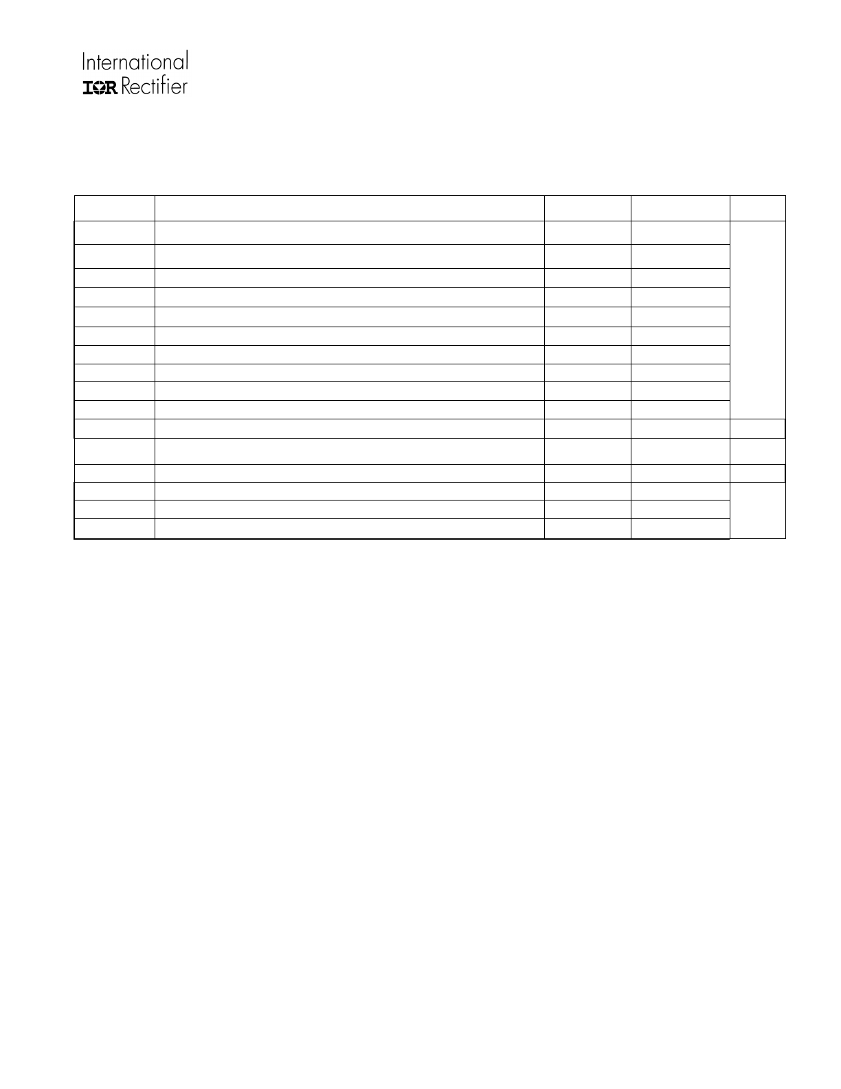
Absolute Maximum Ratings
Absolute maximum ratings indicate sustained limits beyond which damage to the device may occur. All voltage
parameters are absolute voltages referenced to V
SS
unless otherwise stated in the table. The thermal resistance
and power dissipation ratings are measured under board mounted and still air conditions. Voltage clamps are
included between V
CC
& COM (25 V), V
CC
& V
SS
(20 V), and V
B
& V
S
(20 V).
Symbol
Definition
Min.
Max.
Units
V
S
High side offset voltage
V
B
- 20†
V
B
+ 0.3
V
TST
TST Voltage
-0.3
20
V
B
High side floating supply voltage
-0.3
620
V
HO
High side floating output voltage
V
S
- 0.3
V
B
+ 0.3
V
CC
Low side and logic fixed supply voltage
-0.3
20
V
SS
Logic ground
V
CC
- 20
V
CC
+ 0.3
V
LO1,2,3
Low side output voltage
-0.3
V
CC
+ 0.3
V
IN
Input voltage LIN, HIN, ITRIP, EN, RCIN
V
SS
-0.3
V
CC
+ 0.3
V
FLT
FAULT output voltage
V
SS
-0.3
V
CC
+ 0.3
V
DCBusSense
Input sensing for DC
BUS
voltage
V
SS
-0.3
V
CC
+ 0.3
V
dV/dt
Allowable offset voltage slew rate
—
50
V/ns
P
D
Package power dissipation @ TA
≤ +25°C
—
2
W
Rth
JA
Thermal resistance, junction to ambient
—
63
°C/W
T
J
Junction temperature
—
150
T
S
Storage temperature
-55
150
T
L
Lead temperature (soldering, 10 seconds)
—
300
°C
†
All supplies are fully tested at 25 V. An internal 20 V clamp exists for each supply.
Not recommended for new designs. For new designs, we recommend 6EDL04I06NT/PT
IRS26310DJPbF
www.irf.com
© 2007 International Rectifier
7
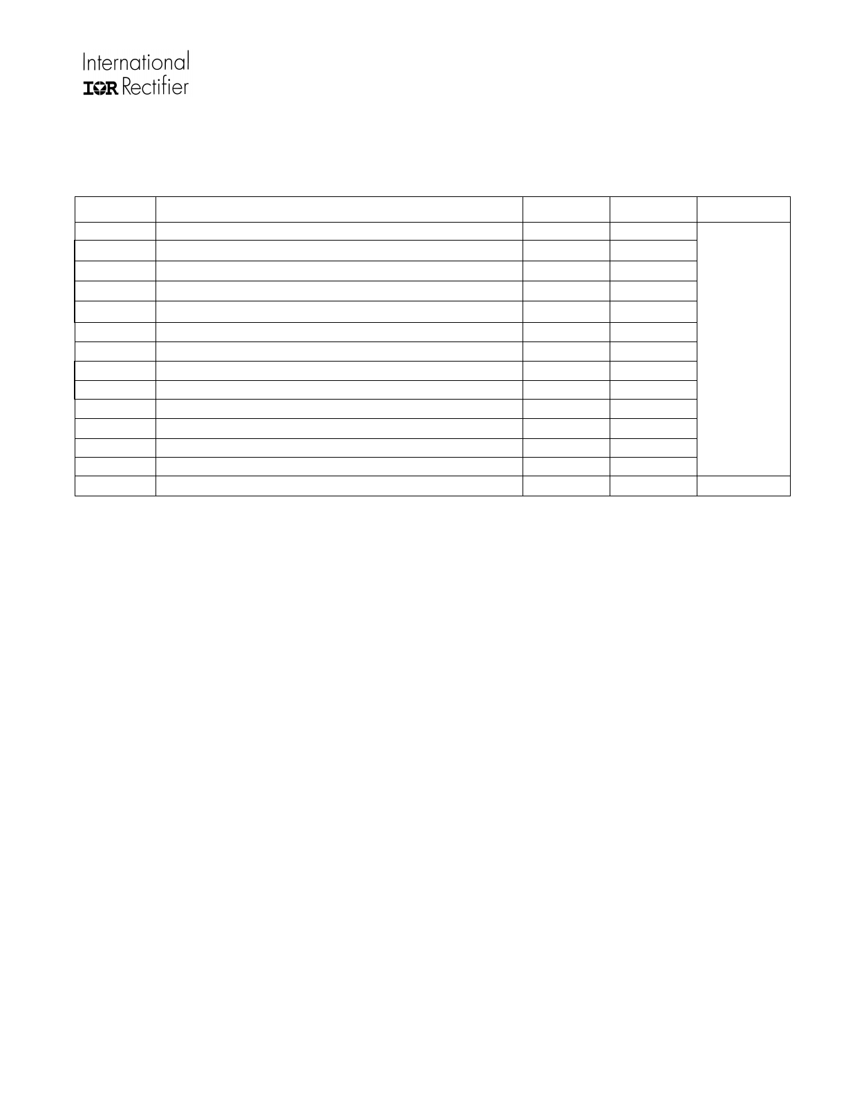
Recommended Operating Conditions
For proper operation, the device should be used within the recommended conditions. All voltage parameters are
absolute voltages referenced to V
SS
unless otherwise stated in the table. The offset rating is tested with supplies
of (V
CC
-COM) = (V
B
-V
S
) = 15 V.
Symbol
Definition
Min.
Max.
Units
V
B
High side floating supply voltage
V
S
+12
V
S
+ 20
V
S
High side floating supply voltage
†
COM-8
600
V
S
(t)
Transient high-side floating supply voltage
††
-50
600
V
TST
TST Voltage
12
20
V
CC
Low side supply voltage
12
20
V
HO
High side output voltage
V
S
V
B
V
LO
Low side output voltage
0
V
CC
V
SS
Logic ground
-5
5
V
FLT
FAULT output voltage
V
SS
V
CC
V
RCIN
RCIN input voltage
V
SS
V
CC
V
ITRIP
ITRIP input voltage
V
SS
V
SS + 5
V
IN
Logic input voltage LIN, HIN, EN
V
SS
V
SS + 5
V
DCBusSense
Input sensing for DCbus voltage†††
V
SS
V
CC
V
T
A
Ambient temperature
-40
125
°C
†
Logic operation for V
S
of –8 V to 600 V. Logic state held for V
S
of –8 V to –V
BS
. Please refer to Design Tip
DT97-3 for more details.
†† Operational for transient negative V
S
of V
SS
- 50 V
with a 50 ns pulse width. Guaranteed by design. Refer to
the Application Information section of this datasheet for more details.
††† DCBusSense pin is internally clamped with a 10.4 V zener diode.
Not recommended for new designs. For new designs, we recommend 6EDL04I06NT/PT
IRS26310DJPbF
www.irf.com
© 2007 International Rectifier
8
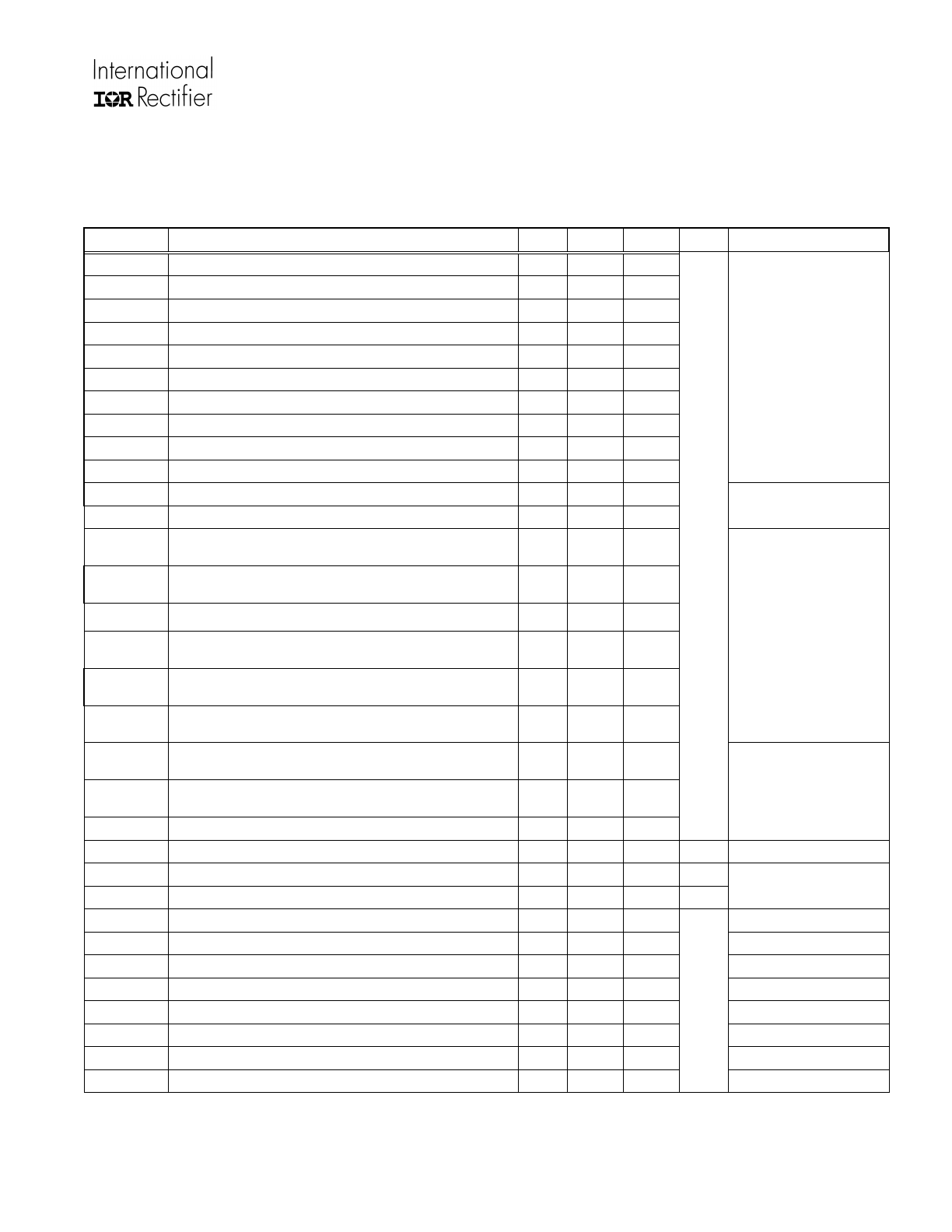
Static Electrical Characteristics
(V
CC
-COM) = (V
B
-V
S
) = 15 V. T
A
= 25
o
C unless otherwise specified. The V
IN
,V
TH
and I
IN
parameters are
referenced to V
SS
and are applicable to all six channels. The V
O
and I
O
parameters are referenced to respective V
S
and COM and are applicable to the respective output leads HO or LO.
The V
CCUV
parameters are referenced to
V
SS
. The V
BSUV
parameters are referenced to V
S
.
Symbol
Definition
Min.
Typ.
Max. Units
Test Conditions
V
IH
Logic “1” input
2.5
—
—
V
IL
Logic “0” input
—
—
0.8
V
IN
,
TH+
Input positive going threshold
—
1.9
—
V
IN
,
TH-
Input negative going threshold
—
1
—
V
EN,TH+
Enable positive going threshold
—
—
2.5
V
EN,TH-
Enable negative going threshold
0.8
—
—
V
IT,TH+
ITRIP positive going threshold
0.37
0.46
0.55
V
IT,HYS
ITRIP hysteresis
0.05
0.07
—
V
RCIN, TH+
RCIN positive going threshold
—
8
—
V
RCIN, HYS
RCIN hysteresis
—
3
—
V
OH
High level output voltage, V
BIAS
– V
O
—
1.12
1.74
V
OL
Low level output voltage, V
O
—
0.4
0.6
I
O
= 20 mA
V
CCUV+
V
CC
supply undervoltage positive going
threshold
10.4
11.1
11.6
V
CCUV-
V
CC
supply undervoltage negative going
threshold
10.2
10.9
11.4
V
CCUVHYS
V
CC
supply undervoltage hysteresis
0.17
0.2
—
V
BSUV+
V
BS
supply undervoltage positive going
threshold
10.4
11.1
11.6
V
BSUV-
V
BS
supply undervoltage negative going
threshold
10.2
10.9
11.4
V
BSUVHY
V
BS
supply undervoltage hysteresis
0.17
0.2
—
V
DCBUSSTH+
Over voltage DCBusSense positive going
threshold
3.86
4.20
4.54
V
DCBUSSTH-
Over voltage DCBusSense negative going
threshold
3.70
4.03
4.35
V
DCBUSSHYS
Over voltage DCBusSense hysteresis
0.14
0.17
—
V
Note 1
I
LK
Offset supply leakage current
—
3
50
V
B
=V
S
= 600 V
I
QBS
Quiescent V
BS
supply current
—
50
120
I
QCC
Quiescent V
CC
supply current
—
3
4
mA
All inputs @ logic 0
value
I
IN+
Input bias current (Lo or Ho= High)
—
100
150
V
IN
= 3.3 V
I
IN-
Input bias current (Lo or Ho = Low)
-1
0
—
V
IN
= 0 V
I
ITRIP+
“High” ITRIP input bias current
—
5
40
V
ITRIP
= 5 V
I
ITRIP-
“Low” ITRIP input bias current
-1
0
—
V
ITRIP
= 0 V
I
FLT/EN+
“High” FLT/ENABLE input bias current
—
0
1
V
FLT/EN
= 3.3 V
I
FLT/EN-
“Low” FLT/ENABLE input bias current
-1
0
—
V
FLT/EN
= 0 V
I
DCBUSSENSE+
“High” DCBusSense input bias current
—
0
1
V
DCBSENSE
= 5 V
I
DCBUSSENSE-
“Low” DCBusSense input bias current
-1
0
—
uA
V
DCBSENSE
= 0 V
Note 1: Guaranteed by design over a temperature range of 0ºC to 110ºC
Not recommended for new designs. For new designs, we recommend 6EDL04I06NT/PT
IRS26310DJPbF
www.irf.com
© 2007 International Rectifier
9
Static Electrical Characteristics (continued)
(V
CC
-COM) = (V
B
-V
S
) = 15 V. T
A
= 25
o
C unless otherwise specified. The V
IN
,V
TH
and I
IN
parameters are referenced
to V
SS
and are applicable to all six channels. The V
O
and I
O
parameters are referenced to respective V
S
and COM and
are applicable to the respective output leads HO or LO.
The V
CCUV
parameters are referenced to V
SS
. The V
BSUV
parameters are referenced to V
S
.
Symbol
Definition
Min.
Typ.
Max. Units
Test
Conditions
I
RCIN+
“High” RCIN input bias current
—
0
1
V
RCIN
= 15 V
I
RCIN-
“Low” RCIN input bias current
-1
0
—
uA
V
RCIN
= 0 V
Io+
Output high short circuit pulsed current
120
200
—
Vo = 0 V,
PW ≤ 10 µs
Io-
Output low short circuit pulsed current
250
350
—
mA
Vo = 15 V,
PW ≤ 10 µs
R
on_RCIN
RCIN low on resistance
—
50
100
R
on_FAULTEN
FAULT low on resistance
—
50
100
I = 1.5 mA
R
BS
Internal bootstrap diode Ron
—
200
400
Ω
Not recommended for new designs. For new designs, we recommend 6EDL04I06NT/PT
IRS26310DJPbF
www.irf.com
© 2008 International Rectifier
10
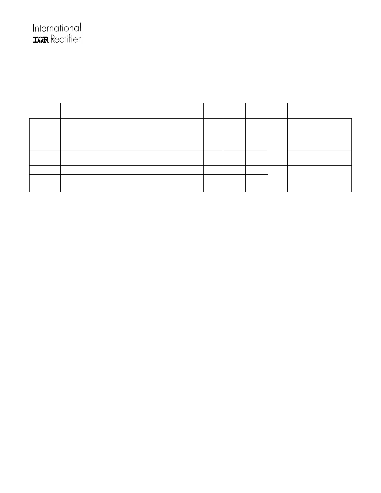
Dynamic Electrical Characteristics
V
CC
= V
B
= 15 V, V
S
= V
SS
= COM, T
A
= 25
o
C, and C
L
= 1000 pF unless otherwise specified.
Symbol
Definition
Min.
Typ.
Max.
Units
Test Conditions
t
on
Turn-on propagation delay
400
530
750
t
off
Turn-off propagation delay
400
530
750
t
r
Turn-on rise time
—
125
190
t
f
Turn-off fall time
—
50
75
V
IN
= 0V & 5V
t
ITRIP
ITRIP to output shutdown
propagation delay
500
750
1200
V
ITRIP
= 5V
t
ITRIP_blk
ITRIP blanking time
—
500
750
t
FLT
ITRIP to FAULT propagation
delay
400
600
950
V
IN
= 0V & 5V
V
ITRIP
= 5V
t
ENOUT
ENABLE high to output
propagation delay
350
460
650
t
SDOUT
ENABLE low to output
shutdown propagation delay
350
460
650
V
IN
= 0V & 5V
V
EN
= 0V & 3.3V
t
ZV
_
DCBS_LOon
DCBusSense entering Over
voltage to LO turn on
310
460
730
t
ZV
_
DCBS_HOoff
DCBusSense entering Over
voltage to HO turn off
310
460
730
t
ZV
_
DCBS_HOon
DCBusSense exiting Over
voltage to HO turn on
270
380
590
t
ZV
_
DCBS_LOoff
DCBusSense exiting Over
voltage to LO turn off
300
450
720
t
ZV_DCBS_flt_LO
DCBusSense input filter time on
LO
140
250
420
t
ZV_DCBS_flt_HO
DC
BUS
S
ENSE
input filter time on
HO
140
250
420
ns
V
DCBSENSE
= 0V & 5V
t
FILIN
Input filter time (HIN, LIN)
†
200
350
510
V
IN
= 0V & 5V
t
FILTEREN
Enable input filter time
100
200
—
DT
Deadtime
190
290
420
MT
Ton, Toff matching time (on all
six channels)
—
—
50
MDT
DT matching (HIN->LO & LO-
>HIN on all channels)
—
—
60
V
IN
= 0V & 5V
External dead time 0s
PM
Pulse width distortion
††
—
—
75
ns
PW input =10µs
t
FLTCLR
FAULT clear time RCIN: R = 2
meg, C = 1nF
1.3
1.65
2
ms
V
IN
= 0V or 5V
V
ITRIP
= 0V
†
The minimum width of the input pulse is recommended to exceed 500 ns to ensure the filtering time of the
input filter is exceeded.
†† PM is defined as PW
IN
- PW
OUT
.
Not recommended for new designs. For new designs, we recommend 6EDL04I06NT/PT