
IRS21953SPBF
Features
•
2 low side output channels sharing common ground
•
1 high side output channel
•
CMOS Schmitt trigger inputs with pull down resistor
•
Under voltage lockout on all channels
•
5 V compatible logic level Inputs
•
Immune to –Vs spike and tolerant to dVs/dt & dVss/dt
•
Shoot through prevention logic
Descriptions
HIGH SIDE & DUAL LOW SIDE
DRIVER IC
Product Summary
V
OFFSET
(low side) -600 V (VSS)
V
OFFSET
(high side) 600 V (COM)
V
OUT
10 V to 20 V
t
on
/t
off
(typ) 380 ns/380 ns
I
o+/-
0.5 A/0.5 A
Package
16-Lead SOIC (narrow body
)
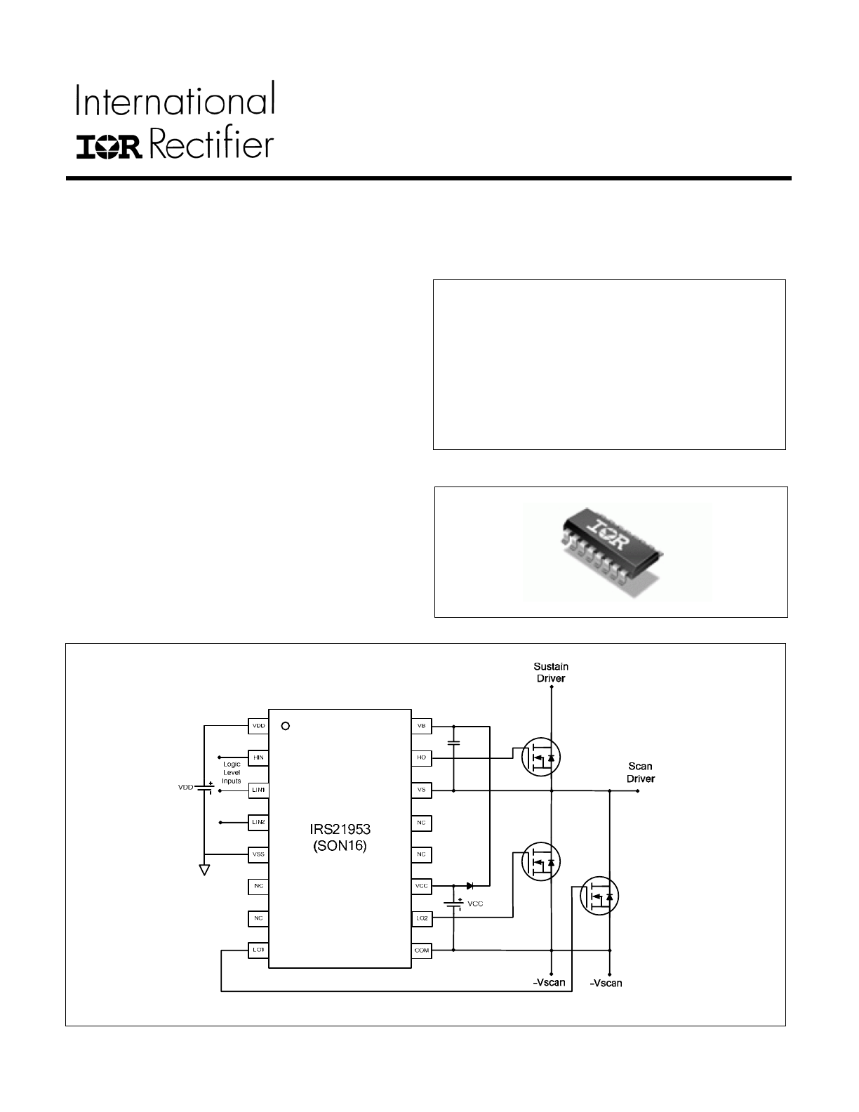
Typical Connection Diagram
The IRS21953 contains 2 low side outputs sharing
common ground and 1 high side output. Low side drivers
can tolerate up to -600 V below input signal (VSS: input
supply return). High side driver can tolerate up to 600 V
above low side ground (COM: low side supply return).
The IRS21953 has better propagation delay and thermal
characteristics compared to a photo-coupler driver. The
logic inputs are compatible with standard CMOS or LSTTL
output. Proprietary HVIC and latch-up immune CMOS
technologies enable ruggedized monolithic construction.
Not recommended for new designs. No replacement is available
IRS21953SPBF
2
Absolute Maximum Ratings
Absolute maximum ratings indicate sustained limits beyond which damage to the device may occur. All voltage
parameters are absolute voltages referenced to COM.
Symbol Definition
Min
Max
Units
HIN
LIN1
LIN2
Floating logic level Input voltage
VSS-0.3
VDD+0.3
VDD
Floating logic input supply voltage
-0.3
625
VSS
Floating logic input supply return voltage
VDD-25
VDD+0.3
VB
High side floating well supply voltage
-0.3
625
VS
High side floating well supply return voltage
VB-25
VB+0.3
HO
High side floating gate drive output voltage
VS-0.3
VB+0.3
VCC
Low side supply voltage
-0.3
25
LO1
LO2
Low side output voltage
-0.3
VCC+0.3
V
dVS/dt
Allowable VS offset transient relative to earth ground
-
50
dVSS/dt
Allowable VSS offset transient relative to earth ground
-
50
V/ns
P
D
Package power dissipation @ T
A
<=+25 ºC
- 1
W
R
θJA
Thermal resistance, junction to ambient
-
100
ºC/W
T
J
Junction temperature
-55
150
T
S
Storage temperature
-55
150
T
L
Lead temperature (soldering, 10 seconds)
-
300
ºC
Recommended Operating Conditions
For proper operation, the device should be used within the recommended conditions. All voltage parameters are absolute
voltages referenced to COM.
Symbol
Definition Min
Max
Units
HIN
LIN1
LIN2
Floating logic level input voltage
VSS
VDD
VDD
Floating logic input supply voltage
VSS+10
VSS+20
VSS
Floating logic input supply return voltage
-5
600
VB
High side floating well supply voltage
VS+10
VS+20
VS
High side floating well supply return voltage
-5
600
HO
High side floating gate drive output voltage
VS
VB
VCC
Low side supply voltage
10
20
LO1
LO2
Low side output voltage
0
VCC
V
T
A
Ambient temperature
-40
125
ºC
Note 1:
Logic operation for V
S
of –5 V to 600 V. Logic state held for V
S
of –5 V to –V
BS
. (Please refer to Design Tip
DT97-3 for more details).
Not recommended for new designs. No replacement is available
IRS21953SPBF
3
Static Electrical Characteristics
(VB-VS)=15 V. The V
IN
, V
IN,TH
, V
BSUV
, V
O
, I
O
and I
IN
parameters are referenced to V
S
. T
A
= 25
o
C unless otherwise
specified.
Symbol Definition Min
Typ
Max
Units
Test
Conditions
V
CCUV+
V
CC
supply undervoltage positive going threshold
7.5 8.6 9.7
V
CCUV-
V
CC
supply undervoltage negative going threshold
7.0 8.2 9.4
V
BSUV+
V
BS
supply undervoltage positive going threshold
7.5 8.6 9.7
V
BSUV-
V
BS
supply undervoltage negative going threshold
7.0 8.2 9.4
V
DDUV+
V
DD
supply undervoltage positive going threshold
7.5 8.6 9.7
V
DDUV-
V
DD
supply undervoltage negative going threshold
7.0 8.2 9.4
V
I
LKVCC
I
LKVBS
Offset supply leakage current – both input well
and output well
--- --- 50
V
B
= V
S
= 600 V
V
CC
= V
COM
= 600 V
I
QBS
Quiescent V
BS
supply current
---
70
140
I
QDD
Quiescent V
DD
supply current
---
100
200
I
QCC
Quiescent V
CC
supply current
---
130
260
µA
VIN = 0 V or 5 V
V
IH
Logic “1” input voltage
3.5
---
---
V
IL
Logic “0” input voltage
---
---
0.6
V
OH
High level output voltage, V
BIAS
-V
O
---
---
0.1
I
o
= 0 A
V
OL
Low level output voltage, V
O
---
---
0.1
V
I
o
= 0 A
I
IN+
Logic “1” input bias current
---
2
10
VIN = 5 V
I
IN-
Logic “0” input bias current
---
---
5
µA
VIN = 0 V
I
o+
Output high short circuit pulsed current
---
0.5
---
V
O
=0 V,V
IN
=0 V,
PW<=10 µs
I
o-
Output low short circuit pulsed current
---
0.5
---
A
V
O
=15 V,V
IN
=5 V,
PW<=10 µs
Not recommended for new designs. No replacement is available
IRS21953SPBF
4
Dynamic Electrical Characteristics (All values are target data)
(VB-VS)= 15 V. C
L
= 1000 pF unless otherwise specified. All parameters are reference to COM. T
A
= 25
o
C unless
otherwise specified.
Symbol Definition Min
Typ
Max
Units Test
Conditions
t
on
Turn-on propagation delay of high
and low side
--- 380 ---
V
SS
=200 V, V
S
=0 V
t
off
Turn-off propagation delay of high
and low side
---
380
---
V
SS
=200 V, V
S
=400 V
t
r
Turn-on rise time of high and low
side
--- 25 70
V
SS
=200 V, V
S
=0 V
t
f
Turn-off fall time of high and low
side
--- 25 70
V
SS
=200 V, V
S
=400 V
MT_on
Turn on propagation delay
matching
--- --- 50
V
SS
=200 V, V
S
=0 V
MT_off
Turn off propagation delay
matching
--- --- 50
ns
V
SS
=200 V, V
S
=400 V
Not recommended for new designs. No replacement is available
IRS21953SPBF
5
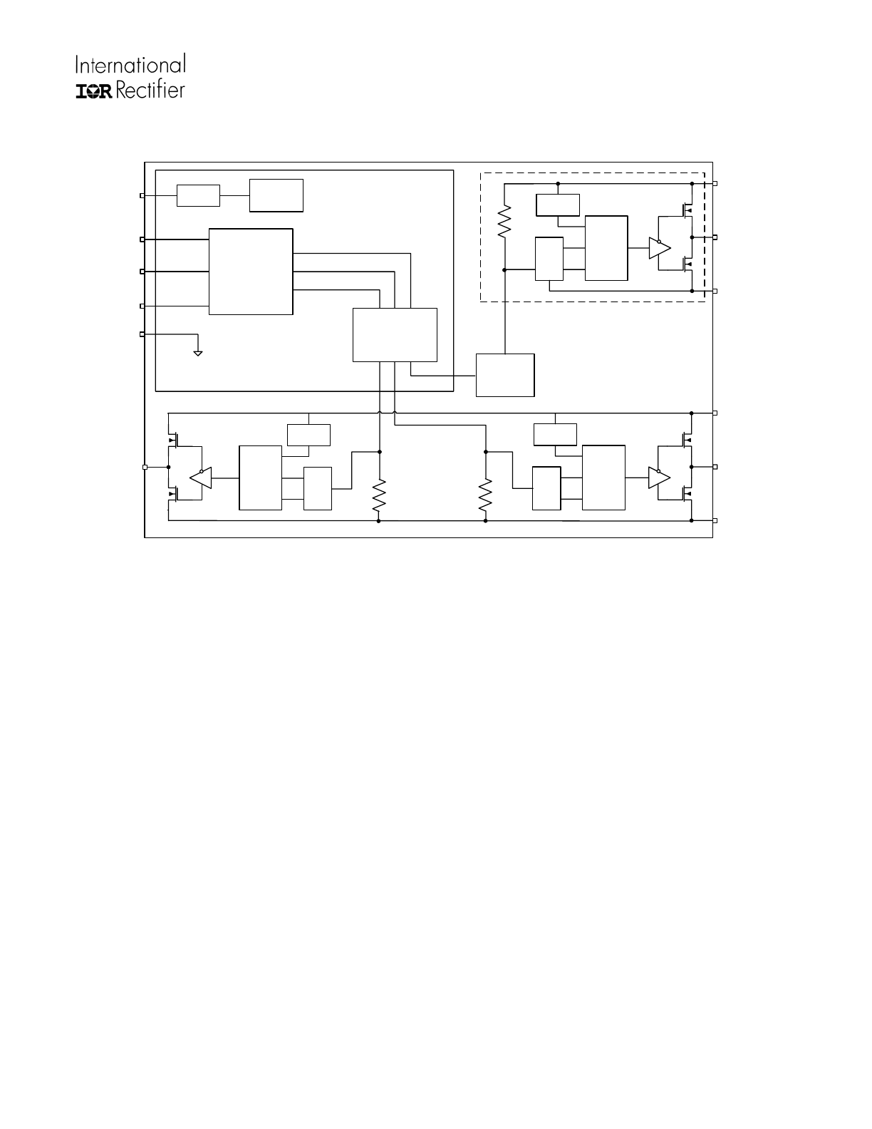
Functional Block Diagram
Level
Shift
Up
R
R Q
S
UVLO
Pulse
Filter
5V
Regulator
Level
Shift
Down
VDD
LIN2
LIN1
HIN
HO
VB
VS
VSS
R
R Q
S
UVLO
Pulse
Filter
VCC
LO2
COM
R
Q R
S
UVLO
Pulse
Filter
LO1
Shoot
Through
Prevention
Logic
UVLO
Not recommended for new designs. No replacement is available
IRS21953SPBF
6
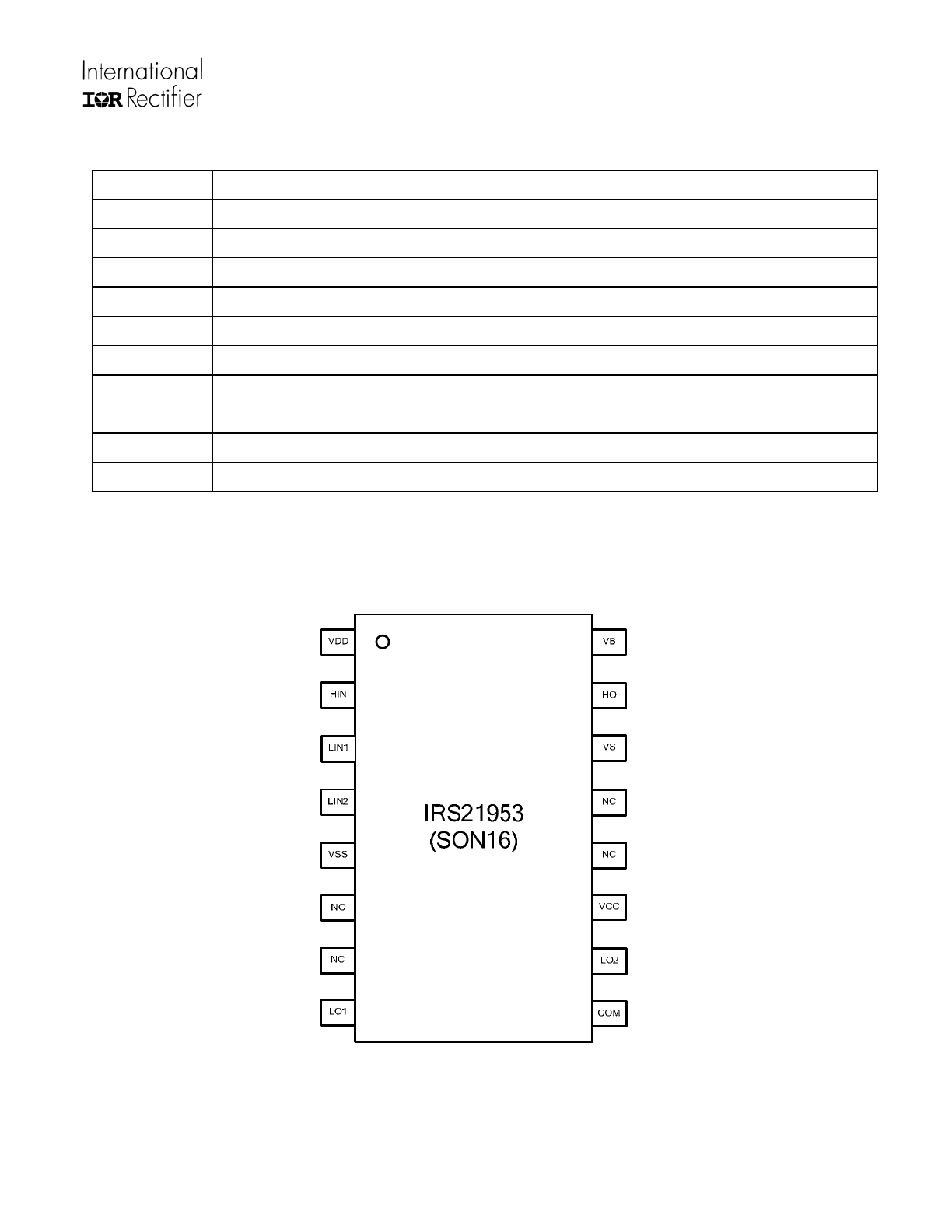
Lead Definitions
Symbol Description
VDD
Input logic supply voltage
HIN
Logic input for high side gate driver
LIN1, LIN2
Logic inputs for low side gate driver
VSS
Input logic supply return
LO1, LO2
Low side outputs
VCC
Low side supply voltage
COM
Low side supply return
HO
High side output
VB
High side floating supply voltage
VS
High side floating supply return
Lead Assignments
Not recommended for new designs. No replacement is available
IRS21953SPBF
7
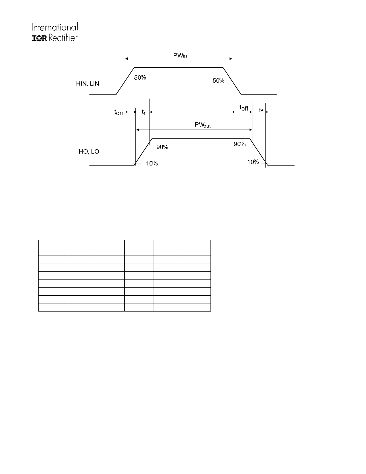
Figure 1: Switching Time Waveforms
Shoot Through Prevention Logic
HIN1 LIN1 LIN2 HO1 LO1 LO2
1 0 0 1 0 0
0 1 0 0 1 0
0 0 1 0 0 1
1 1 0 0 0 0
1 0 1 0 0 0
0 1 1 0 1 1
1 1 1 0 0 0
0 0 0 0 0 0
Not recommended for new designs. No replacement is available
IRS21953SPBF
8
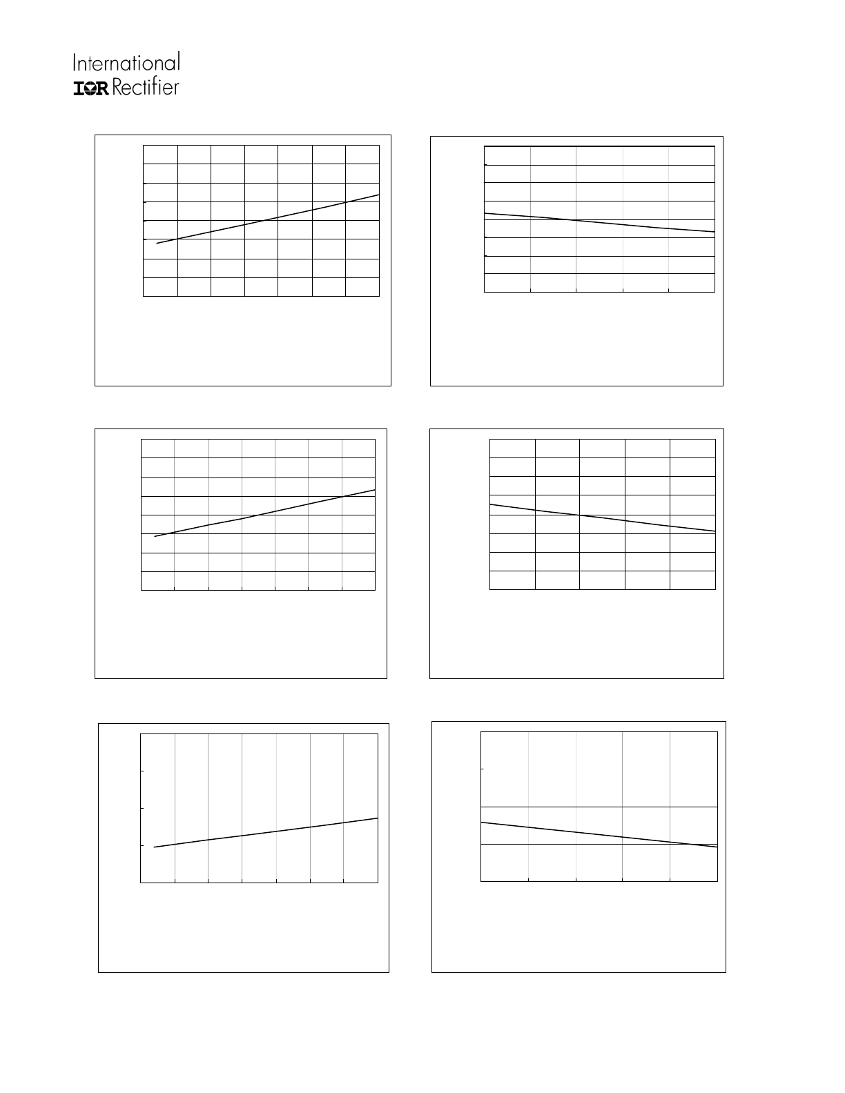
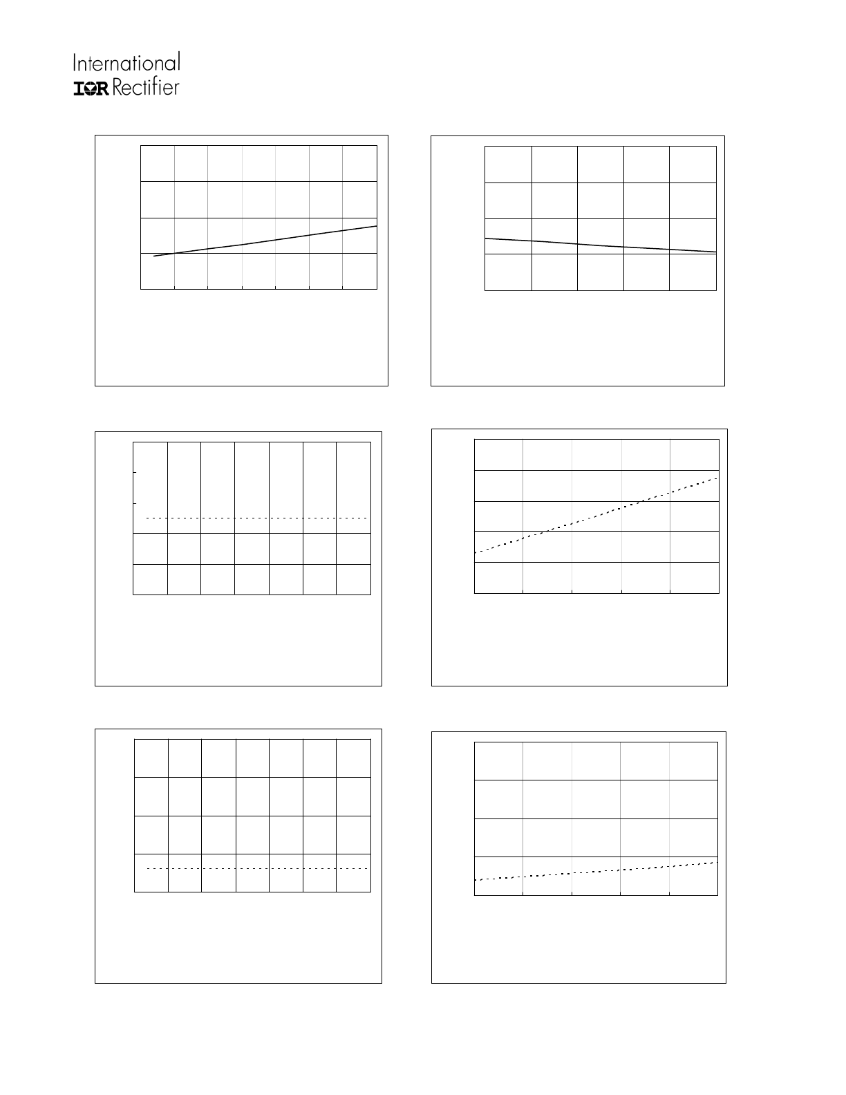
0
100
200
300
400
500
600
700
800
-50
-25
0
25
50
75
100
125
Temperature (
o
C)
Tu
rn
-o
n D
ela
y T
im
e (n
s)
Figure 2A. Turn-On Tim e
vs. Tem perature
Typ.
0
100
200
300
400
500
600
700
800
10
12
14
16
18
20
V
BIAS
Supply Voltage (V)
Tu
rn
-o
n
D
elay
T
im
e (
ns
)
Figure 2B. Turn-On Tim e
vs. Supply Voltage
Typ.
0
100
200
300
400
500
600
700
800
-50
-25
0
25
50
75
100
125
Temperature (
o
C)
Tu
rn
-O
ff T
im
e (
ns
)
Figure 3A. Turn-Off Tim e
vs. Tem perature
Typ.
0
100
200
300
400
500
600
700
800
10
12
14
16
18
20
V
BIAS
Supply Voltage (V)
Tu
rn
-O
ff T
im
e (
ns
)
Figure 3B. Turn-Off Tim e
vs. Supply Voltage
Typ.
0
20
40
60
80
-50
-25
0
25
50
75
100
125
Temperature (
o
C)
Tu
rn
-O
n R
is
e T
im
e (n
s)
Fiure 4A. Turn-On Rise Tim e
vs.Tem perature
Typ.
0
20
40
60
80
10
12
14
16
18
20
V
BIAS
Supply Voltage (V)
Tu
rn
-O
n
R
is
e T
im
e (
ns
)
Figure 4B. Turn-On Rise Tim e
vs. Supply Voltage
Typ.
Not recommended for new designs. No replacement is available
IRS21953SPBF
9
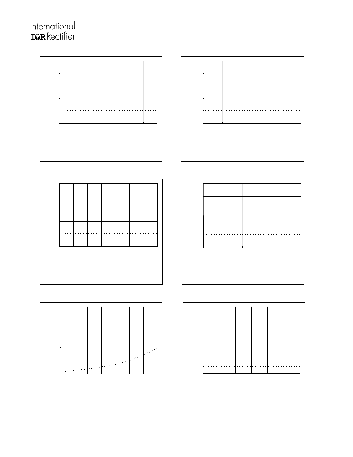
0
20
40
60
80
-50
-25
0
25
50
75
100
125
Temperature (
o
C)
Tu
rn
-O
ff Fa
ll Ti
me
(n
s)
Figure 5A. Turn-Off Fall Tim e
vs. Tem perature
Typ.
0
20
40
60
80
10
12
14
16
18
20
V
BIAS
Supply Voltage (V)
Tu
rn
-O
ff Fa
ll Ti
me
(n
s)
Figure 5B. Turn-Off Fall Tim e
vs. Supply Voltage
Typ.
1
2
3
4
5
6
-50
-25
0
25
50
75
100
125
Temperature (
o
C)
In
pu
t Volt
ag
e (V
)
Figure 6A. Logic "1" Input Voltage
vs. Tem perature
Mi n.
1
2
3
4
5
6
10
12
14
16
18
20
Vcc Supply Voltage (V)
Inpu
t Volt
ag
e (V
)
Figure 6B. Logic "1" Input Voltage
vs. Supply Voltage
Min.
0
1
2
3
4
-50
-25
0
25
50
75
100
125
Temperature (
o
C)
In
pu
t Volt
ag
e (V
)
Figure 7A. Logic "0" Input Voltage
vs. Tem perature
Max.
0
1
2
3
4
10
12
14
16
18
20
V
cc
Supply Voltage (V)
In
pu
t Volt
ag
e (V
)
Figure 7B. Logic "0" Input Voltage
vs. Supply Voltage
Max
Not recommended for new designs. No replacement is available
IRS21953SPBF
10
0.0
0.1
0.2
0.3
0.4
0.5
-50
-25
0
25
50
75
100
125
Temperature (
o
C)
H
igh
L
ev
el O
ut
pu
t Volt
ag
e (V
)
Figure 8A. High Level Output
vs. Tem perature
Max.
0
0.1
0.2
0.3
0.4
0.5
10
12
14
16
18
20
V
cc
Supply Voltage (V)
H
igh
L
ev
el O
ut
pu
t Volt
ag
e (V
)
Figure 8B. High Level Output
vs. Supply Voltage
Max.
0
0.1
0.2
0.3
0.4
0.5
-50
-25
0
25
50
75
100
125
Temperature (
o
C)
Lo
w
Le
ve
l O
ut
pu
t Volt
ag
e (V)
Figure 9A. Low Level Output
vs.Tem perature
Max.
0
0.1
0.2
0.3
0.4
0.5
10
12
14
16
18
20
V
cc
Supply Voltage (V)
Lo
w
Le
ve
l O
ut
pu
t Volt
ag
e (V)
Figure 9B. Low Level Output
vs. Supply Voltage
Max.
0
100
200
300
400
500
-50
-25
0
25
50
75
100
125
Temperature (
o
C)
O
ffs
et
Su
pp
ly
Le
ak
ag
e C
urr
en
t (u
A)
Max.
Figure 10A. Offset Supply Leakage Current
vs. Tem perature
0
100
200
300
400
500
0
100
200
300
400
500
600
V
B
Boost Voltage (V)
O
ffs
et
Su
pp
ly
Le
ak
ag
e C
urr
en
t (u
A)
Max.
Figure 10B. Offset Supply Leakage Current
vs. Supply Voltage
Not recommended for new designs. No replacement is available