
www.irf.com
© 2008 International Rectifier
1
January 16, 2009
Datasheet No. - PD97376
IRS21856S
High(Dual Mode) and Low Side Driver
Features
•
High side Programmable ramp gate drive
•
High side generic gate driver integrated using the
same high side output pin
•
Low side generic gate driver
•
Under voltage lockout for VCC & VBS
•
5V input logic compatible
•
Tolerant to negative transient voltage on VS
•
Shoot through prevention
• RoHS
compliant
Product Summary
Topology PDP
V
OFFSET
≤ 600 V
HO1 SR+
4.5V/us
I
o+
& I
o-
(typical)
0.5A & 0.5A
t
ON
& t
OFF
(typical)
160ns & 160ns
Package Options
14-Lead SOIC (narrow body
)
Not recommended for new designs. No replacement is available
IRS21856S
www.irf.com
© 2008 International Rectifier
2
Table of Contents
Page
Description
3
Simplified Block Diagram
4
Typical Application Diagram
5
Qualification Information
7
Absolute Maximum Ratings
8
Recommended Operating Conditions
8
Static Electrical Characteristics
9
DV / Linear (Stepwise) Mode
10
Dynamic Electrical Characteristics
10
Timing Diagram and logic truth table
11
Input/Output Pin Equivalent Circuit Diagram
16
Lead Definitions
17
Lead Assignments
17
Package Details
18
Tape and Reel Details
19
Part Marking Information
20
Ordering information
21
Not recommended for new designs. No replacement is available

IRS21856S
www.irf.com
© 2008 International Rectifier
3
Description
The IRS21856 is high voltage and programmable ramp slope control gate driver for MOSFET and IGBT with
single high side dual mode driver and low side driver. Proprietary HVIC and latch immune CMOS
technologies enable ruggedized monolithic construction. The logic input is compatible with 5V standard
CMOS or LSTTL output. The output driver features a programmable slope control by external R/C and input
signal. The floating channels can be used to drive an N-channel power MOSFET or IGBT in the high side
configuration, which operates up to 600 volts above the COM ground.
Not recommended for new designs. No replacement is available
IRS21856S
www.irf.com
© 2008 International Rectifier
4
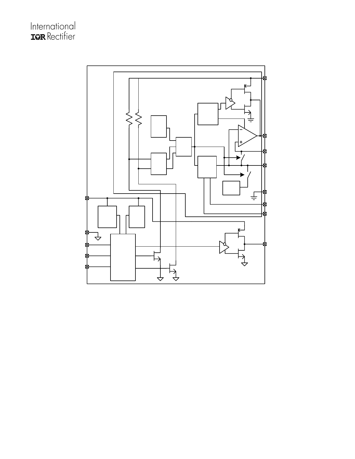
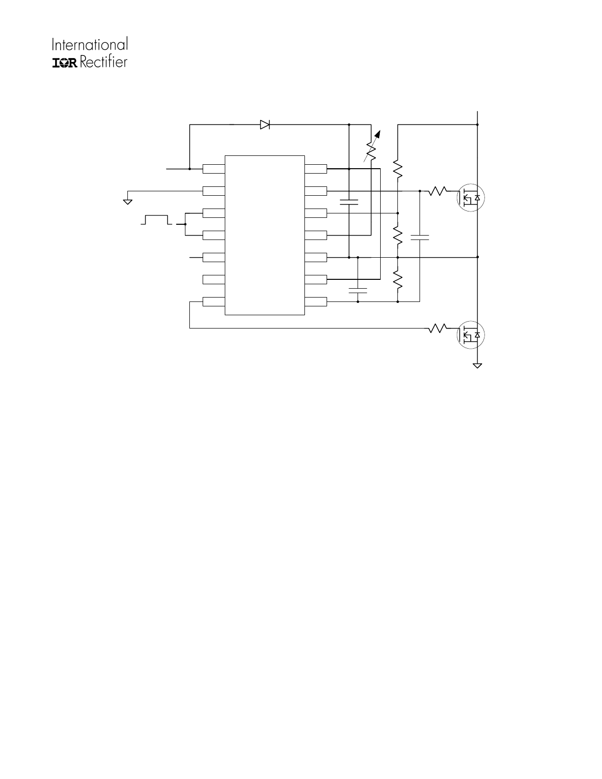
Simplified Block Diagram
UVLO
5V
Regulator
Logic
&
Pulse
Generator
UVLO
Pulse
Filter
10V
Regulator
Conditioning
& OPAMP
Driving
Reference
Generating
R
R
S
VB
HO1
VSE
VREF
VS
DV
RES
LO3
LIN3
HIN2
HIN1
COM
VCC
Not recommended for new designs. No replacement is available
IRS21856S
www.irf.com
© 2008 International Rectifier
5
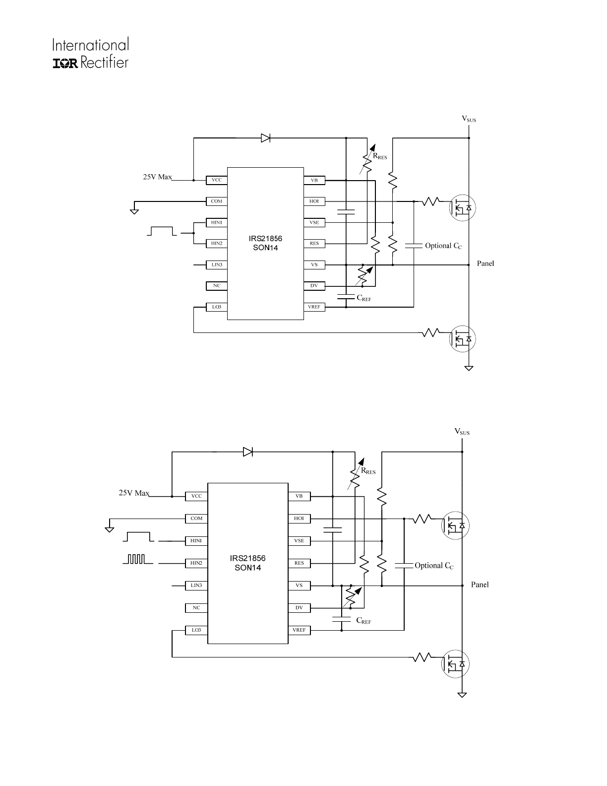
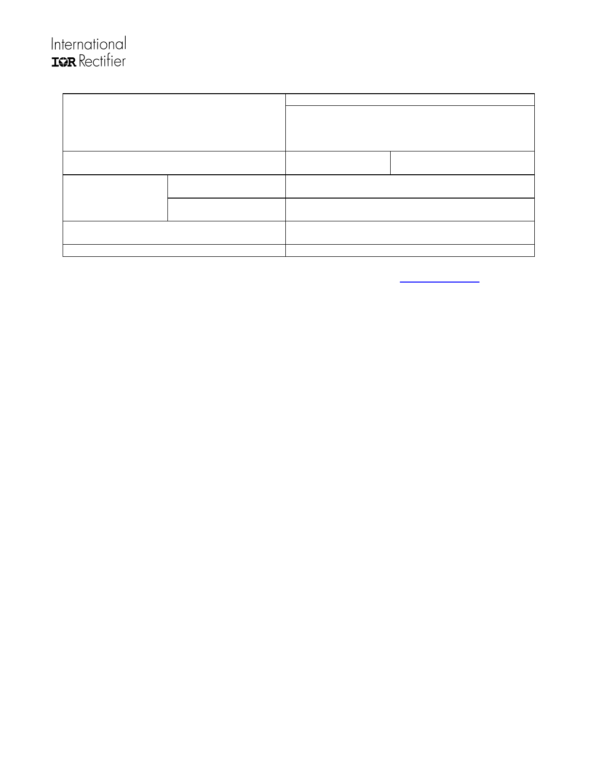
Typical Connection Diagrams
A) Linear Ramp driver’s connection diagram
B) Stepwise Linear Ramp driver’s connection diagram
Not recommended for new designs. No replacement is available
IRS21856S
www.irf.com
© 2008 International Rectifier
6
C) Exponential Ramp driver’s connection diagram
IRS21856
SON14
VB
HO1
VSE
RES
VS
DV
VREF
VCC
COM
HIN1
HIN2
LIN3
NC
LO3
Optional C
C
C
REF
R
RES
25V Max
V
SUS
Panel
R
REF
Not recommended for new designs. No replacement is available
IRS21856S
www.irf.com
© 2008 International Rectifier
7
Qualification Information
†
Industrial
††
Qualification Level
Comments: This family of ICs has passed JEDEC’s
Industrial qualification. IR’s Consumer qualification
level is granted by extension of the higher Industrial
level.
Moisture Sensitivity Level
SOIC14N
MSL2
†††
260°C
(per IPC/JEDEC J-STD-020)
Machine Model
Class A
(per JEDEC standard JESD22-A115)
ESD
Human Body Model
Class 2
(per EIA/JEDEC standard EIA/JESD22-A114)
IC Latch-Up Test
Class I , Level A
(per JESD78)
RoHS Compliant
Yes
† Qualification standards can be found at International Rectifier’s web site
http://www.irf.com/
†† Higher qualification ratings may be available should the user have such requirements. Please contact
your International Rectifier sales representative for further information.
††† Higher MSL ratings may be available for the specific package types listed here. Please contact your
International Rectifier sales representative for further information.
Not recommended for new designs. No replacement is available
IRS21856S
www.irf.com
© 2008 International Rectifier
8
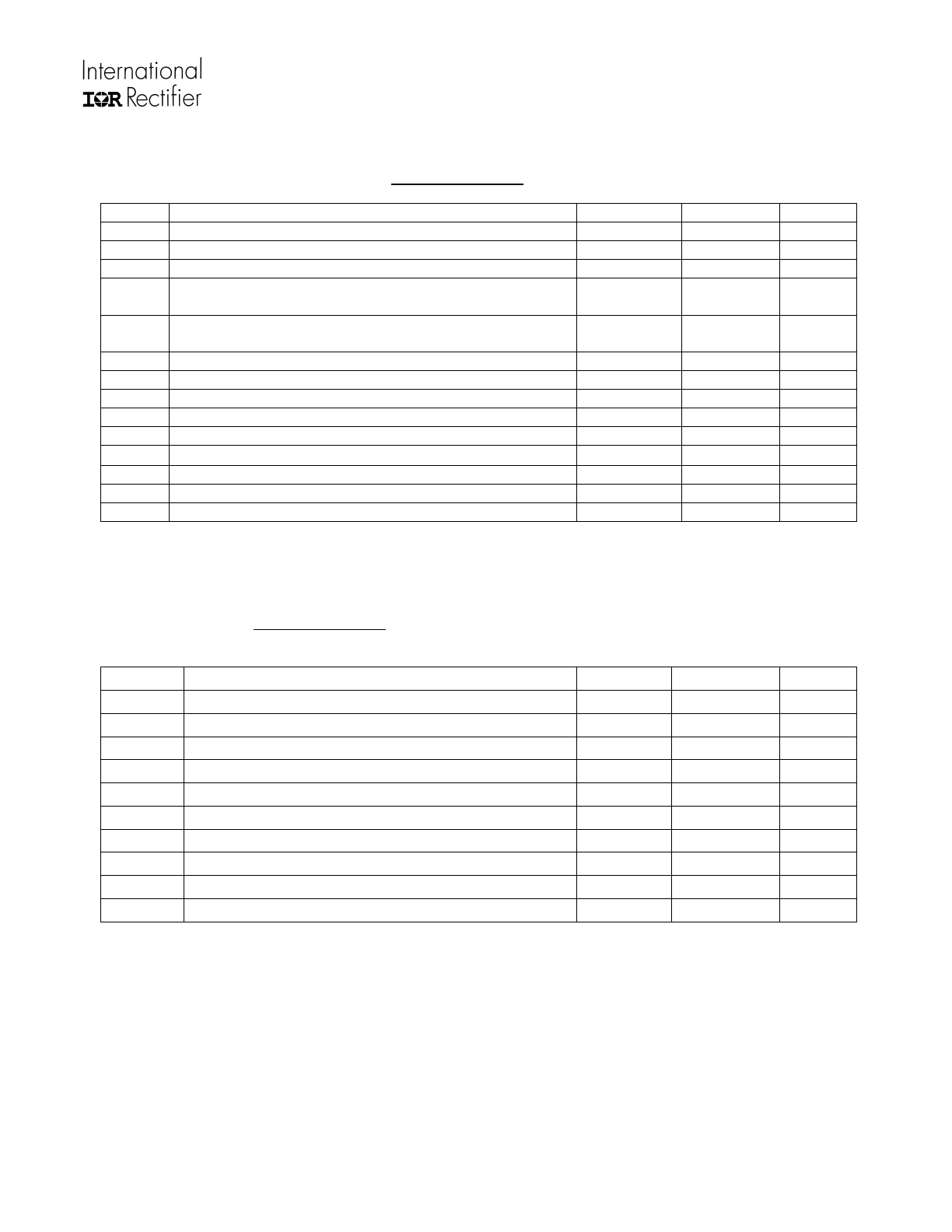
Absolute Maximum Ratings
Absolute maximum ratings indicate sustained limits beyond which damage to the device may occur. All
voltage parameters are absolute voltages referenced to COM.
Symbol Definition
Min
Max
Units
V
CC
Low side supply voltage
-0.3
25
V
V
IN
Logic input voltage (HIN1, HIN2, LIN3)
COM-0.3
VCC +0.3
V
V
LO
Low side gate drive output voltage
COM-0.3
VCC +0.3
V
V
DV
,
V
VREF
High side inputs voltage
VS-0.3
VB+0.3
V
V
VSE
,
V
RES
High side inputs voltage
VS-0.3
VB+0.3
V
V
B
High side floating well supply voltage
-0.3
625
V
V
S
High side floating well supply return voltage
VB-25
VB+0.3
V
V
HO1
Floating gate drive output voltage
VS-0.3
VB+0.3
V
dV
S
/dt Allowable VS offset supply transient relative to COM
-
50
V/ns
P
D
Package Power Dissipation @ TA<=+25ºC
-
1.0
W
R
θJA
Thermal Resistance, Junction to Ambient
-
120
ºC/W
T
J
Junction
Temperature
-55
150
ºC
T
S
Storage
Temperature
-55
150
ºC
T
L
Lead temperature (Soldering, 10 seconds)
-
300
ºC
Recommended Operating Conditions
For proper operation, the device should be used within the recommended conditions. All voltage parameters
are absolute voltages referenced to COM. The offset rating are tested with supplies of (VCC-COM) = (VB-
VS)=15V.
Symbol Definition
Min
Max
Units
V
CC
Low side supply voltage
10
20
V
V
IN
HIN1, HIN2, LIN3 input voltage
COM
V
CC
V
V
LO3
Low side gate drive output voltage
COM
V
CC
V
V
B
High side floating well supply voltage
V
S
+10 V
S
+20 V
V
RES
RES input voltage
V
S
V
B
V
V
DV
DV input voltage
V
S
V
B
V
V
VREF, VSE
VREF and VSE input voltage
V
S
V
B
-3
V
V
S
High side floating well supply offset voltage
Note2††
600 V
V
HO1
Floating gate drive output voltage
V
S
V
B
V
T
A
Ambient Temperature
-40
125
ºC
†
V
S
and V
B
voltages will be tolerant to short negative transient spikes. These will be defined and
specified in the future.
††
Logic operation for Vs of -5 to 600V. Logic state held for Vs of -5V to –V
BS
. (Please refer to Design Tip
DT97-3 for more details).
Not recommended for new designs. No replacement is available
IRS21856S
www.irf.com
© 2008 International Rectifier
9
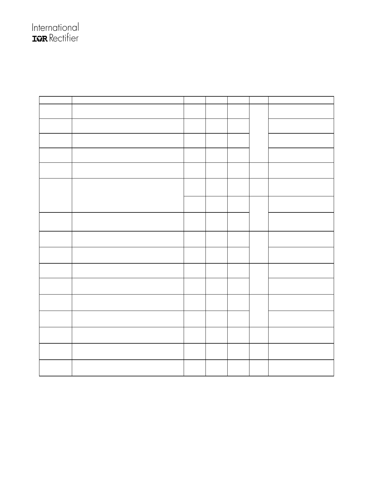
Static Electrical Characteristics
(VCC-COM) = (VB-VS)=15V.
TA = 25ºC. The V
IN
, V
IN TH
and I
IN
parameters are referenced to COM. The V
O
and I
O
parameters are referenced to respective VS, COM and are applicable to the respective output leads
HO1, LO3.
The V
CCUV
parameters are referenced to COM. The V
BSUV
parameters are referenced to V
S
.
Symbol
Definition
Min Typ Max
Units Test
Conditions
V
CCUV+
V
CC
supply undervoltage positive going
threshold
8.1 9.0 9.9
V
CCUV-
V
CC
supply undervoltage negative
going threshold
7.5 8.3 9.1
V
BSUV+
V
BS
supply undervoltage positive going
threshold
8.1 9.0 9.9
V
BSUV-
V
BS
supply undervoltage negative
going threshold
7.5 8.3 9.1
V
I
LK
High side floating well offset supply
leakage current
--- --- 50
µA
V
B
= V
S
= 600V
--- 4.7 8.5
mA
IN1, 2 = 5V,
RES=130kohm
I
QBS
Quiescent VBS supply current
--- 800 1400
IN1, 2 = 0V,
RES=130kohm
I
QCC
Quiescent VCC supply current
---
120
250
µA
IN1,2,3 = 0V or 5V
V
IH
Logic “1” input voltage
3.5
--- ---
V
IL
Logic “0” input voltage
---
---
0.8
V
I
IN
+
Logic “1” input bias current
---
5
---
V
IN
=5V
I
IN
-
Logic “0” input bias current
---
0
---
µA
V
IN
=0V
Io+_
HO1,LO3
Output high short circuit pulsed current
--- 0.5 ---
V
O
=15V,V
IN
=5V,
PW<=10us
Io-_
HO1,LO3
Output low short circuit pulsed current
--- 0.5 ---
A
V
O
=0V,V
IN
=0V,
PW<=10us
V
OL
_
HO1, LO3
Low level output voltage
---
35
150
mV
Io=2mA
V
OH
_
HO1, LO3
High level output voltage, Vbias-Vo
---
15
80
mV
Io=2mA
DV exp+
Positive DV input threshold for
exponential ramp
--- 9.5 --- V
C
REF
=1nF, V
SE
open
R
RES
=130K
Not recommended for new designs. No replacement is available
IRS21856S
www.irf.com
© 2008 International Rectifier
10
DV / Linear (Stepwise) Mode
Symbol Definition Min
Typ
Max
Units
Test
Conditions
0.4 0.5 0.6
DV=500mV, C
REF
=1nF,
V
SE
open R
RES
=130K,
VREF,
hold
DV reference voltage
2.82 3 3.18
V
DV=3V, C
REF
=1nF, V
SE
open R
RES
=130K,
Dynamic Electrical Characteristics
(VCC-COM)= (VB-VS)=15V. TA = 25ºC. C
L
= 1000pF unless otherwise specified. All parameters are
reference to COM.
Symbol Definition Min
Typ
Max
Units
Test
Conditions
Internal Operational Amplifier Characteristics
t
ref_ln_ramp
Linear ramp reference 10% to
90%
110 170 230 µs
C
REF
=1nF, V
SE
open, R
RES
=130K,
V
DV
=VS=COM
Gm OTA
transconductance
--- 12 --- mS
CL_LO=1nF, V
DV
=V
B,
R
RES
=130K, dc bias 5V
G
open loop
Open loop gain
45
60
---
dB
Cc =1nF, V
DV
=V
B,
R
RES
=130K
BW
SS
Small signal bandwidth
---
3.5
---
MHz
Cc =1nF V
DV
=V
B,
R
RES
=130K
V
OS
Input offset voltage
---
10
---
mV
V
DV
=V
B,
R
RES
=130K
HO1
SR+
Output positive slew rate
---
4.5
---
V/µs
CL_HO1=1nF, V
DV
=V
B,
R
RES
=130K
CMRR
Common mode rejection ratio
55
65
---
dB
V
DV
=V
B,
R
RES
=130K
PSRR
Power supply rejection ratio
55
65
---
dB
V
DV
=V
B,
R
RES
=130K
Propagation Delay Characteristics
t
on
Turn-on delay (HO1, LO3)
---
150
250
t
off
Turn-off delay (HO1, LO3)
---
160
260
t
r
Turn-on rise from 10% to 90%
---
30
70
t
f
Turn-off fall from 90% to 10%
---
20
70
MT
Delay matching, HO1 & LO3 turn-
on/off
50
ns
Gate Drive Mode
C
L
=1nF
Not recommended for new designs. No replacement is available