
Features
•
Gate drive supply range from 10 V to 20 V
•
Undervoltage lockout for V
BS
and V
CC
•
3.3 V and 5 V input logic compatible
•
Tolerant to negative transient voltage
•
Matched propagation delays for all channels
Description
The IRS21851 is a high voltage, high speed power
MOSFET and IGBT single high-side driver with propa-
gation delay matched output channels. Proprietary
HVIC and latch immune CMOS technologies enable
ruggedized monolithic construction. The floating logic
input is compatible with standard CMOS or LSTTL
output, down to 3.3 V logic and can be operated up to
600 V above the ground. The output driver features a
high pulse current buffer stage designed for mini-
mum driver cross-conduction. The floating channel
can be used to drive an N-channel power MOSFET
or IGBT in the high- side configuration, which oper-
ates up to 600 V.
SINGLE HIGH SIDE DRIVER IC
Product Summary
V
OFFSET
600 V max.
I
O
+/-
4 A / 4 A
V
OUT
10 V - 20 V
t
on/off
(typ.)
160 ns & 160 ns
Package
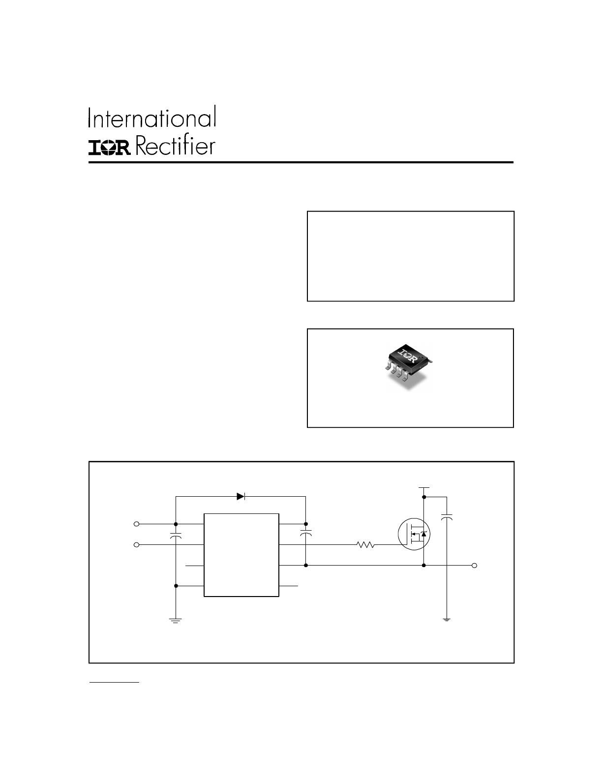
Typical Connection
8-Lead SOIC
IRS21851
IRS21851SPbF
www.irf.com
1
(Refer to Lead Assignments for correct pin configuration). This diagram shows electrical connections only.
Please refer to our Application Notes and DesignTips for proper circuit board layout.
V
CC
V
B
V
S
HO
IN
COM
up to 600V
V
CC
IN
TO
LOAD
•
RoHS compliant
Data Sheet PD No. 60255 revA
Not recommended for new designs. No replacement is available
www.irf.com
2
IRS21851SPbF
Absolute Maximum Ratings
Absolute maximum ratings indicate sustained limits beyond which damage to the device may occur. All voltage parameters
are absolute voltages referenced to COM. The thermal resistance and power dissipation ratings are measured under board
mounted and still air conditions.
Symbol
Definition
Min.
Max.
Units
V
CC
Low-side supply voltage
10
20
V
IN
HIN input voltage
COM
V
CC
V
B
High-side floating well supply voltage
V
S
+ 10
V
S
+ 20
V
S
High-side floating well supply offset voltage
Note 2
600
V
HO
Floating gate drive output voltage
V
S
V
B
T
A
Ambient temperature
-40
125
°C
Note 2: Logic operational for V
S
of -5 V to 600 V. Logic state held for V
S
of -5 V to -V
BS
. (Please refer to the Design
Tip DT97-3 for more details).
Recommended Operating Conditions
For proper operation, the device should be used within the recommended conditions. All voltage parameters are absolute
voltages referenced to COM. The offset rating are tested with supplies of (V
CC
-COM)=(V
B
-V
S
)=15 V.
V
Symbol
Definition
Min.
Max.
Units
V
CC
Low-side supply voltage
-0.3
20 (Note 1)
V
IN
Logic input voltage (HIN)
COM -0.3
V
CC
+ 0.3
V
B
High-side floating well supply voltage
-0.3
620 (Note 1)
V
S
High-side floating well supply return voltage
V
B
- 20
V
B
+ 0.3
V
HO
Floating gate drive output voltage
V
S
- 0.3
V
B
+ 0.3
dV
s
/dt
Allowable V
S
offset supply transient relative to COM
—
50
V/ns
P
D
Package power dissipation @ T
A
≤
+25 °C
—
1.25
W
Rth
JA
Thermal resistance, junction to ambient
—
100
°C/W
T
J
Junction temperature
-55
150
T
S
Storage temperature
-55
150
T
L
Lead temperature (soldering, 10 seconds)
—
300
V
°C
Note 1: All supplies are fully tested at 25 V. An internal 20 V clamp exists for each supply.
Not recommended for new designs. No replacement is available
www.irf.com
3
IRS21851SPbF
Dynamic Electrical Characteristics
(V
CC
-COM)=(V
B
-V
S
)=15 V, T
A
= 25
o
C. C
L
= 1000 pF unless otherwise specified. All parameters are referenced to COM.
Symbol
Definition
Min. Typ. Max. Units Test Conditions
t
on
Turn-on propagation delay
—
160
210
(V
S
-COM) = 0 V
t
off
Turn-off propagation delay
—
160
210
(V
S
-COM)
= 600 V
t
r
Turn-on rise time
—
15
40
t
f
Turn-off fall time
—
15
40
ns
Symbol
Definition
Min. Typ. Max. Units Test Conditions
V
CCUV+
V
CC
supply undervoltage positive going threshold
8.0
8.9
9.8
V
CCUV-
V
CC
supply undervoltage negative going threshold
7.4
8.2
9.0
V
BSUV+
V
BS
supply undervoltage positive going threshold
8.0
8.9
9.8
V
BSUV-
V
BS
supply undervoltage negative going threshold
7.4
8.2
9.0
I
LK
High-side floating well offset supply leakage current —
—
50
V
B
= V
S
= 600 V
I
QBS
Quiescent V
BS
supply current
—
80
150
I
QCC
Quiescent V
CC
supply current
—
120
240
V
IH
Logic “1” input voltage
2.5
—
—
V
IL
Logic “0” input voltage
—
—
0.8
V
OH, HO
HO high level output voltage, V
BIAS
- V
O
—
20
60
V
OL, HO
HO low level output voltage, V
O
—
10
30
I
IN+
Logic “1” input bias current
—
10
20
V
HIN
= 5 V
I
IN-
Logic “0” input bias current
—
0
5
V
HIN
= 0 V
I
O+, HO
Output high short circuit pulsed current HO
—
4
—
V
O
= 0 V, V
IN
= 0 V
PW
≤
10 µs
I
O-, HO
Output low short circuit pulsed current HO
—
4
—
V
O
= 15 V, V
IN
= 15 V
PW
≤
10 µs
Static Electrical Characteristics
(V
CC
-COM)=(V
B
-V
S
)=15 V. The V
IN
, V
TH,
and I
IN
parameters are referenced to COM. The V
O
and I
O
parameters are
referenced respective V
S
and are applicale to the respective output leads HO. The V
CC
parameters are referenced to
COM. The V
BSUV
parameters are referenced to V
S.
V
mV
µA
µA
A
I
O
= 2 mA
HIN
= 0 V or 5 V
V
Not recommended for new designs. No replacement is available
www.irf.com
4
IRS21851
SPbF
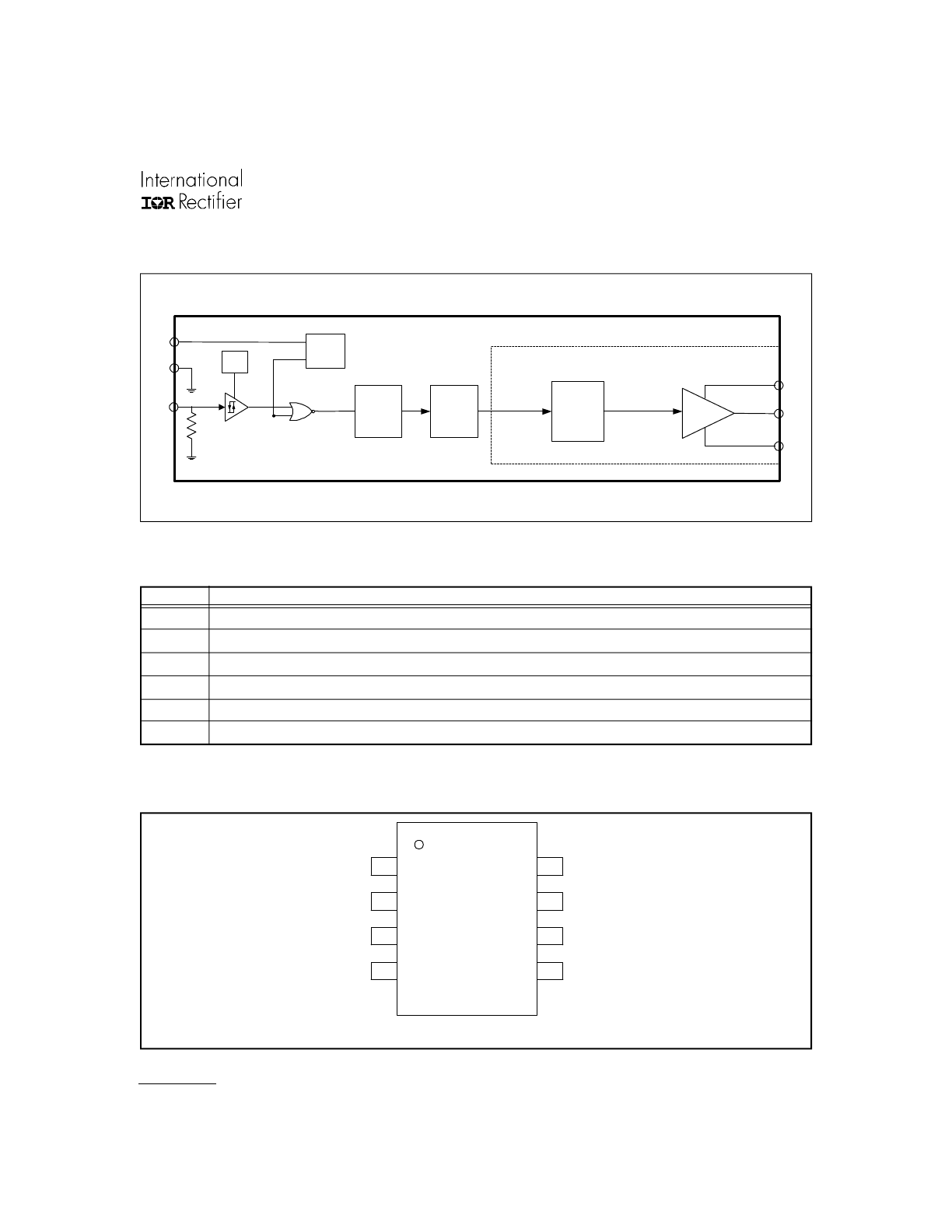
Lead Assignments
Functional Block Diagram
Lead Definitions
Symbol
Description
V
CC
Low-side supply voltage
COM
Ground
V
B
High-side drive floating supply
HO
High-side driver outputs
V
S
High voltage floating supply return
HIN
Logic inputs for high-side gate driver output (in phase)
8-Lead SOIC
1
2
3
4
8
7
6
5
VCC
COM
HIN
VB
HO
VS
IRS21851
S
HIN
LEVEL
SHIFT UP
FILTER,
LATCH
UV DETECT
DRIVER
VB
VS
HO
HIGHSIDE CHANNLE1
PULSE
GEN
VCC
COM
VCCUV
DETECT
5V
VREG
Not recommended for new designs. No replacement is available
www.irf.com
5
IRS21851PbF
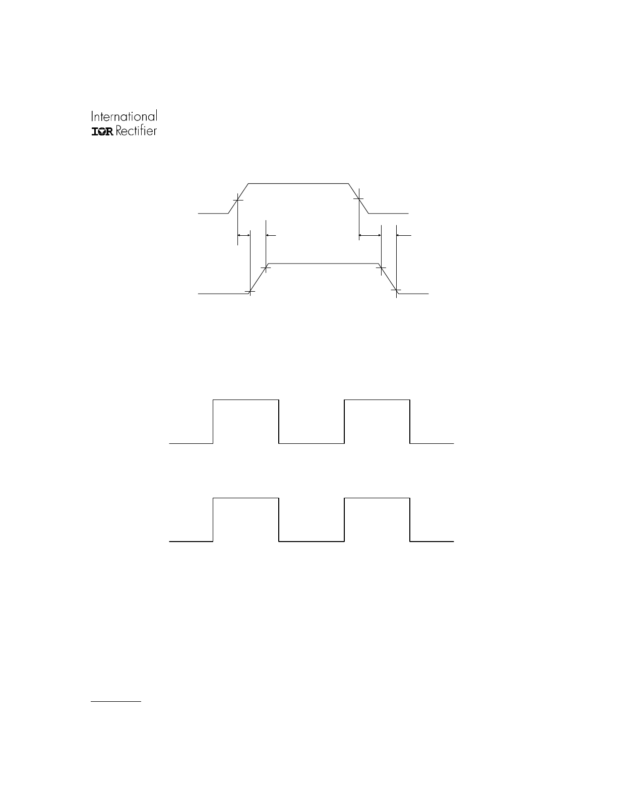
Figure 1. Switching Time Waveforms
Figure 2. Input/Output Timing Diagram
IN
OUT
t
r
50%
90%
10%
50%
90%
10%
t
off
t
f
t
on
HO
HIN
Not recommended for new designs. No replacement is available
www.irf.com
6
IRS21851SPbF
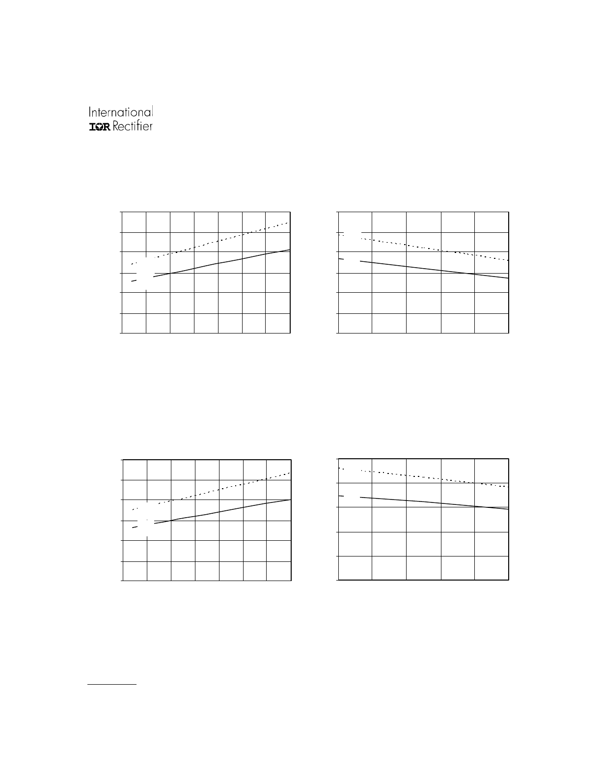
Typ
Max
0
50
100
150
200
250
300
-50
-25
0
25
50
75
100
125
Temperature (°C)
T
u
r
n
-
O
n
P
r
o
p
a
g
a
t
i
o
n
D
e
l
a
y
(
n
s
)
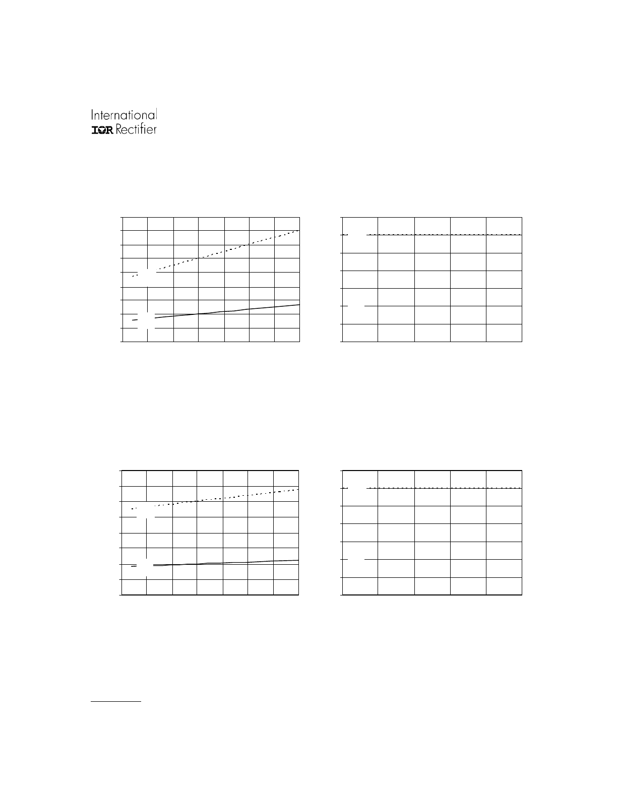
Figure 3A. Turn-On Propagation Delay vs .
Temperature
Typ
Max
0
50
100
150
200
250
300
10
12
14
16
18
20
Supply Voltage (V)
Figure 3B. Turn-On Propagation Delay vs.
Supply Voltage
Typ
Max
0
50
100
150
200
250
300
-50
-25
0
25
50
75
100
125
Temperature (°C)
Tu
rn
-O
ff
Pr
op
ag
at
io
n
D
el
ay
(n
s)
Figure 4A. Turn-Off Propagation Delay vs .
Temperature
Typ
Max
0
50
100
150
200
250
10
12
14
16
18
20
Supply Voltage (V)
T
u
r
n
-
O
f
f P
r
o
p
a
g
a
t
i
o
n
D
e
l
a
y
(
n
s
)
Figure 4B. Turn-Off Propagation Delay vs.
Supply Voltage
T
u
r
n
-
O
n
P
r
o
p
a
g
a
t
i
o
n
D
e
l
a
y
(
n
s
)
Not recommended for new designs. No replacement is available
www.irf.com
7
IRS21851SPbF
Typ
Max
0
5
10
15
20
25
30
35
40
45
-50
-25
0
25
50
75
100
125
Temperature (°C)
T
u
r
n
-
O
n
R
i
s
e
T
i
m
e
(
n
s
)
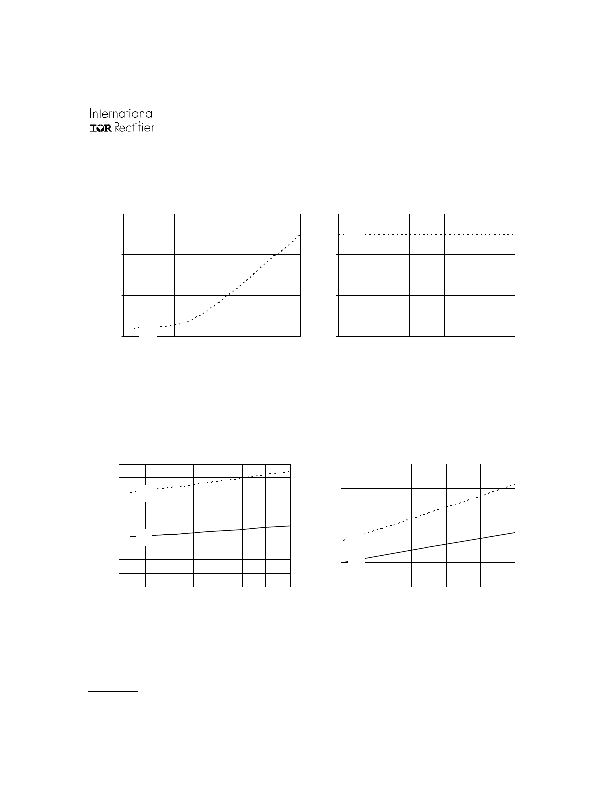
Figure 5A. Turn-On Rise Time vs.
Temperature
Typ
Max
0
10
20
30
40
50
60
10
12
14
16
18
20
Supply Voltage (V)
Figure 5B. Turn-On Rise Time vs. Supply
Voltage
Typ
Max
0
5
10
15
20
25
30
35
40
45
-50
-25
0
25
50
75
100
125
Temperature (°C)
Tu
rn
-O
ff
Fa
ll T
im
e
(
ns
)
Figure 6A. Turn-Off Fall Time vs.
Temperature
Typ
Max
0
10
20
30
40
50
60
10
12
14
16
18
20
Supply Voltage (V)
Figure 6B. Turn-Off Fall Tim e vs. Supply
Voltage
T
u
r
n
-
O
n
R
i
s
e
T
i
m
e
(
n
s
)
Tu
rn
-O
ff
Fa
ll T
im
e
(
ns
)
Not recommended for new designs. No replacement is available
www.irf.com
8
IRS21851SPbF
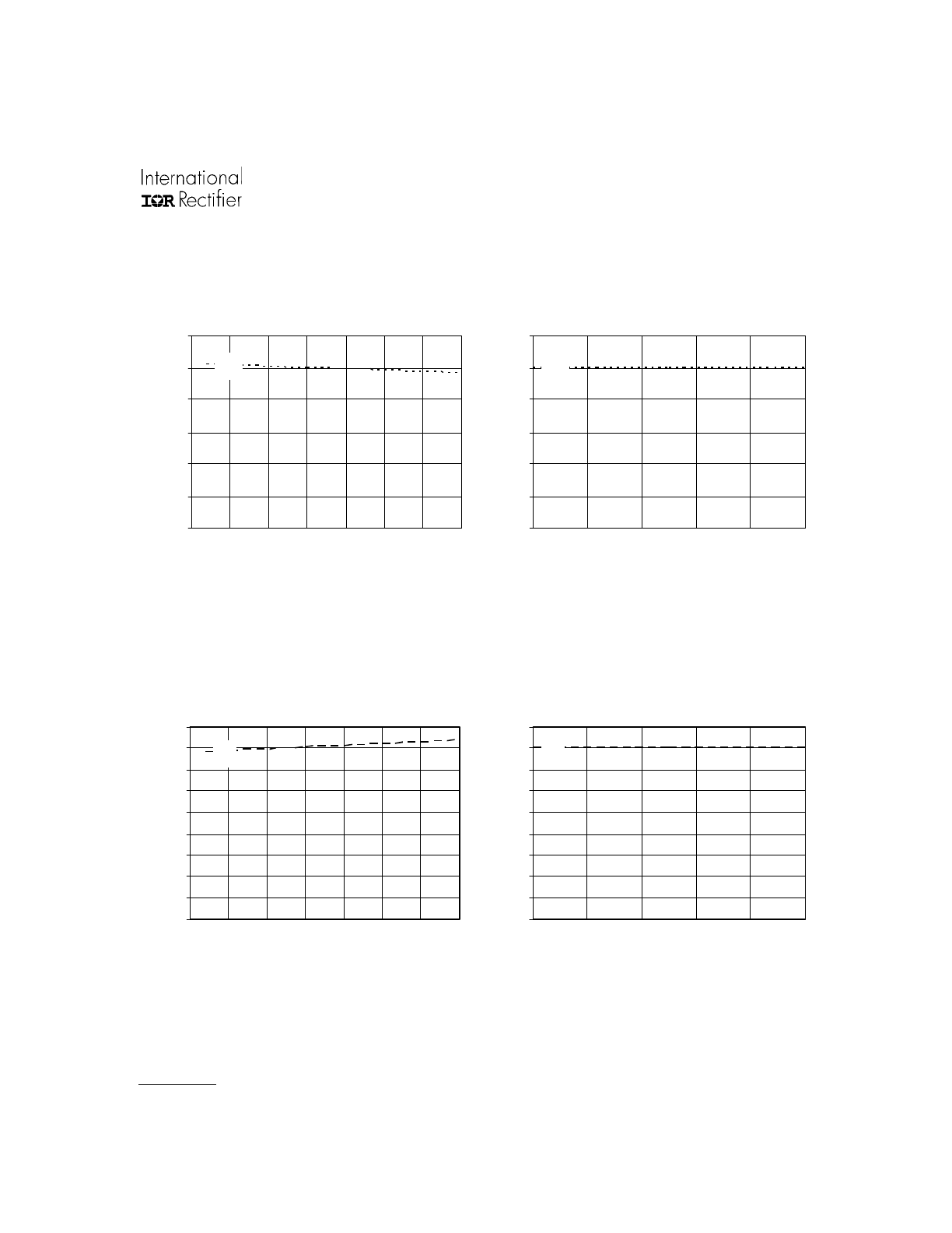
Max
0
0.5
1
1.5
2
2.5
3
-50
-25
0
25
50
75
100
125
Temperature (°C)
Lo
gi
c
"1
" I
np
ut
V
ol
ta
ge
(
V)
Figure 7A. Logic "1" Input Voltage vs.
Temperature
Max
0
0.5
1
1.5
2
2.5
3
10
12
14
16
18
20
Supply Voltage (V)
Lo
gi
c
"1
" I
np
ut
V
ol
ta
ge
(
V)
Figure 7B. Logic "1" Input Voltage vs. Supply
Voltage
Min
0
0.1
0.2
0.3
0.4
0.5
0.6
0.7
0.8
0.9
-50
-25
0
25
50
75
100
125
Temperature (°C)
Lo
gi
c
"0
" I
np
ut
V
ol
ta
ge
(
V)
Figure 8A. Logic "0" Input Voltage vs.
Temperature
Min
0
0.1
0.2
0.3
0.4
0.5
0.6
0.7
0.8
0.9
10
12
14
16
18
20
Supply Voltage (V)
Lo
gi
c
"0
" I
np
ut
V
ol
ta
ge
(
V)
Figure 8B. Logic "0" Input Voltage vs. Supply
Voltage
Not recommended for new designs. No replacement is available
www.irf.com
9
IRS21851SPbF
Typ
Max
0
10
20
30
40
50
60
70
80
90
-50
-25
0
25
50
75
100
125
Temperature (°C)
H
ig
h
Le
ve
l O
ut
pu
t
(m
V)
Figure 9A. High Level Output vs.
Temperature (Io = 2 mA)
Typ
Max
0
10
20
30
40
50
60
70
10
12
14
16
18
20
Supply Voltage (V)
H
i
g
h
L
e
v
e
l O
u
t
p
u
t
(
m
V
)
Figure 9B. High Level Output vs. Supply
Voltage (Io =2 mA)
Typ
Max
0
5
10
15
20
25
30
35
40
-50
-25
0
25
50
75
100
125
Temperature (°C)
Lo
w
L
ev
el
O
ut
pu
t
(m
V)
Figure 10A. Low Level Output vs.
Temperature (Io=2 mA)
Typ
Max
0
5
10
15
20
25
30
35
10
12
14
16
18
20
Supply Voltage (V)
Lo
w
L
ev
el
O
ut
pu
t
(m
V)
Figure 10B. Low Level Output vs. Supply
Voltage (Io=2 mA)
Not recommended for new designs. No replacement is available
www.irf.com
10
IRS21851SPbF
Max
0
50
100
150
200
250
300
-50
-25
0
25
50
75
100
125
Temperature (°C)
O
ffs
et
S
up
pl
y
Le
ak
ag
e
C
ur
re
nt
(µ
A)
Figure 11A. Offset Supply Leakag
e Current
vs. Temperature
Max
0
10
20
30
40
50
60
10
12
14
16
18
20
Supply Voltage (V)
O
f
f
s
e
t S
u
p
p
l
y
L
e
a
k
a
g
e
C
u
r
r
e
n
t (
µ
A
)
Figure 11B. Offse t Supply Leak age Current vs.
Supply Voltage
Typ
Max
0
20
40
60
80
100
120
140
160
180
-50
-25
0
25
50
75
100
125
Temperature (°C)
V
B
S
S
up
pl
y
C
ur
re
nt
(
µA
)
Figure 12A. V
BS
Supply Current vs.
Temperature
Typ
Max
0
50
100
150
200
250
10
12
14
16
18
20
Supply Voltage (V)
V
B
S
S
up
pl
y
C
ur
re
nt
(
µA
)
Figure 12B. V
BS
Supply Curre nt vs. Supply
Voltage
Not recommended for new designs. No replacement is available