
ww.irf.com
© 2008 International Rectifier
July 1, 2009
IRS2123S/IRS2124S
HIGH SIDE DRIVER IC
Features
• Floating channel designed for bootstrap operation
• Fully operational to +600 V
• Tolerant to negative transient voltage – dV/dt immune
• Gate drive supply range from 10 V to 20 V
• Undervoltage
lockout
• CMOS Schmitt-triggered inputs with pull-down
• Output in phase with input (IRS2123) or out of
Phase with input (IRS2124)
• Leadfree, RoHS compliant
Typical Applications
• General purpose single highside inverters
Product Summary
Topology Single
highside
V
OFFSET
≤ 600 V
V
OUT
10 V – 20 V
I
o+
& I
o-
(typical)
500 mA
t
ON
& t
OFF
(typical)
140 ns & 140 ns
Package Options
8-Lead SOIC
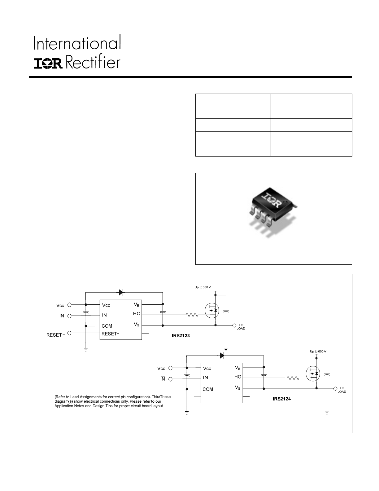
Typical Connection Diagram
Not recommended for new designs. For new designs, we recommend IRS2117SPBF or IRS25752LPBF for IRS2123SPBF and IRS2118SPBF or IRS25752LPBF for IRS2124SPBF
IRS2123S, IRS2124S
www.irf.com
© 2008 International Rectifier
2
Table of Contents
Page
Description
3
Qualification Information
4
Absolute Maximum Ratings
5
Recommended Operating Conditions
5
Static Electrical Characteristics
6
Dynamic Electrical Characteristics
6
Functional Block Diagram
7
Input/Output Pin Equivalent Circuit Diagram
8
Lead Definitions
9
Lead Assignments
9
Application Information and Additional Details
10
Parameter Temperature Trends
11
Package Details
15
Tape and Reel Details
16
Part Marking Information
17
Ordering Information
18
Not recommended for new designs. For new designs, we recommend IRS2117SPBF or IRS25752LPBF for IRS2123SPBF and IRS2118SPBF or IRS25752LPBF for IRS2124SPBF

IRS2123S, IRS2124S
www.irf.com
© 2008 International Rectifier
3
Description
The IRS2123S/IRS2124S are high voltage, high speed power MOSFET and IGBT drivers. Proprietary
HVIC and latch immune CMOS technologies enable ruggedized monolithic construction. The logic input is
compatible with standard CMOS outputs. The output drivers feature a high pulse current buffer stage
designed for minimum cross-conduction. The floating channel can be used to drive an N-channel power
MOSFET or IGBT in the high- side configuration which operates up to 600 V.
Not recommended for new designs. For new designs, we recommend IRS2117SPBF or IRS25752LPBF for IRS2123SPBF and IRS2118SPBF or IRS25752LPBF for IRS2124SPBF
IRS2123S, IRS2124S
www.irf.com
© 2008 International Rectifier
4
Qualification Information
†
Industrial
††
Qualification Level
Comments: This family of ICs has passed JEDEC’s
Industrial qualification. IR’s Consumer qualification level is
granted by extension of the higher Industrial level.
Moisture Sensitivity Level
MSL3
†††
260°C
(per IPC/JEDEC J-STD-020)
Machine Model
Class B
(per JEDEC standard JESD22-A115)
ESD
Human Body Model
Class 2
(per EIA/JEDEC standard EIA/JESD22-A114)
IC Latch-Up Test
Class I, Level A
(per JESD78)
RoHS Compliant
Yes
†
Qualification standards can be found at International Rectifier’s web site
http://www.irf.com/
†† Exceptions to AEC-Q100 requirements are noted in the qualification report.
††† Higher MSL ratings may be available for the specific package types listed here. Please contact your
International Rectifier sales representative for further information.
Not recommended for new designs. For new designs, we recommend IRS2117SPBF or IRS25752LPBF for IRS2123SPBF and IRS2118SPBF or IRS25752LPBF for IRS2124SPBF
IRS2123S, IRS2124S
www.irf.com
© 2008 International Rectifier
5
Absolute Maximum Ratings
Absolute Maximum Ratings indicate sustained limits beyond which damage to the device may occur. All
voltage parameters are absolute voltages referenced to GND, all currents are defined positive into any
lead. This is a stress only rating and operation of the device at these or any conditions exceeding those
indicated in the operational sections of this specification is not implied
Symbol Definition
Min.
Max.
Units
V
BS
High Side Floating Supply Voltage
-0.3 25 V
V
B
High Side Driver Output Stage Voltage
-0.3 625 V
V
S
High Side Floating Supply Offset Voltage
V
B
- 25
V
B
+ 0.3
V
V
H
O
Output Voltage Gate Connection
V
S
– 0.3
V
B
+ 0.3
V
V
CC
Supply
Voltage
-0.3 25 V
V
IN
Input
Voltage
-0.3
V
CC
+ 0.3
V
V
RES
Reset Input Voltage
-0.3
V
CC
+ 0.3
V
dV/dt
Allowable Offset Voltage Slew Rate
-50
50
V/nsec
T
J
Junction
Temperature
-55 150
T
S
Storage
Temperature
-55 150
ºC
Recommended Operating Conditions
For proper operations the device should be used within the recommended conditions.
Symbol Definition
Min.
Max.
Units
V
B
High Side Driver Output Stage Voltage
-10V Transient 0.4 us
V
S
+10 V
S
+20 V
V
S
High Side Floating Supply Offset Voltage
-25V Transient 0.4 µs
†
600 V
V
H
O
Output Voltage Gate Connection
V
S
V
B
V
V
CC
Supply Voltage
10
20
V
V
IN
Input Voltage
0
V
CC
V
V
RES
Reset Input Voltage
0
V
CC
V
T
A
Ambient Temperature (f
s
<60kHz, V
BS
=14V,
C
load
=2,5nF, R=50Ohm)
-40 125 ºC
† Logic operational for V
S
of -5 to +600 V. Logic state held for V
S
of -5 V to – V
BS.
(Please refer to the Design Tip DT97-3 for more details).
Not recommended for new designs. For new designs, we recommend IRS2117SPBF or IRS25752LPBF for IRS2123SPBF and IRS2118SPBF or IRS25752LPBF for IRS2124SPBF
IRS2123S, IRS2124S
www.irf.com
© 2008 International Rectifier
6
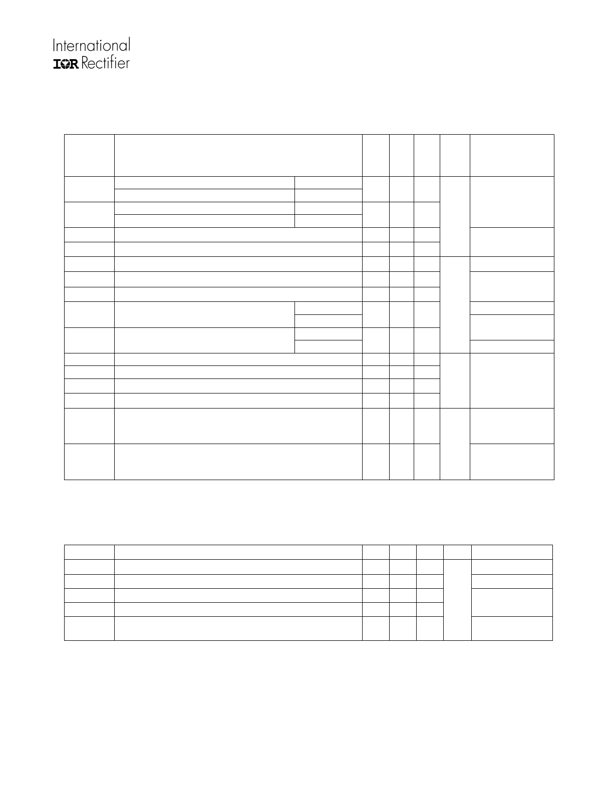
Static Electrical Characteristics
V
BIAS
(V
CC
, V
BS
) = 15 V and T
A
= 25°C unless otherwise specified. The V
IL,
V
IH
and I
IN
parameters are
referenced to COM. The V
O
and I
O
parameters are referenced to COM and are applicable to the
respective output leads: HO and LO.
Dynamic Electrical Characteristics
V
BIAS
(V
CC
, V
BS
) = 15 V, C
L
= 1000 pF, T
A
= 25°C unless otherwise specified. The dynamic electrical
characteristics are measured using the test circuit shown in Fig. 3.
Symbol Definition Min Typ Max
Units
Test
Conditions
Logic “1” input voltage
IRS2123
V
IH
Logic “0” input voltage
IRS2124
0.70
*V
CC
— —
Logic “0” input voltage
IRS2123
V
IL
Logic “1” input voltage
IRS2124
— —
0.35
*V
CC
V
OH
High level output voltage, V
BIAS
-
V
O
—
—
2
V
OL
Low level output voltage, V
O
—
0.1
0.2
V
I
O
= 10 mA
I
LK
Offset supply leakage current
—
—
50
V
B
=
V
S
= 600 V
I
QBS
Quiescent
V
BS
supply current
—
— 240
I
QCC
Quiescent
V
CC
supply current
—
— 500
V
IN
= 0 V or V
CC
IRS2123
V
IN
= V
CC
I
IN+
Logic “1” input bias current
IRS2124
— — 5.0
IRS2123
V
IN
= 0 V
I
IN-
Logic “0” input bias current
IRS2124
— — 5.0
µA
V
IN
= V
CC
V
BSUV+
V
BS
supply undervoltage positive going threshold
7.2 8.6
9.6
V
BSUV-
V
BS
supply undervoltage negative going threshold
6.6 8.0
9.0
V
CCUV+
V
CC
supply undervoltage positive going threshold
7.2 8.6
9.6
V
CCUV-
V
CC
supply undervoltage negative going threshold 6.6 8.0
9.0
V
I
O+
Output high short circuit pulsed current
250 500
—
V
O
= 0 V,
V
IN
= Logic “1”
PW ≤ 10 µs
I
O-
Output low short circuit pulsed current
250 500
—
mA
V
O
= 15 V,
V
IN
= Logic “0”
PW ≤ 10 µs
Symbol Definition
Min
Typ Max
Units
Test
Conditions
t
on
Turn-on propagation delay
— 140 240
V
S
= 0 V
t
off
Turn-off propagation delay
— 140 240
V
S
= 600 V
t
r
Turn-on rise time
—
80 200
t
f
Turn-off fall time
—
80 200
t
RES
RESET to output turn off propagation delay
(IRS2123 only)
— 170 300
ns
Not recommended for new designs. For new designs, we recommend IRS2117SPBF or IRS25752LPBF for IRS2123SPBF and IRS2118SPBF or IRS25752LPBF for IRS2124SPBF
IRS2123S, IRS2124S
www.irf.com
© 2008 International Rectifier
7
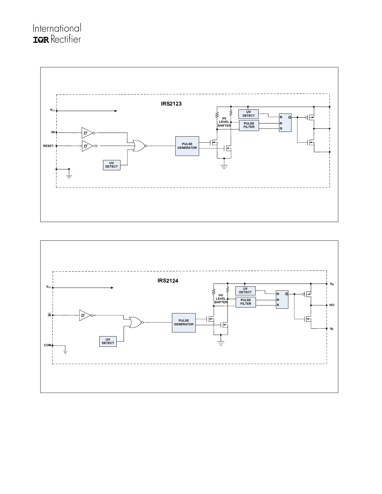
Functional Block Diagram (IRS2123)
Functional Block Diagram (IRS2124)
Not recommended for new designs. For new designs, we recommend IRS2117SPBF or IRS25752LPBF for IRS2123SPBF and IRS2118SPBF or IRS25752LPBF for IRS2124SPBF
IRS2123S, IRS2124S
www.irf.com
© 2008 International Rectifier
8
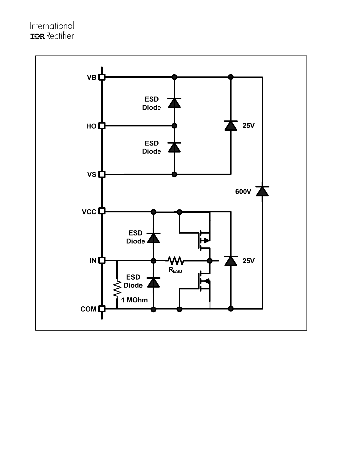
I/O Pin Equivalent Circuit Diagram
Not recommended for new designs. For new designs, we recommend IRS2117SPBF or IRS25752LPBF for IRS2123SPBF and IRS2118SPBF or IRS25752LPBF for IRS2124SPBF
IRS2123S, IRS2124S
www.irf.com
© 2008 International Rectifier
9
Lead Definitions
Pin Symbol
Pin
description
1 VCC
Low side and logic fixed supply
2
IN
IN-
Logic input for gate driver output (HO), in phase with HO (IRS2123)
Logic input for gate driver output (HO), out of phase with HO (IRS2124)
3 COM
Logic
Ground
4
RESET-
NC
Driver Enable Signal Input (negative logic) (IRS2123)
No connection (IRS2124)
5
NC
No connection
6 V
S
High-side floating supply return
7 H
O
High-side gate drive output
8 V
B
High-side floating supply
IRS2123S
IRS2124S
IN-
RESET-
NC
NC
NC
Not recommended for new designs. For new designs, we recommend IRS2117SPBF or IRS25752LPBF for IRS2123SPBF and IRS2118SPBF or IRS25752LPBF for IRS2124SPBF
IRS2123S, IRS2124S
www.irf.com
© 2008 International Rectifier
10
Application Information and Additional Details
IRS2123 logic table for Vcc, VBS, RESET, IN, and H
O
Vcc
VBS
RESET-
IN
H
O
X X X
LOW
OFF
X X LOW X OFF
<VccUVLO-
X X X OFF
X <VBSUVLO- X
X
OFF
>VccUVLO+ >VBSUVLO+ HIGH
HIGH
ON
RESET = HIGH indicates that high side NMOS is allowed to be turned on.
RESET = LOW indicates that high side NMOS is OFF.
IN = HIGH indicates that high side NMOS is on.
IN = LOW indicates that high side NMOS is off.
X = independent
IRS2124 logic table for Vcc, VBS, RESET, IN, and H
O
Vcc
VBS IN-
H
O
X X
HIGH
OFF
<VccUVLO- X
X OFF
X <VBSUVLO- X
OFF
>VccUVLO+ >VBSUVLO+ LOW
ON
IN- = HIGH indicates that high side NMOS is on.
IN- = LOW indicates that high side NMOS is off.
X = independent
Not recommended for new designs. For new designs, we recommend IRS2117SPBF or IRS25752LPBF for IRS2123SPBF and IRS2118SPBF or IRS25752LPBF for IRS2124SPBF