
June 12, 2008
IRS210614S
HIGH AND LOW SIDE DRIVER
IC Features
• Floating channel designed for bootstrap
operation
• Fully operational to +600 V
• Tolerant to negative transient voltage, dV/dt
immune
• Gate drive supply range from 10 V to 20 V
• Undervoltage lockout for both channels
• 3.3 V, 5 V, and 15 V input logic compatible
• Matched propagation delay for both channels
• Logic and power ground +/- 5 V offset
• Lower di/dt gate driver for better noise
immunity
• Outputs in phase with inputs
• RoHS
compliant
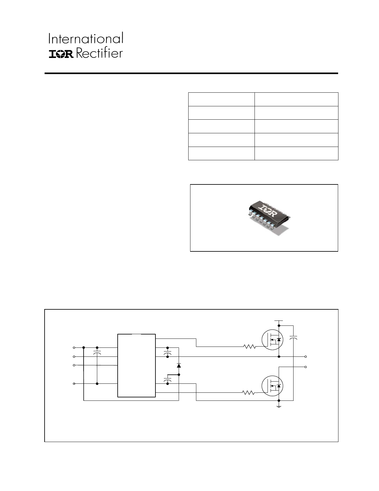
Typical Connection Diagram
Product Summary
Topology Half-Bridge
V
OFFSET
600 V
V
OUT
10 V-20 V
I
O+
& I
O-
(typical)
290 mA & 600 mA
Ton & toff (typical)
165 ns & 165 ns
Package Types
SO14N
www.irf.com
© 2008 International Rectifier
1
up to 600 V
TO
LOAD
V
CC
V
B
V
S
HO
LO
COM
HIN
V
SS
LIN
V
CC
V
SS
LIN
HIN
Note: Please refer to page 10 for the correct pin configuration. This diagram shows electrical connections only.
Please refer to our Application Notes and Design Tips for proper circuit board layout.
Not recommended for new designs. For new designs, we recommend IRS21064SPBF or 2EDL05N06PJ
IRS210614S
www.irf.com
© 2008 International Rectifier
2
PRELIMINARY
Table of Contents
Page
Description
3
Qualification Information
4
Absolute Maximum Ratings
5
Recommended Operating Conditions
6
Static Electrical Characteristics
7
Dynamic Electrical Characteristics
7
Functional Block Diagram
8
Input/Output Pin Equivalent Circuit Diagram
9
Lead Definitions
10
Lead Assignments
10
Waveform Definitions
11
Package Details
12
Tape and Reel Details
13
Part Marking Information
14
Ordering Information
15
Not recommended for new designs. For new designs, we recommend IRS21064SPBF or 2EDL05N06PJ

IRS210614S
www.irf.com
© 2008 International Rectifier
3
PRELIMINARY
Description
The IRS21064S is a high voltage, high speed power MOSFET and IGBT driver with independent high and
low-side referenced output channels. Proprietary HVIC and latch immune CMOS technologies enable
ruggedized monolithic construction. The logic input is compatible with standard CMOS or LSTTL output,
down to 3.3 V logic. The output drivers feature a high pulse current buffer stage designed for minimum
driver cross-conduction. The floating channel can be used to drive an N-channel power MOSFET or IGBT
in the high side configuration which operates up to 600 V.
Not recommended for new designs. For new designs, we recommend IRS21064SPBF or 2EDL05N06PJ
IRS210614S
www.irf.com
© 2008 International Rectifier
4
PRELIMINARY
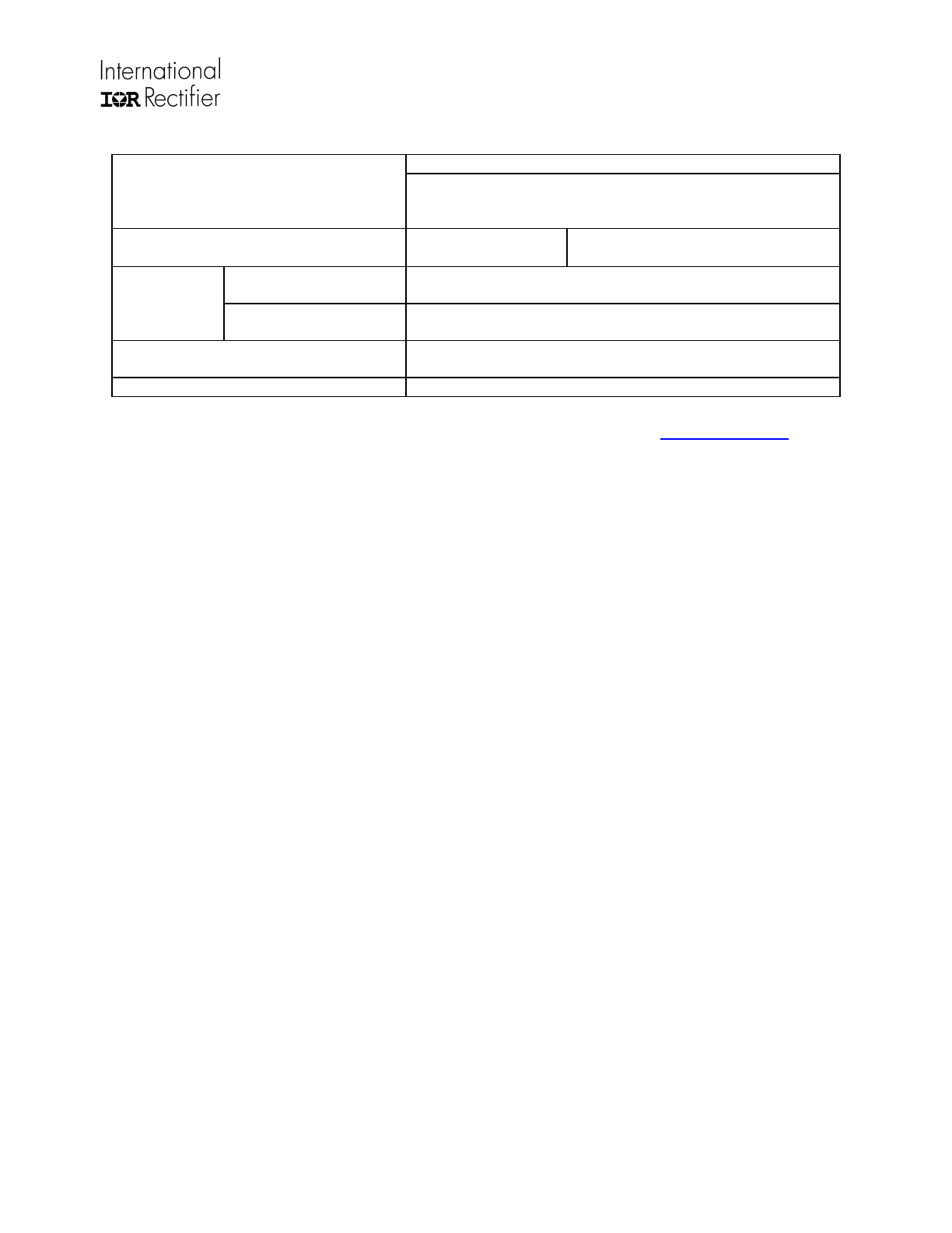
Qualification Information
†
Industrial
††
Qualification Level
Comments: This family of ICs has passed JEDEC’s
Industrial qualification. IR’s Consumer qualification level is
granted by extension of the higher Industrial level.
Moisture Sensitivity Level
SOIC14N
MSL2
†††
(per IPC/JEDEC J-STD-020)
Machine Model
Class B
(per JEDEC standard EIA/JESD22-A115)
ESD
Human Body Model
Class 2
(per EIA/JEDEC standard JESD22-A114)
IC Latch-Up Test
Class 1, Level A
(per JESD78)
RoHS Compliant
Yes
†
Qualification standards can be found at International Rectifier’s web site
http://www.irf.com/
††
Higher qualification ratings may be available should the user have such requirements. Please
contact your International Rectifier sales representative for further information.
††† Higher MSL ratings may be available for the specific package types listed here. Please contact
your International Rectifier sales representative for further information.
Not recommended for new designs. For new designs, we recommend IRS21064SPBF or 2EDL05N06PJ
IRS210614S
www.irf.com
© 2008 International Rectifier
5
PRELIMINARY
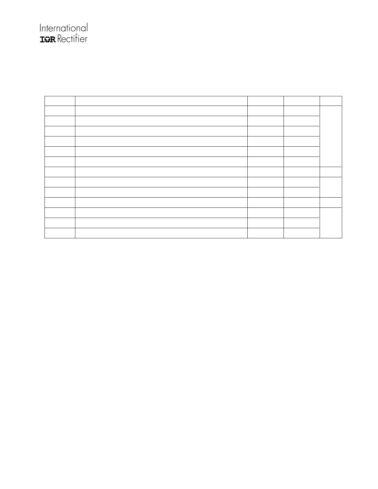
Absolute Maximum Ratings
Absolute maximum ratings indicate sustained limits beyond which damage to the device may occur. All
voltage parameters are absolute voltages referenced to COM, all currents are defined positive into any
lead. The thermal resistance and power dissipation ratings are measured under board mounted and still air
conditions.
Symbol Definition
Min.
Max.
Units
VB
High-side floating supply absolute voltage
-0.3
625
VS
High-side floating supply offset voltage
VB - 25
VB + 0.3
VHO
High-side floating output voltage
VS - 0.3
VB + 0.3
VCC
Low-side output voltage
-0.3
25
VLO Low-side and logic fixed supply voltage
-0.3
VCC + 0.3
VIN
Logic input voltage
VS -0.3
VCC + 0.3
V
VSS
Logic ground
VCC -25
VCC + 0.3
V/ns
dV
S
/dt
Allowable offset supply voltage transient
---
50
PD
Package power dissipation @ TA ≤ +25 ºC
--- 1.0
W
RthJA Thermal resistance, junction to ambient
---
120
ºC/W
TJ
Junction temperature
---
150
TS
Storage temperature
-50
150
TL
Lead temperature (soldering, 10 seconds)
---
300
ºC
Not recommended for new designs. For new designs, we recommend IRS21064SPBF or 2EDL05N06PJ
IRS210614S
www.irf.com
© 2008 International Rectifier
6
PRELIMINARY
Recommended Operating Conditions
The input/output logic timing diagram is shown in Fig. 1. For proper operation the device should be used
within the recommended conditions. The V
S
and V
SS
offset rating are tested with all supplies biased at a
15 V differential..
Symbol Definition
Min.
Max.
Units
VB
High-side floating supply absolute voltage
VS + 10
VS + 20
VS
High-side floating supply offset voltage
Note 1
600
VHO
High-side floating output voltage
VS
VB
VCC
Low-side output voltage
10
VLO
Low-side and logic fixed supply voltage
0
VCC
VIN
Logic input voltage
VSS
VCC
VSS
Logic ground
-5
5
V
TA
Ambient temperature
-40
125
ºC
Logic operational for VS of -5 V to +600 V. Logic state held for VS of -5 V to -VBS.
(Please refer to the Design Tip DT97-3 for more details).
†
Not recommended for new designs. For new designs, we recommend IRS21064SPBF or 2EDL05N06PJ
IRS210614S
www.irf.com
© 2008 International Rectifier
7
PRELIMINARY
Static Electrical Characteristics
V
BIAS
(V
CC
, V
BS
) = 14 V, C
T
= 1 nF and T
A
= 25 °C unless otherwise specified. The V
O
and I
O
parameters
are referenced to COM and are applicable to the respective output leads: HO or LO.
CLO1=CLO2=CHO1=CHO2=1 nF.
Symbol Definition Min
Typ
Max
Units
Test Conditions
Low Voltage Supply Characteristics
VIH
Logic “1” input voltage
2.5
—
—
VIL
Logic “0” input voltage
—
—
0.8
V
VCC = 10 V to 20V
VOH
High level output voltage, V
BIAS
-V
O
—
0.05
0.2
VOL
Low level output voltage, V
O
—
0.02
0.1
Io = 2 mA
ILK
Offset supply leakage current
—
—
50
VB = VS = 600 V
IQBS
Quiescent VBS supply current
20 75 130
IQCC
Quiescent VCC supply current
60 120 180
VIN = 0 V or 5V
IIN+
Logic “1” input bias current VIN = 5 V
—
5 20
IIN-
Logic “0” input bias current VIN = 0 V
—
—
5
µA
VCCUV+
VBSUV
VCC and VBS supply undervoltage
positive going threshold
8.0 8.9 9.8
VCCUV-
VBSUV-
VCC and VBS supply undervoltage
negative going threshold
7.4 8.2 9.0
VCCUVH
VBSUVH
Hysteresis 0.3
0.7
—
V
Io+
Output high short circuit pulsed current
130
290
—
VO = 0 V,
PW
≤ 10 µs
Io-
Output low short circuit pulsed current
270
600
—
mA
VO = 15 V,
PW
≤ 10 µs
Dynamic Electrical Characteristics
V
BIAS
(V
CC
, V
BS
) = 15 V, V
SS
= COM, C
L
= 1000 pF, T
A
= 25 °C.
Symbol
Component
Min.
Typ.
Max. Units
Test Conditions
ton
Turn-on propagation delay
---
165
230
V
S
= 0 V
toff
Turn-off propagation delay
---
165
230
V
S
= 0 V or 600 V
MT
Delay matching, HS & LS turn-on/off
---
0
30
tr
Turn-on rise time
---
100
220
tf
Turn-off fall time
---
35
80
ns
V
S
= 0 V
Not recommended for new designs. For new designs, we recommend IRS21064SPBF or 2EDL05N06PJ
IRS210614S
www.irf.com
© 2008 International Rectifier
8
PRELIMINARY
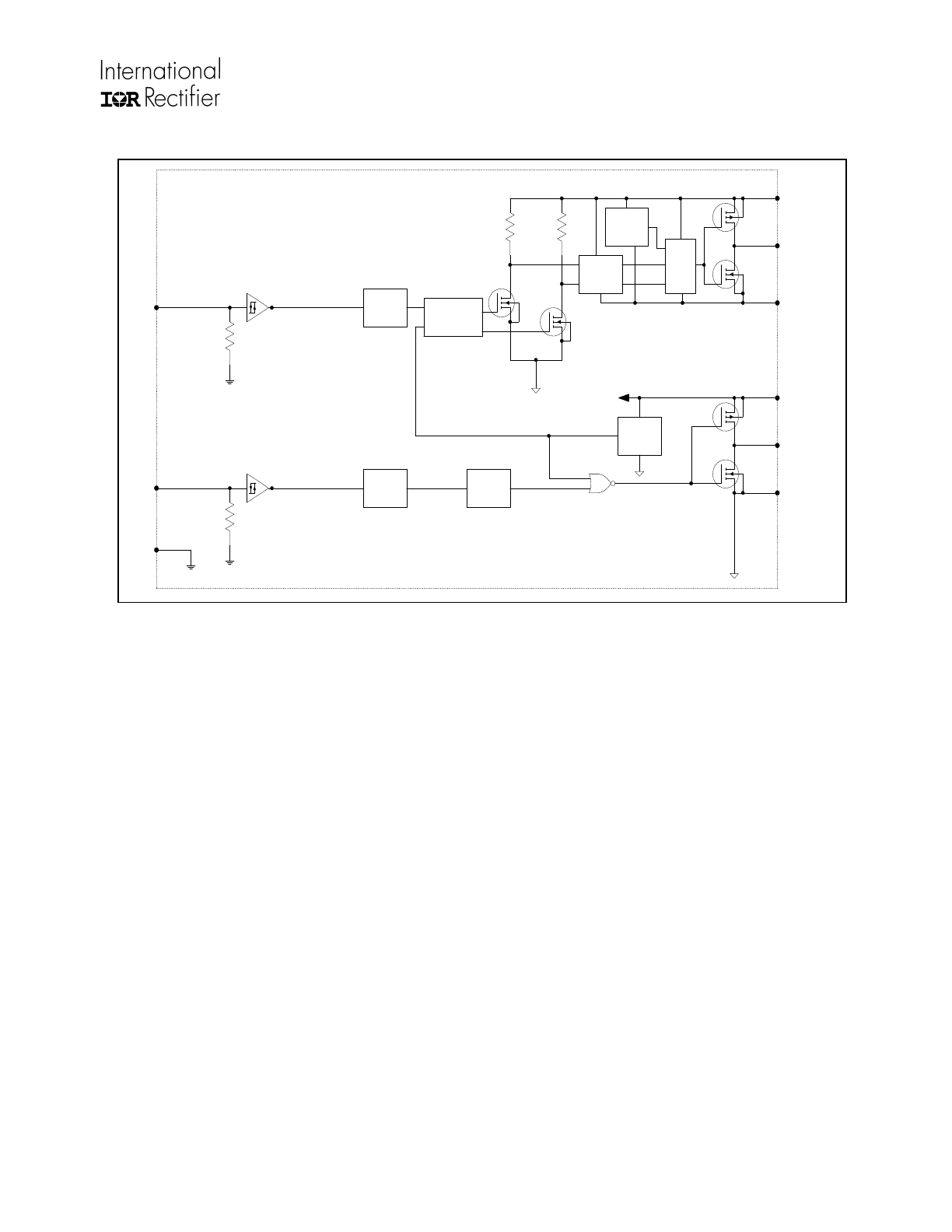
Functional Block Diagram
IRS21064
LIN
UV
DETECT
DELAY
COM
LO
VCC
HIN
VSS
VS
HO
VB
PULSE
FILTER
HV
LEVEL
SHIFTER
R
R
S
Q
UV
DETECT
PULSE
GENERATOR
VSS/COM
LEVEL
SHIFT
VSS/COM
LEVEL
SHIFT
IRS210614
Not recommended for new designs. For new designs, we recommend IRS21064SPBF or 2EDL05N06PJ
IRS210614S
www.irf.com
© 2008 International Rectifier
9
PRELIMINARY
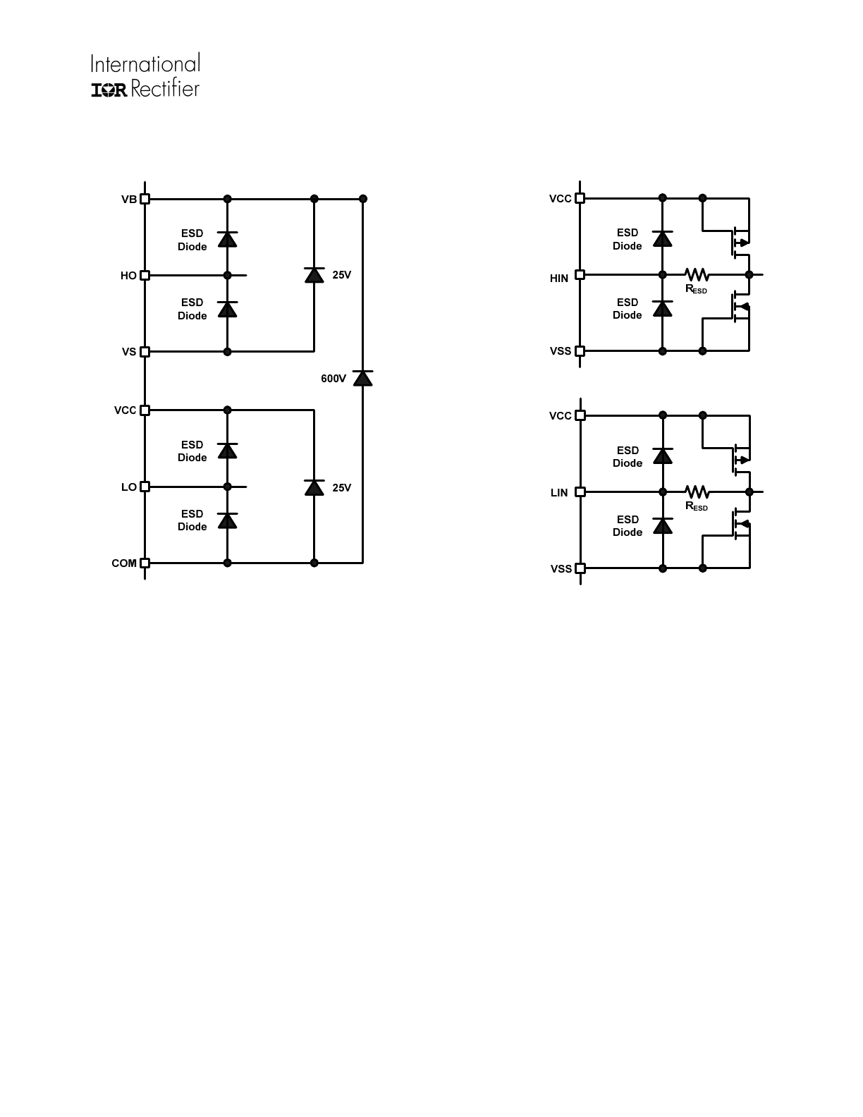
I/O Pin Equivalent Circuit Diagrams
Not recommended for new designs. For new designs, we recommend IRS21064SPBF or 2EDL05N06PJ
IRS210614S
www.irf.com
© 2008 International Rectifier
10
PRELIMINARY
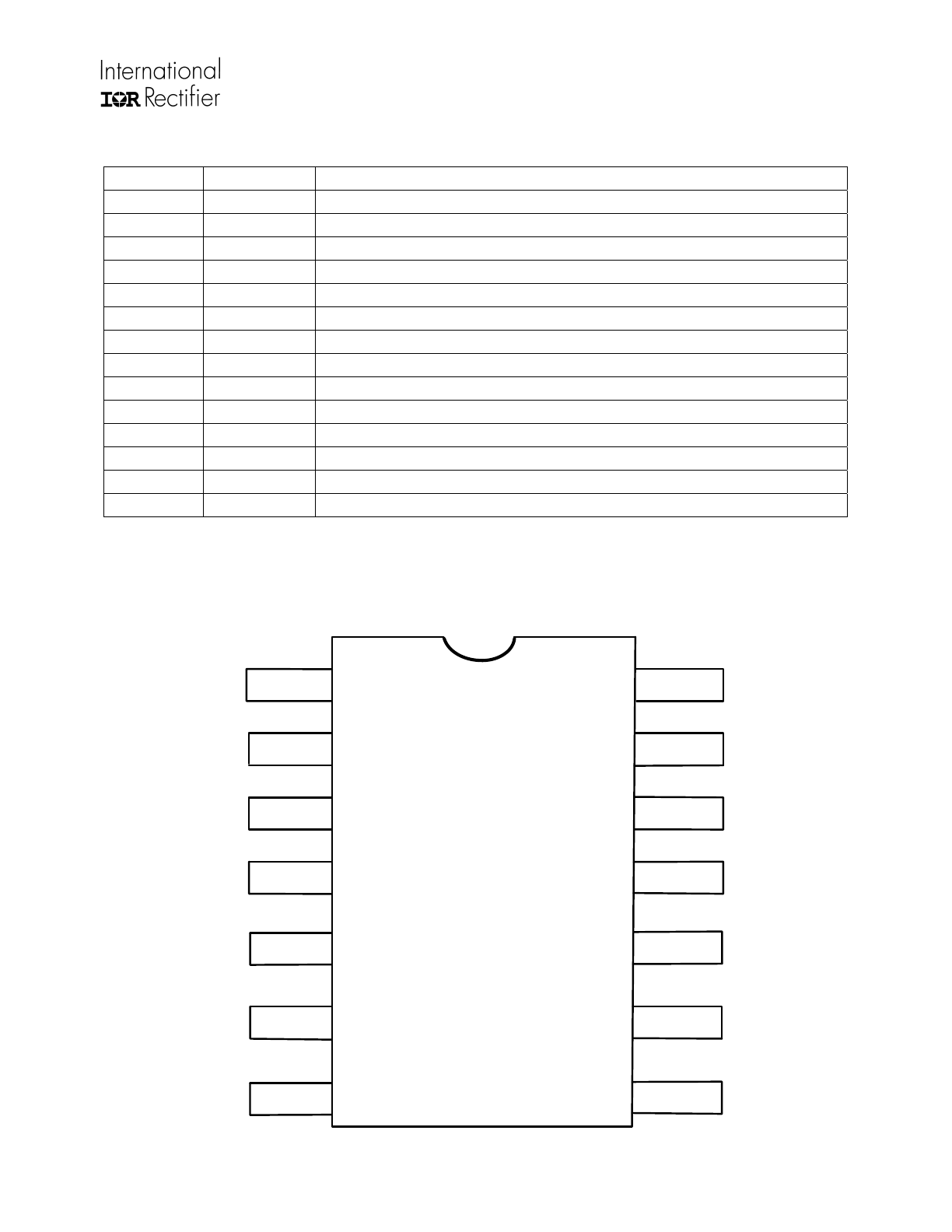
Lead Definitions
Pin#
Symbol
Description
1 V
CC
Low-side and logic fixed supply
2
HIN
Logic input for high-side gate driver output (HO), in phase
3
LIN
Logic input for low-side gate driver output (LO), in phase
4 NC
No
Connect
5 V
SS
Logic
ground
6 COM
Low-side
return
7
LO
Low-side drive output
8 NC
No
Connect
9 NC
No
Connect
10 NC
No
Connect
11 V
S
High-side floating supply return
12
HO
High-side gate drive output
13 V
B
High-side floating supply
14 NC
No
Connect
Lead Assignments
14
13
12
V
B
1
V
S
HO
COM
4
5
7
6
2
3
LO
V
SS
11
10
9
8
NC
NC
NC
NC
NC
V
CC
HIN
LIN
Not recommended for new designs. For new designs, we recommend IRS21064SPBF or 2EDL05N06PJ