

IRMCK171
1
www.irf.com
© 2014 International Rectifier
Submit Datasheet Feedback
May 28, 2014
High Performance Sensorless Motor Control IC
Description
IRMCK171 is a high performance One Time Programmable ROM based motion control IC designed and
optimized for appliance control which contains two computation engines integrated into one monolithic
chip. One is the Flexible Motion Control Engine (MCE
TM
) for sensorless control of permanent magnet
motors or induction motors; the other is an 8-bit high-speed microcontroller (8051). The user can program
a motion control algorithm by connecting these control elements using a graphic compiler. Key
components of the complex sensorless control algorithms, such as the Angle Estimator, are provided as
complete pre-defined control blocks. A unique analog/digital circuit and algorithm fully supports single
shunt or leg shunt current reconstruction. IRMCK171 comes in a 48 pin QFP package.
Features
• MCE
TM
(Flexible Motion Control Engine) -
Dedicated computation engine for high
efficiency sinusoidal sensorless motor control
• Built-in hardware peripheral for single or two
shunt current feedback reconstruction and
analog circuits
• Supports induction machine and both interior
and surface permanent magnet motor
sensorless control
• Loss minimization Space Vector PWM
• Two-channel analog output (PWM)
• Embedded 8-bit high speed microcontroller
(8051) for flexible I/O and man-machine control
• JTAG programming port for
emulation/debugger
• Serial communication interface (UART)
• I2C/SPI serial interface
• Internal 32Kbyte OTP ROM
• 3.3V single supply
Product Summary
Maximum clock input (fcrystal) 60
MHz
Maximum Internal clock (SYSCLK)
128MHz
Maximum 8051 clock (8051CLK)
32MHz
MCE
TM
computation data range 16 bit
signed
8051/MCE Data RAM
2KB
MCE Program RAM 12KB
PWM carrier frequency 20 bits/ SYSCLK
A/D input channels
7
A/D converter resolution 12 bits
A/D converter conversion speed
2 μsec
Analog output (PWM) resolution 8 bits
UART baud rate (typ)
57.6 Kbps
Number of digital I/O (max)
10
Package (lead free) QFP48
Maximum 3.3V operating current 60mA
Base Part Number
Package Type
Standard Pack
Orderable Part Number
Form
Quantity
IRMCK171
QFP
Tray
2500
IRMCK171TY
Tape and Reel
2000
IRMCK171TR

IRMCK171
2
www.irf.com
© 2014 International Rectifier
Submit Datasheet Feedback
May 28, 2014
Table of Contents
1
Overview ............................................................................................................................... 5
2
Pinout .................................................................................................................................... 6
3
IRMCK171 Block Diagram and Main Functions .................................................................... 7
4
Application connection and Pin function ............................................................................... 9
4.1
8051 Peripheral Interface Group ................................................................................. 10
4.2
Motion Peripheral Interface Group .............................................................................. 11
4.3
Analog Interface Group ............................................................................................... 11
4.4
Power Interface Group ................................................................................................ 11
4.5
Test Interface Group ................................................................................................... 11
5
DC Characteristics .............................................................................................................. 13
5.1
Absolute Maximum Ratings ......................................................................................... 13
5.2
System Clock Frequency and Power Consumption .................................................... 13
5.3
Digital I/O DC Characteristics ...................................................................................... 14
5.4
Analog I/O (IFB+,IFB-,IFBO, AIN5+,AIN5-,AIN5O) DC Characteristics ...................... 15
5.5
Under Voltage Lockout DC characteristics.................................................................. 16
5.6
Itrip comparator DC characteristics ............................................................................. 16
5.7
CMEXT and AREF Characteristics ............................................................................. 16
6
AC Characteristics .............................................................................................................. 17
6.1
Digital PLL AC Characteristics .................................................................................... 17
6.2
Analog to Digital Converter AC Characteristics ........................................................... 18
6.3
Op amp AC Characteristics ......................................................................................... 19
6.4
SYNC to SVPWM and A/D Conversion AC Timing ..................................................... 20
6.5
GATEKILL to SVPWM AC Timing ............................................................................... 21
6.6
Itrip AC Timing ............................................................................................................. 21
6.7
Interrupt AC Timing ..................................................................................................... 22
6.8
I
2
C AC Timing .............................................................................................................. 22
6.9
SPI AC Timing ............................................................................................................. 23
6.10
UART AC Timing ......................................................................................................... 25
6.11
CAPTURE Input AC Timing ........................................................................................ 26
6.12
OTP Programming Timing ........................................................................................... 27
6.13
JTAG AC Timing ......................................................................................................... 28
7
I/O Structure ........................................................................................................................ 29
8
Pin List ................................................................................................................................ 32
9
Package Dimensions .......................................................................................................... 34
10 Part Marking Information ..................................................................................................... 35
11 Qualification Information ..................................................................................................... 35

IRMCK171
3
www.irf.com
© 2014 International Rectifier
Submit Datasheet Feedback
May 28, 2014
List of Tables
Table 1 Absolute Maximum Ratings ........................................................................................... 13
Table 2 System Clock Frequency ............................................................................................... 13
Table 3 Digital I/O DC Characteristics ........................................................................................ 14
Table 5 Analog I/O DC Characteristics ....................................................................................... 15
Table 6 UVcc DC Characteristics ............................................................................................... 16
Table 7 Itrip DC Characteristics .................................................................................................. 16
Table 8 CMEXT and AREF DC Characteristics .......................................................................... 16
Table 9 PLL AC Characteristics .................................................................................................. 17
Table 10 A/D Converter AC Characteristics ............................................................................... 18
Table 11 Current Sensing OP Amp AC Characteristics .............................................................. 19
Table 12 SYNC AC Characteristics ............................................................................................ 20
Table 13 GATEKILL to SVPWM AC Timing................................................................................ 21
Table 14 Itrip AC Timing ............................................................................................................. 21
Table 15 Interrupt AC Timing ...................................................................................................... 22
Table 16 I
2
C AC Timing .............................................................................................................. 22
Table 17 SPI Write AC Timing .................................................................................................... 23
Table 18 SPI Read AC Timing .................................................................................................... 24
Table 19 UART AC Timing ......................................................................................................... 25
Table 20 CAPTURE AC Timing .................................................................................................. 26
Table 21 OTP Programming Timing ........................................................................................... 27
Table 22 JTAG AC Timing .......................................................................................................... 28
Table 23 Pin List ......................................................................................................................... 33

IRMCK171
4
www.irf.com
© 2014 International Rectifier
Submit Datasheet Feedback
May 28, 2014
List of Figures
Figure 1 Typical Application Block Diagram Using IRMCK171 ........................................................................ 5
Figure 2 Pinout of IRMCK171 ........................................................................................................................... 6
Figure 3 Crystal circuit example ...................................................................................................................... 17
Figure 4 Voltage droop and S/H hold time ...................................................................................................... 18
Figure 5 A capacitor of 47pF is recommended at the output pin of all op amps. ........................................... 19
Figure 6 SYNC timing ..................................................................................................................................... 20
Figure 7 Gatekill timing ................................................................................................................................... 21
Figure 8 ITRIP timing ...................................................................................................................................... 21
Figure 9 Interrupt timing .................................................................................................................................. 22
Figure 10 I
2
C Timing ....................................................................................................................................... 22
Figure 11 SPI write timing ............................................................................................................................... 23
Figure 12 SPI read timing ............................................................................................................................... 24
Figure 13 UART timing.................................................................................................................................... 25
Figure 14 CAPTURE timing ............................................................................................................................ 26
Figure 15 OTP programming timing ................................................................................................................ 27
Figure 16 JTAG timing .................................................................................................................................... 28
Figure 17 PWMUL/PWMUH/PWMVL/PWMVH/PWMWL/PWMWH output .................................................... 29
Figure 18 All digital I/O except motor PWM output ......................................................................................... 29
Figure 19 RESET, GATEKILL I/O ................................................................................................................... 30
Figure 20 Analog input .................................................................................................................................... 30
Figure 21 Analog operational amplifier output and AREF I/O structure ....................................................... 30
Figure 22 VPP programming pin I/O structure ................................................................................................ 31
Figure 23 VSS and AVSS pin structure .......................................................................................................... 31
Figure 24 VDD1 and VDDCAP pin structure .................................................................................................. 31
Figure 25 XTAL0/XTAL1 pins structure .......................................................................................................... 31
IRMCK171
5
www.irf.com
© 2014 International Rectifier
Submit Datasheet Feedback
May 28, 2014
1 Overview
IRMCK171 is a new generation International Rectifier integrated circuit device primarily designed as a
one-chip solution for complete inverter controlled appliance motor control applications. Unlike a traditional
microcontroller or DSP, the IRMCK171 provides a built-in closed loop sensorless control algorithm using
the unique flexible Motion Control Engine (MCE
TM
) for permanent magnet motors as well as induction
motors. The MCE
TM
consists of a collection of control elements, motion peripherals, a dedicated motion
control sequencer and dual port RAM to map internal signal nodes. IRMCK171 also employs a unique
single shunt current reconstruction circuit in addition to two leg shunt current sensing circuit to eliminate
additional analog/digital circuitry and enables a direct shunt resistor interface to the IC. Motion control
programming is achieved using a dedicated graphical compiler integrated into the MATLAB/Simulink
TM
development environment. Sequencing, user interface, host communication, and upper layer control
tasks can be implemented in the 8051 high-speed 8-bit microcontroller. The 8051 microcontroller is
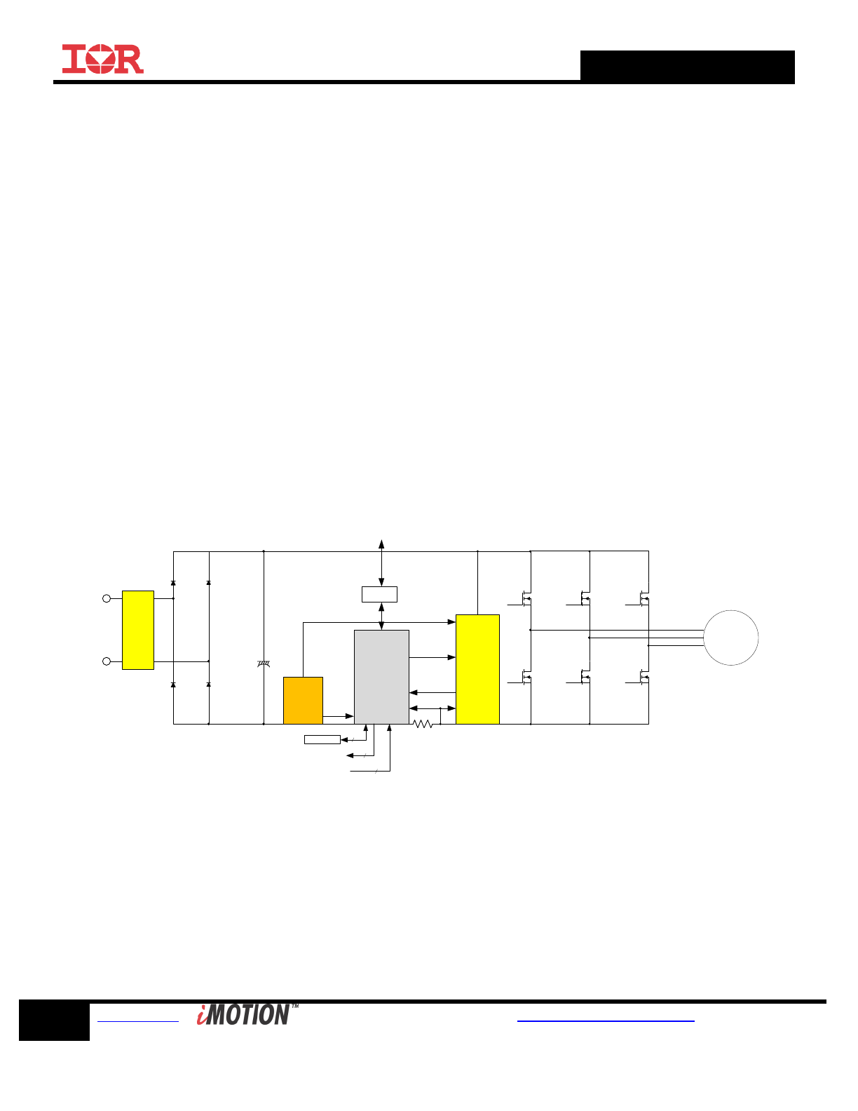
equipped with a JTAG port to facilitate emulation and debugging tools. Figure 1 shows a typical
application schematic using the IRMCK171.
IRMCK171 contains 32K bytes of OTP program ROM, The IRMCF171 contains 64K bytes of Flash RAM
and intended for development purposes only while the IRMCK171 is intended for volume production.
Both the development and ROM versions come in a 48-pin QFP package with identical pin configuration
to facilitate PC board layout and transition to mass production.
IRMCK171
Power
Supply
IRS2336D
PM motor
IPM or SPM
Or
IM motor
Passive
EMI
Fillter
Digital I/O
Analog Input
Host
Communication
(RS232C)
Appliance PM
motor Drive
3.3V
Gate signal
15V
EEPROM
6
2
8
Galvanic
isolation
Optional
Figure 1 Typical Application Block Diagram Using IRMCK171
IRMCK171
6
www.irf.com
© 2014 International Rectifier
Submit Datasheet Feedback
May 28, 2014
2 Pinout
Pin out shown is based on QFP48 pin package.
17 18 19 20 21 22 23 24
25
26
27
28
29
30
31
32
15
14
16
3
12
4
11
5
6
7
8
9
10
2
1
XTAL0
XTAL1
P
1
.1
/RXD
P
1
.2
/TXD
VDD1
VSS
VDDCAP
P1.3/SYNC/SCK
P1.4/CAP
P3.2/INT0
34
35
36
33
46
37
45
38
44 43 42 41 40 39
47
48
VSS
VDDCAP
AVSS
AREF
P
2
.7
/AOPWM
1
PWMUH
PWMVH
PWMWH
PWMUL
PWMVL
PWMWL
GATEKILL
IFB
O
IFB
+
IFB
-
RESET
VPP
/P
1
.5
TCK
TDI
/P
5
.1
TDO
/P
5
.3
TMS
/P
5
.2
SDA/CS0
SCL/SO-SI
IRMCK171
(Top View)
AIN
2
CMEXT
P2.0/NMI
P1.0/T2
P
3
.0
/CS
1
13
AIN
3
AIN
4
VDD1
AIN
1
AIN
0
AIN5+
AIN
5
-
AIN5O
P
3
.3
/INT
1
P3.1/AOPWM2
Figure 2 Pinout of IRMCK171
IRMCK171
7
www.irf.com
© 2014 International Rectifier
Submit Datasheet Feedback
May 28, 2014
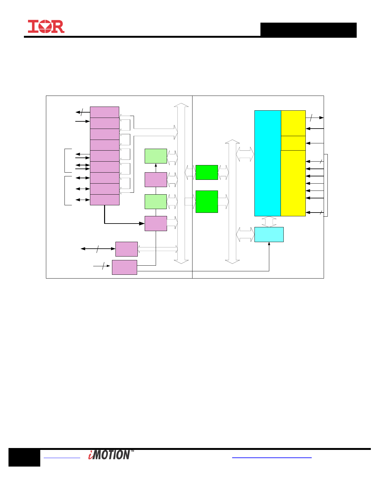
3 IRMCK171 Block Diagram and Main Functions
IRMCK171 block diagram is shown in Figure 3.
Motion Control
Sequencer
Dual Port
RAM
2kbyte
MCE
Program
RAM
12kbyte
Program
ROM/RAM
32kB
8
bit uP Address
/data bus
Motion Control Bus
A/D
MUX
S/H
D/A
(PWM)
Timer
Counnter0,1,2
Watchdog
Timer
Motion
Control
Modules
UART
I2C
SND
RCV
6
Low Loss
SVPWM
AIN0
GATEKILL
To IGBT
gate drive
Mini-Motion
Control
Engine
(MiniMCE)
Monitoring
Host
Interface
Digital
I/Os
8bit (8051)
microcontroller
AIN1
AIN2
JTAG
Emulator
Debugger
4
Freq
Synthesizer
2
Ceramic
Resonator
(4MHz)
32MHz
AIN3
analog
input
2
Capture
Interrupt
Control
Single Shunt
Motor Current
Reconstruction
From
shunt
resistor
Speed
command
PORT 1
SCL
SDA
PORT 2
PORT 3
AIN4
8bit
CPU
Core
Local
RAM
2kbyte
128MHz
IFB
3
AIN5
3
Figure 3 IRMCK171 Block Diagram
IRMCK171 contains the following functions for sensorless AC motor control applications:
• Motion Control Engine (MCE
TM
)
o
Sensorless FOC (complete sensorless field oriented control)
o
Proportional plus Integral block
o
Low pass filter
o
Differentiator and lag (high pass filter)
o
Ramp
o
Limit
o
Angle estimate (sensorless control)
o
Inverse Clark transformation
o
Vector rotator
o
Bit latch
o
Peak detect

IRMCK171
8
www.irf.com
© 2014 International Rectifier
Submit Datasheet Feedback
May 28, 2014
o
Transition
o
Multiply-divide (signed and unsigned)
o
Divide (signed and unsigned)
o
Adder
o
Subtractor
o
Comparator
o
Counter
o
Accumulator
o
Switch
o
Shift
o
ATAN (arc tangent)
o
Function block (any curve fitting, nonlinear function)
o
16 bit wide Logic operations (AND, OR, XOR, NOT, NEGATE)
o
MCE
TM
program memory and dual port RAM (max 12K+2k byte)
o
MCE
TM
control sequencer
• 8051 microcontroller
o
Two 16 bit timer/counters
o
One 16 bit periodic timer
o
One 16 bit watchdog timer
o
One 16 bit capture timer
o
Up to 24 discrete I/Os
o
Six-channel 12 bit A/D
Buffered (current sensing) one channel (0 – 1.2V input)
Unbuffered seven channels (0 – 1.2V input)
o
JTAG port (4 pins)
o
Up to three channels of analog output (8 bit PWM)
o
UART
o
I
2
C/SPI port
o
32K byte OTP program ROM
o
2K byte data RAM
IRMCK171
9
www.irf.com
© 2014 International Rectifier
Submit Datasheet Feedback
May 28, 2014
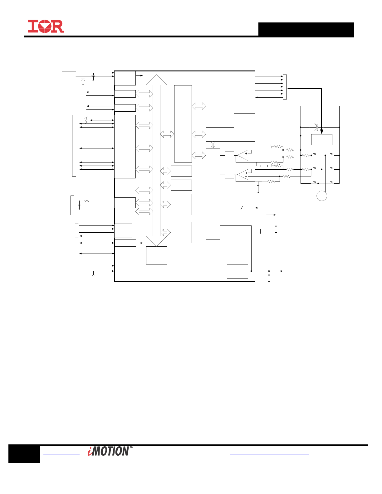
4 Application connection and Pin function
P1.2/TXD
P1.1/RXD
P1.3/SYNC/SCK
XTAL0
PWMUH
PWMUL
PWMVH
PWMVL
PWMWH
PWMWL
GATEKILL
AIN0,AIN1,AIN2, AIN3
Host
Microcontroller
(RS232C)
Digital I/O
Control
System
Clock
4MHz
Crystal
Analog Output
XTAL1
P1.4/CAP
P3.0/CS1
RESET
P5.1/TDI
JTAG Control
(OTP programming
& Emulation)
TCLK
P5.2/TMS
TDO
AVREF
IFBC+
IFBC-
IFBCO
Other analog input (0-1.2V)
AVDD
1.8V
AVSS
VDD1
3.3V
VSS
CMEXT
AIN5+
AIN5-
AIN5O
Optional External Voltage
Reference (0.6V)
P2.7/AOPWM1
SCL/SO-SI
SDA/CS0
Other Communication
(I
2
C)
Frequency
Synthesizer
RS232C
I
2
C/SPI
PORT1
PORT2
RESET
PWM1
JTAG
Interface
Low Loss
Space
Vector
PWM
S/H
S/H
8051
CPU
Dual
Port
Memory
(2kB)
&
MCE
Memory
(12kB)
Motion
Control
Modules
Motion
Control
Sequencer
12bit
A/D
&
MUX
System
clock
Local
RAM
(2kByte)
Program
RAM
(32kByte)
System
Reset
Watchdog
Timer
Timers
IRMCK171
AREF
PORT3
P1.0/T2
P1.5/VPP
P2.0/NMI
P3.2/INT0
4
3.3V
1.8V
Voltage
Regulator
VDDCAP
3.3V
P3.3/INT1
OTP
Programming
Voltage
(6.5V)
Motor
HVIC
Gate Drive
IRS2336D
AVREF
Single
Shunt
Current
Sensing
Figure 4 IRMCK171 Connection Diagram

IRMCK171
10
www.irf.com
© 2014 International Rectifier
Submit Datasheet Feedback
May 28, 2014
4.1 8051 Peripheral Interface Group
UART Interface
P1.2/TXD
Output, Transmit data from IRMCK171
P1.1/RXD
Input, Receive data to IRMCK171
Discrete I/O Interface
P1.0/T2
Input/output port 1.0, can be configured as Timer/Counter 2 input
P1.1/RXD
Input/output port 1.1, can be configured as RXD input
P1.2/TXD
Input/output port 1.2, can be configured as TXD output
P1.3/SYNC/SCK
Input/output port 1.3, can be configured as SYNC output or SPI clock output,
needs to be pulled up to VDD1 in order to boot from I
2
C EEPROM
P1.4/CAP
Input/output port 1.4, can be configured as Capture Timer input
P1.5/VPP
Input/output port 1.5, or OTP programming voltage
P2.0/NMI
Input/output port 2.0, can be configured as non-maskable interrupt input
P3.2/INT0
Input/output port 3.2, can be configured as INT0 input
P2.7/AOPWM1
Input/output port 2.7, can be configured as AOPWM1 output
P3.0/INT2/CS1
Input/output port 3.0, can be configured as INT2 input or SPI chip select 1
P3.1/AOPWM2
Input/output port 3.1, can be configured as AOPWM2 output
P3.3/INT1
Input/output port 3.3, can be configured as INT1 input
P5.1/TDI
Input port 5.1, configured as JTAG port by default
P5.2/TMS
Input port 5.2, configured as JTAG port by default
Analog Output Interface
P2.7/AOPWM1
Input/output, can be configured as 8-bit PWM output 1 with programmable
carrier frequency
P3.1/AOPWM2
Input/output, can be configured as 8-bit PWM output 2 with programmable
carrier frequency
Crystal Interface
XTAL0
Input, connected to crystal
XTAL1
Output, connected to crystal
Reset Interface
RESET
Input and Output, system reset, doesn’t require external RC time constant
I
2
C Interface
SCL/SO-SI
Output, I
2
C clock output, or SPI data
SDA/CS0
Input/output, I
2
C Data line or SPI chip select 0
I
2
C/SPI Interface
SCL/SO-SI
Output, I
2
C clock output, or SPI data
SDA/CS0
Input/output, I
2
C data line or SPI chip select 0
P1.3/SYNC/SCK
Input/output port 1.3, can be configured as SYNC output or SPI clock output,
needs to be pulled up to VDD1 in order to boot from I
2
C EEPROM
P3.0/INT2/CS1
Input/output port 3.0, can be configured as INT2 input or SPI chip select 1