
Parameter
Typ.
Max.
Units
R
θJA
Maximum Junction-to-Ambient
75
100
°C/W
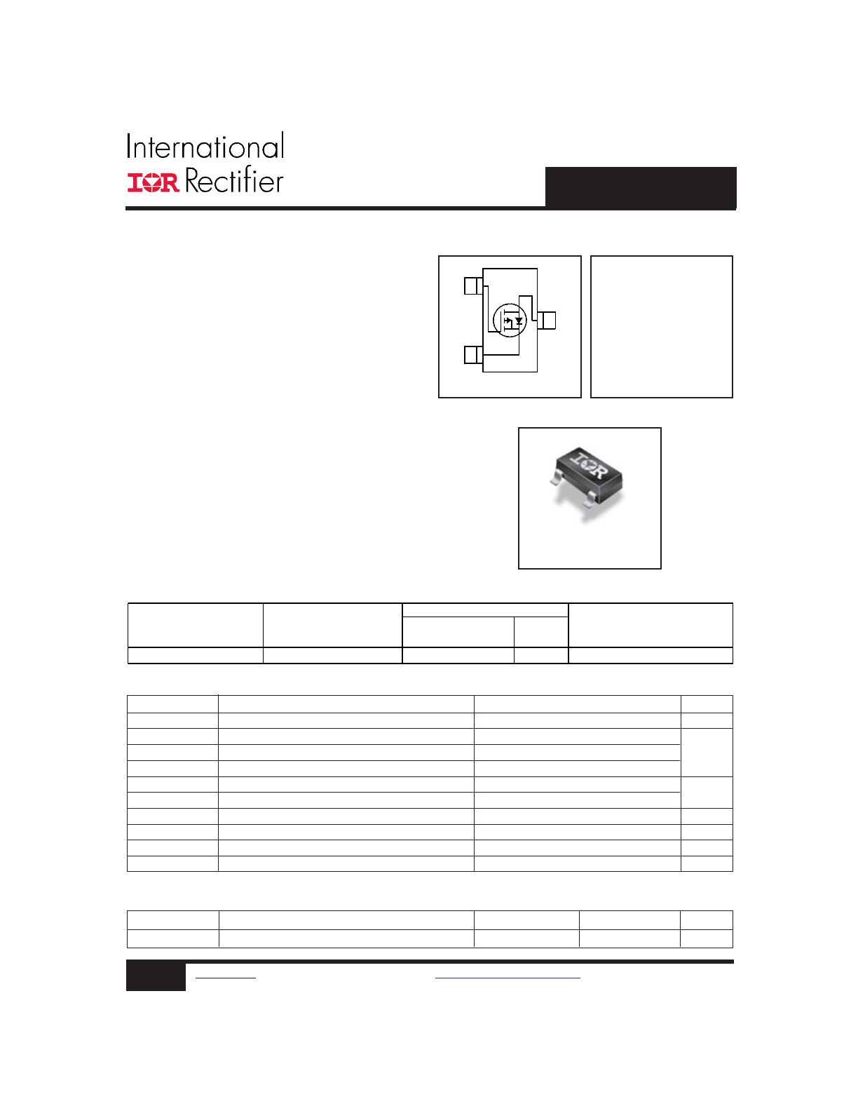
HEXFET
®
Power MOSFET
These P-Channel MOSFETs from International Rectifier utilize advanced
processing techniques to achieve extremely low on-resistance per silicon
area. This benefit, combined with the fast switching speed and ruggedized
device design that HEXFET
®
power MOSFETs are well known for, provides
the designer with an extremely efficient and reliable device for use in battery
and load management.
A thermally enhanced large pad leadframe has been incorporated into the
standard SOT-23 package to produce a HEXFET Power MOSFET with the
industry's smallest footprint. This package, dubbed the Micro3
™, is ideal
for applications where printed circuit board space is at a premium. The low
profile (<1.1mm) of the Micro3 allows it to fit easily into extremely thin
application environments such as portable electronics and PCMCIA
cards. The thermal resistance and power dissipation are the best available.
Thermal Resistance
V
DSS
= -20V
R
DS(on)
= 0.065
Ω
l
Ultra Low On-Resistance
l
P-Channel MOSFET
l
SOT-23 Footprint
l
Low Profile (<1.1mm)
l
Available in Tape and Reel
l
Fast Switching
l
Lead-Free
l
RoHS Compliant, Halogen-Free
Description
Parameter
Max.
Units
V
DS
Drain- Source Voltage
-20
V
I
D
@ T
A
= 25°C
Continuous Drain Current, V
GS
@ -4.5V
-3.7
I
D
@ T
A
= 70°C
Continuous Drain Current, V
GS
@ -4.5V
-2.2
A
I
DM
Pulsed Drain Current
-22
P
D
@T
A
= 25°C
Power Dissipation
1.3
P
D
@T
A
= 70°C
Power Dissipation
0.8
Linear Derating Factor
0.01
W/°C
E
AS
Single Pulse Avalanche Energy
11
mJ
V
GS
Gate-to-Source Voltage
± 12
V
T
J,
T
STG
Junction and Storage Temperature Range
-55 to + 150
°C
Absolute Maximum Ratings
W
Micro3
™
S
G 1
2
D
3
IRLML6402PbF
Form
Quantity
IRLML6402TRPbF
Micro3™ (SOT-23)
Tape and Reel
3000
IRLML6402TRPbF
Package Type
Standard Pack
Orderable Part Number
Base Part Number
1
www.irf.com
©
2014 International Rectifier
Submit Datasheet Feedback
April 28, 2014
2
www.irf.com
©
2014 International Rectifier
Submit Datasheet Feedback
April 28, 2014
IRLML6402PbF
Parameter
Min. Typ. Max. Units
Conditions
I
S
Continuous Source Current
MOSFET symbol
(Body Diode)
––– –––
showing the
I
SM
Pulsed Source Current
integral reverse
(Body Diode)
––– –––
p-n junction diode.
V
SD
Diode Forward Voltage
––– ––– -1.2
V
T
J
= 25°C, I
S
= -1.0A, V
GS
= 0V
t
rr
Reverse Recovery Time
–––
29
43
ns
T
J
= 25°C, I
F
= -1.0A
Q
rr
Reverse RecoveryCharge
–––
11
17
nC
di/dt = -100A/μs
Repetitive rating; pulse width limited by
max. junction temperature.
Notes:
Pulse width ≤ 400μs; duty cycle ≤ 2%.
Source-Drain Ratings and Characteristics
-1.3
-22
A
S
D
G
** For recommended footprint and soldering techniques refer to application note #AN-994.
Surface mounted on 1" square single layer 1oz. copper FR4 board,
steady state.
Starting T
J
= 25°C, L = 1.65mH
R
G
= 25
Ω, I
AS
= -3.7A.
Parameter
Min. Typ. Max. Units
Conditions
V
(BR)DSS
Drain-to-Source Breakdown Voltage
-20
––– –––
V
V
GS
= 0V, I
D
= -250μA
ΔV
(BR)DSS
/
ΔT
J
Breakdown Voltage Temp. Coefficient
––– -0.009 –––
V/°C Reference to 25°C, I
D
= -1mA
––– 0.050 0.065
V
GS
= -4.5V, I
D
= -3.7A
––– 0.080 0.135
V
GS
= -2.5V, I
D
= -3.1A
V
GS(th)
Gate Threshold Voltage
-0.40 -0.55 -1.2
V
V
DS
= V
GS
, I
D
= -250μA
g
fs
Forward Transconductance
6.0
––– –––
S
V
DS
= -10V, I
D
= -3.7A
–––
––– -1.0
V
DS
= -20V, V
GS
= 0V
–––
–––
-25
V
DS
= -20V, V
GS
= 0V, T
J
= 70°C
Gate-to-Source Forward Leakage
–––
––– -100
V
GS
= -12V
Gate-to-Source Reverse Leakage
–––
––– 100
V
GS
= 12V
Q
g
Total Gate Charge
–––
8.0
12
I
D
= -3.7A
Q
gs
Gate-to-Source Charge
–––
1.2
1.8
nC
V
DS
= -10V
Q
gd
Gate-to-Drain ("Miller") Charge
–––
2.8
4.2
V
GS
= -5.0V
t
d(on)
Turn-On Delay Time
–––
350 –––
V
DD
= -10V
t
r
Rise Time
–––
48
–––
I
D
= -3.7A
t
d(off)
Turn-Off Delay Time
–––
588 –––
R
G
= 89
Ω
t
f
Fall Time
–––
381 –––
R
D
= 2.7
Ω
C
iss
Input Capacitance
–––
633 –––
V
GS
= 0V
C
oss
Output Capacitance
–––
145 –––
pF
V
DS
= -10V
C
rss
Reverse Transfer Capacitance
–––
110 –––
ƒ = 1.0MHz
Electrical Characteristics @ T
J
= 25°C (unless otherwise specified)
I
GSS
µA
Ω
R
DS(on)
Static Drain-to-Source On-Resistance
I
DSS
Drain-to-Source Leakage Current
nA
ns
3
www.irf.com
©
2014 International Rectifier
Submit Datasheet Feedback
April 28, 2014
IRLML6402PbF
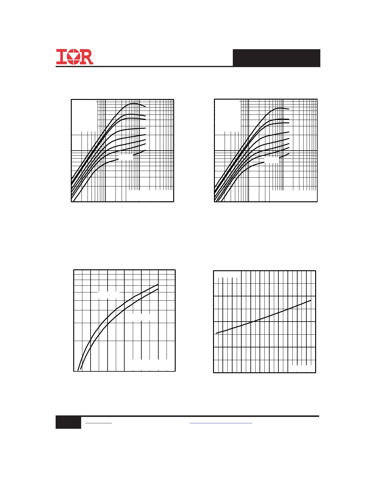
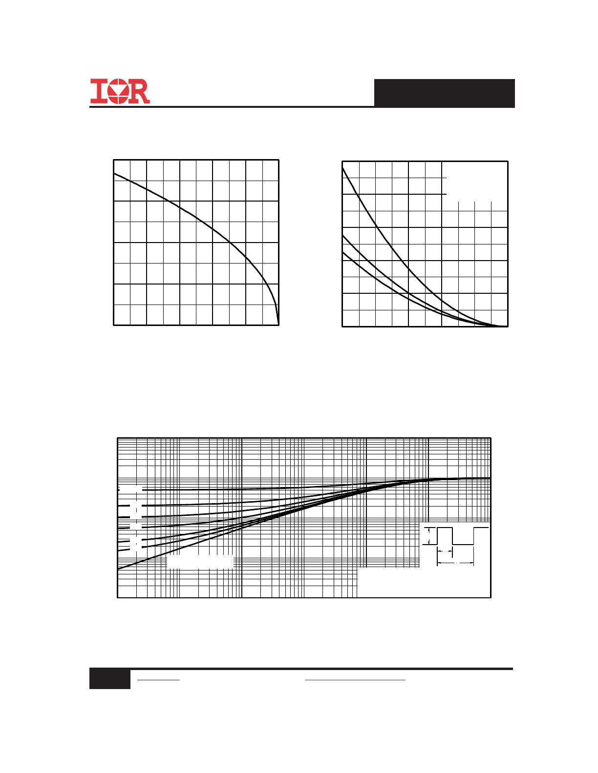
Fig 4. Normalized On-Resistance
Vs. Temperature
Fig 2. Typical Output Characteristics
Fig 1. Typical Output Characteristics
Fig 3. Typical Transfer Characteristics
1
10
100
0.1
1
10
100
20μs PULSE WIDTH
T = 25 C
J
°
TOP
BOTTOM
VGS
-7.00V
-5.00V
-4.50V
-3.50V
-3.00V
-2.70V
-2.50V
-2.25V
-V , Drain-to-Source Voltage (V)
-I , Drain-to-Source Current (A)
DS
D
-2.25V
1
10
100
0.1
1
10
100
20μs PULSE WIDTH
T = 150 C
J
°
TOP
BOTTOM
VGS
-7.00V
-5.00V
-4.50V
-3.50V
-3.00V
-2.70V
-2.50V
-2.25V
-V , Drain-to-Source Voltage (V)
-I , Drain-to-Source Current (A)
DS
D
-2.25V
10
100
2.0
3.0
4.0
5.0
6.0
7.0
8.0
V = -15V
20μs PULSE WIDTH
DS
-V , Gate-to-Source Voltage (V)
-I , Drain-to-Source Current (A)
GS
D
T = 25 C
J
°
T = 150 C
J
°
-60 -40 -20 0
20 40 60 80 100 120 140 160
0.0
0.5
1.0
1.5
2.0
T , Junction Temperature ( C)
R , Drain-to-Source On Resistance
(Normalized)
J
D
S
(on)
°
V
=
I =
GS
D
-4.5V
-3.7A
4
www.irf.com
©
2014 International Rectifier
Submit Datasheet Feedback
April 28, 2014
IRLML6402PbF
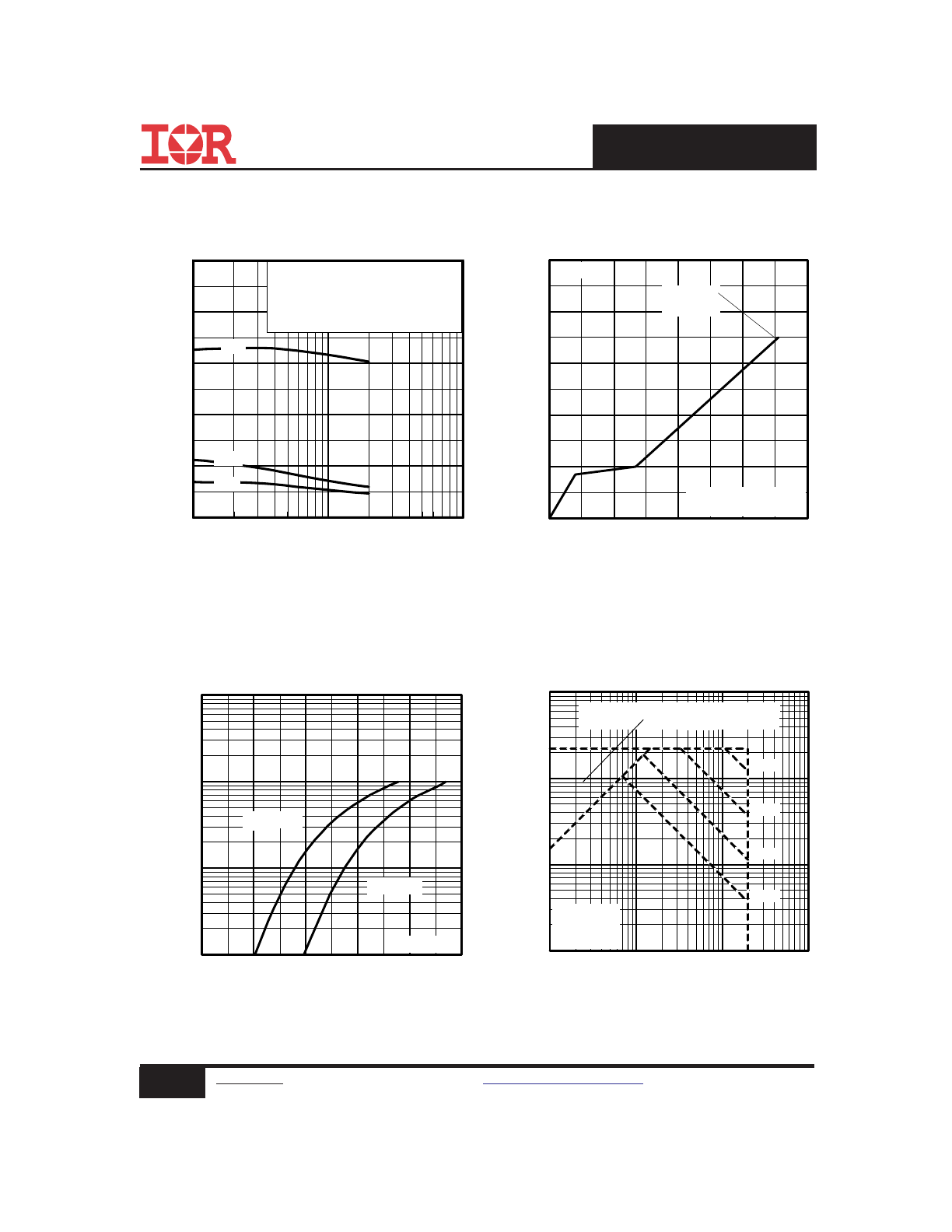
Fig 8. Maximum Safe Operating Area
Fig 6. Typical Gate Charge Vs.
Gate-to-Source Voltage
Fig 5. Typical Capacitance Vs.
Drain-to-Source Voltage
Fig 7. Typical Source-Drain Diode
Forward Voltage
0.1
1
10
100
0.1
1
10
100
OPERATION IN THIS AREA LIMITED
BY R
DS(on)
Single Pulse
T
T
= 150 C
= 25 C
°
°
J
C
-V , Drain-to-Source Voltage (V)
-I , Drain Current (A)I , Drain Current (A)
DS
D
10us
100us
1ms
10ms
1
10
100
VDS, Drain-to-Source Voltage (V)
0
200
400
600
800
1000
C
, C
ap
ac
ita
nc
e(
pF
)
Coss
Crss
Ciss
VGS = 0V, f = 1 MHZ
Ciss = Cgs + Cgd, Cds SHORTED
Crss = Cgd
Coss = Cds + Cgd
0
3
6
9
12
0
2
4
6
8
10
Q , Total Gate Charge (nC)
-V , Gate-to-Source Voltage (V)
G
GS
FOR TEST CIRCUIT
SEE FIGURE
I =
D
13
-3.7A
V
=-10V
DS
0.1
1
10
100
0.2
0.4
0.6
0.8
1.0
1.2
-V ,Source-to-Drain Voltage (V)
-I , Reverse Drain Current (A)
SD
SD
V = 0 V
GS
T = 25 C
J
°
T = 150 C
J
°
5
www.irf.com
©
2014 International Rectifier
Submit Datasheet Feedback
April 28, 2014
IRLML6402PbF
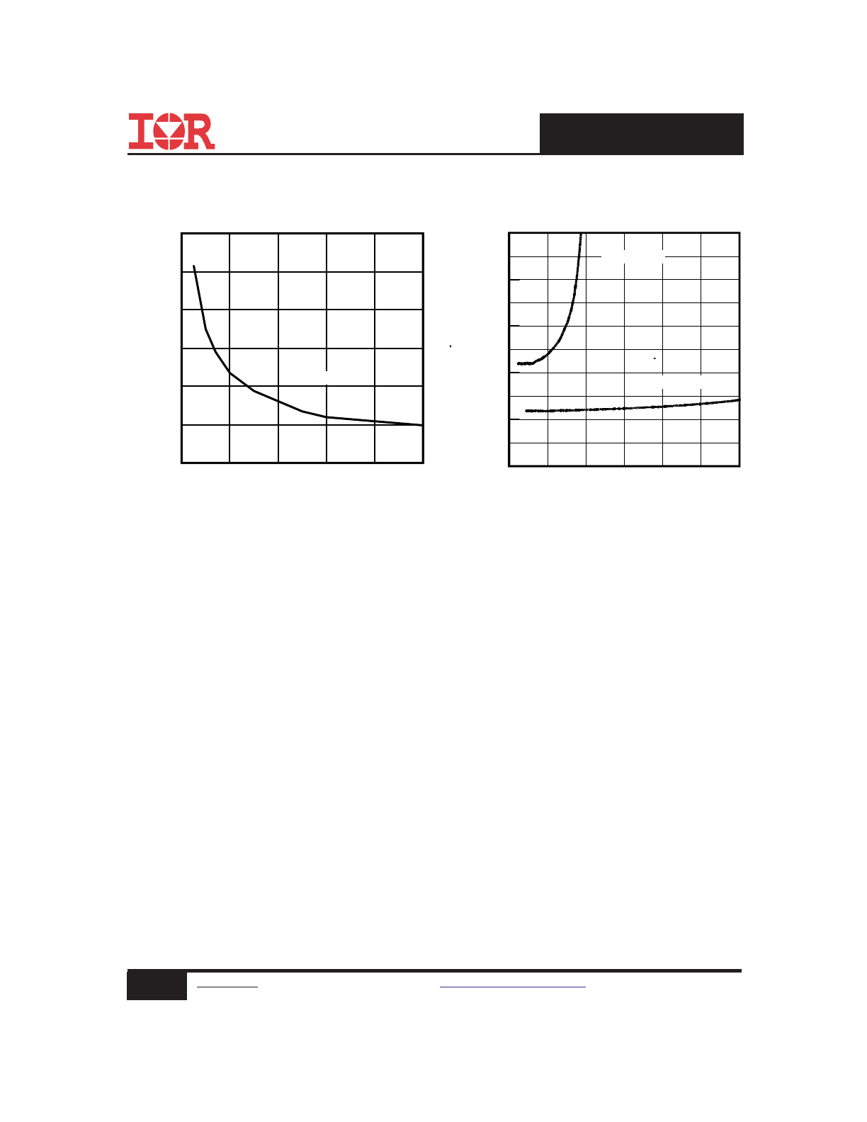
Fig 11. Maximum Effective Transient Thermal Impedance, Junction-to-Ambient
Fig 9. Maximum Drain Current Vs.
Case Temperature
Fig 10. Maximum Avalanche Energy
Vs. Drain Current
25
50
75
100
125
150
0.0
1.0
2.0
3.0
4.0
T , Case Temperature ( C)
-I , Drain Current (A)
°
C
D
25
50
75
100
125
150
0
5
10
15
20
25
Starting T , Junction Temperature ( C)
E , Single Pulse Avalanche Energy (mJ)
J
AS
°
ID
TOP
BOTTOM
-1.7A
-3.0A
-3.7A
0.1
1
10
100
1000
0.00001
0.0001
0.001
0.01
0.1
1
10
Notes:
1. Duty factor D = t / t
2. Peak T = P
x Z
+ T
1
2
J
DM
thJA
A
P
t
t
DM
1
2
t , Rectangular Pulse Duration (sec)
Therm
al
R
esponse
(Z
)
1
th
JA
0.01
0.02
0.05
0.10
0.20
D = 0.50
SINGLE PULSE
(THERMAL RESPONSE)
6
www.irf.com
©
2014 International Rectifier
Submit Datasheet Feedback
April 28, 2014
IRLML6402PbF
Fig 13. Typical On-Resistance Vs.
Drain Current
Fig 12. Typical On-Resistance Vs.
Gate Voltage
2.0
3.0
4.0
5.0
6.0
7.0
-VGS, Gate -to -Source Voltage ( V )
0.02
0.04
0.06
0.08
0.10
0.12
0.14
R
D
S
(o
n)
,
D
ra
in
-t
o
-S
ou
rc
e
V
ol
ta
ge
(
Ω
)
Id = -3.7A
0
5
10
15
20
25
30
-ID , Drain Current ( A )
0.00
0.04
0.08
0.12
0.16
0.20
R
D
S
(
o
n
)
, D
ra
in
-t
o-
S
ou
rc
e
O
n
R
es
is
ta
nc
e
( Ω
)
VGS = -4.5V
VGS = -2.5V
7
www.irf.com
©
2014 International Rectifier
Submit Datasheet Feedback
April 28, 2014
IRLML6402PbF
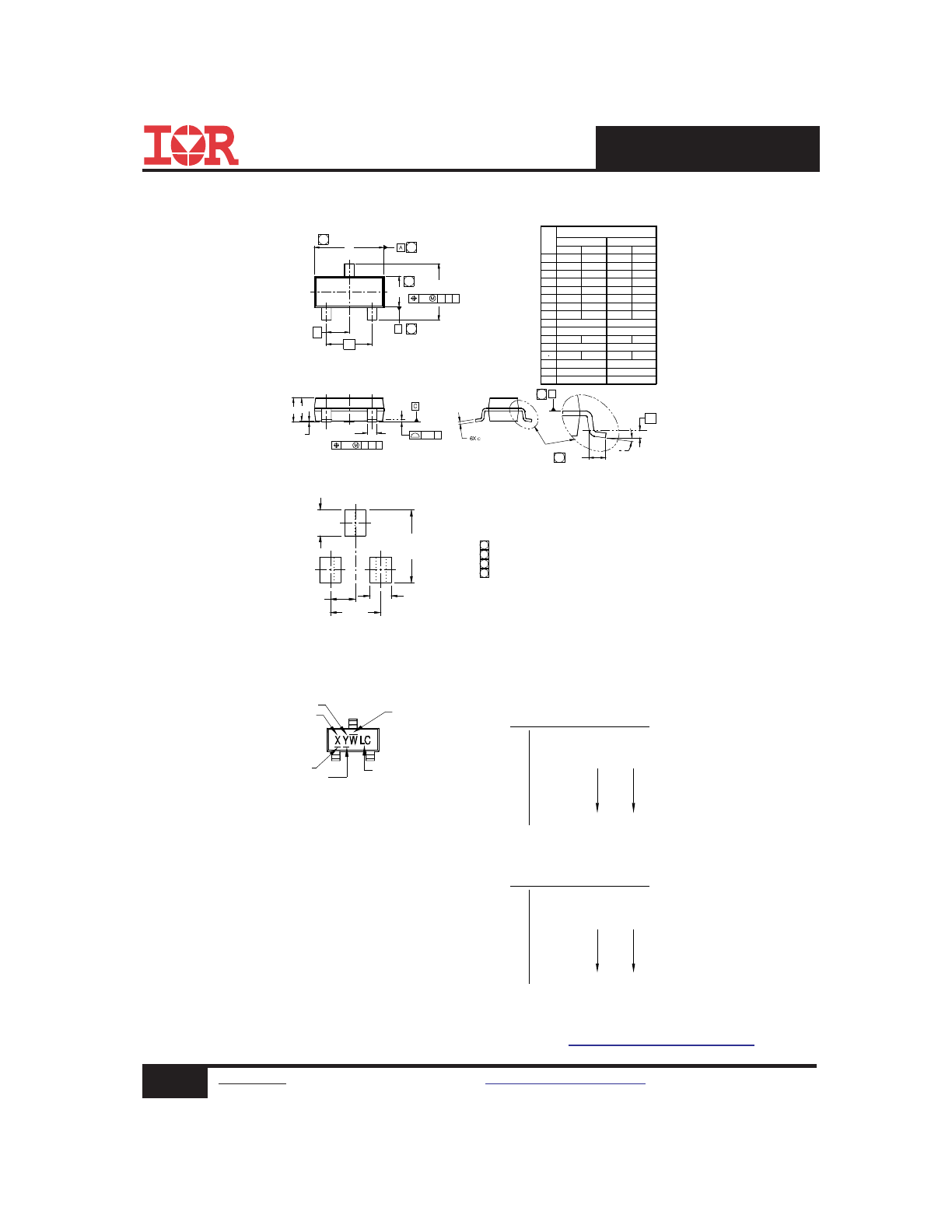
Micro3 (SOT-23 / TO-236AB) Part Marking Information
Micro3 (SOT-23) (Lead-Free) Package Outline
Dimensions are shown in millimeters (inches)
0.08
0.88
0.01
0.89
0.95 BSC
MILLIME TERS
MIN
e
E
E1
D
L
A
A1
A2
c
M
O
B
S
Y
MIN
MAX
MAX
.036
.0375 BSC
DIME NSIONS
INCHES
b
0.30
bbb
0.15
.008
ccc
.006
0.25 BS C
L1
L
0.40
0.60
.0118 BSC
aaa
0.20
.004
0°
8°
8°
0°
2.80
1.20
0
E1
E
D
5
6
3
1
2
ccc
C B A
B
5
6
e
e1
A2
A
A1
bbb
C A B
3X b
aaa C
3 S URF
0
3X L
L1
H
4
7
2.10
e1
1.90 BSC
.075 BSC
.0119
.0032
.111
.083
.048
.055
.119
.103
.0196
.0078
.0039
.044
.0004
.035
.040
.0236
.0158
1.02
0.20
0.50
2.64
3.04
1.40
1.12
0.10
0.10
1.90
[.075]
0.95
[.0375]
0.972
[.038]
2.742
[.1079]
0.802
[.031]
RECOMMENDED FOOTPRINT
3X
3X
NOT ES
1. DIMENSIONING AND T OLERANCING PER ASME Y14.5M-1994.
4 DATUM PLANE H IS LOCATED AT T HE MOLD PART ING LINE.
5 DATUM A AND B T O BE DET ERMINED AT DAT UM PLANE H.
6 DIMENSIONS D AND E1 ARE MEASURED AT DAT UM PLANE H.
2. DIMENSIONS ARE SHOWN IN MILLIMETERS AND INCHES.
3. CONT ROLLING DIMENSION: MILLIMET ER.
7 DIMENSION L IS T HE LEAD LENGTH FOR SOLDERING T O A SUBST RATE.
8. OUT LINE CONFORMS TO JEDEC OUT LINE T O-236AB.
F = IRLML6401
A
2001
A
27
Notes: This part marking information applies to devices produced after 02/26/2001
ASSEMBLY LOT CODE
LEAD-FREE
DATE CODE
E = IRLML6402
X = PART NUMBER CODE REFERENCE:
D = IRLML5103
C = IRLML6302
B = IRLML2803
A = IRLML2402
W = (1-26) IF PRECEDED BY LAST DIGIT OF CALENDAR YEAR
W = (27-52) IF PRECEDED BY A LETTER
Y
8
2008
3
2003
1
2001
YEAR
2002
2
5
2005
2004
4
2007
2006
7
6
2010
0
2009
9
YEAR
Y
C
03
WORK
WEEK
01
02
A
W
B
04
D
24
26
25
X
Z
Y
WORK
WEEK
W
H = IRLML5203
G = IRLML2502
K
H
G
F
E
D
C
B
2006
2003
2002
2005
2004
2008
2007
2010
2009
J
Y
51
29
28
30
C
B
D
50
X
I = IRLML0030
J = IRLML2030
L = IRLML0060
M = IRLML0040
K = IRLML0100
N = IRLML2060
P = IRLML9301
R = IRLML9303
Cu WIRE
HALOGEN FREE
PART NUMBER
52
Z
DATE CODE EXAMPLE:
YWW = 432 = DF
YWW = 503 = 5C
2018
2013
2011
2012
2015
2014
2017
2016
2020
2019
2018
2013
2011
2012
2015
2014
2017
2016
2020
2019
W = IRFML8244
V = IRLML6346
U = IRLML6344
T = IRLML6246
S = IRLML6244
Y = IRLML2246
X = IRLML2244
Z = IRFML9244
Note: For the most current drawing please refer to IR website at
http://www.irf.com/package
8
www.irf.com
©
2014 International Rectifier
Submit Datasheet Feedback
April 28, 2014
IRLML6402PbF
Micro3™(SOT-23/TO-263AB) Tape & Reel Information
Dimensions are shown in millimeters (inches)
2.05 ( .080 )
1.95 ( .077 )
TR
FEED DIRECTION
4.1 ( .161 )
3.9 ( .154 )
1.6 ( .062 )
1.5 ( .060 )
1.85 ( .072 )
1.65 ( .065 )
3.55 ( .139 )
3.45 ( .136 )
1.1 ( .043 )
0.9 ( .036 )
4.1 ( .161 )
3.9 ( .154 )
0.35 ( .013 )
0.25 ( .010 )
8.3 ( .326 )
7.9 ( .312 )
1.32 ( .051 )
1.12 ( .045 )
9.90 ( .390 )
8.40 ( .331 )
178.00
( 7.008 )
MAX.
NOTES:
1. CONTROLLING DIMENSION : MILLIMETER.
2. OUTLINE CONFORMS TO EIA-481 & EIA-541.
Note: For the most current drawing please refer to IR website at
http://www.irf.com/package
9
www.irf.com
©
2014 International Rectifier
Submit Datasheet Feedback
April 28, 2014
IRLML6402PbF
MS L1
(per JEDEC J-S TD-020D
††
)
RoHS compliant
Yes
Qualification information
†
Qualification level
Consumer
(per JEDEC JES D47F
††
guidelines)
Moisture Sensitivity Level
Micro3
™ (SOT-23)
† Qualification standards can be found at International Rectifier’s web site:
http://www.irf.com/product-info/reliability
††
Applicable version of JEDEC standard at the time of product release
IR WORLD HEADQUARTERS: 101 N. Sepulveda Blvd., El Segundo, California 90245, USA
To contact International Rectifier, please visit
http://www.irf.com/whoto-call/
Revision History
Date
Comment
• Updated data sheet with new IR corporate template.
• Updated package outline & part marking on page 7.
• Added Qualification table -Qual level "Consumer" on page 9.
• Added bullet point in the Benefits "RoHS Compliant, Halogen -Free" on page 1.
4/28/2014