
10/12/12
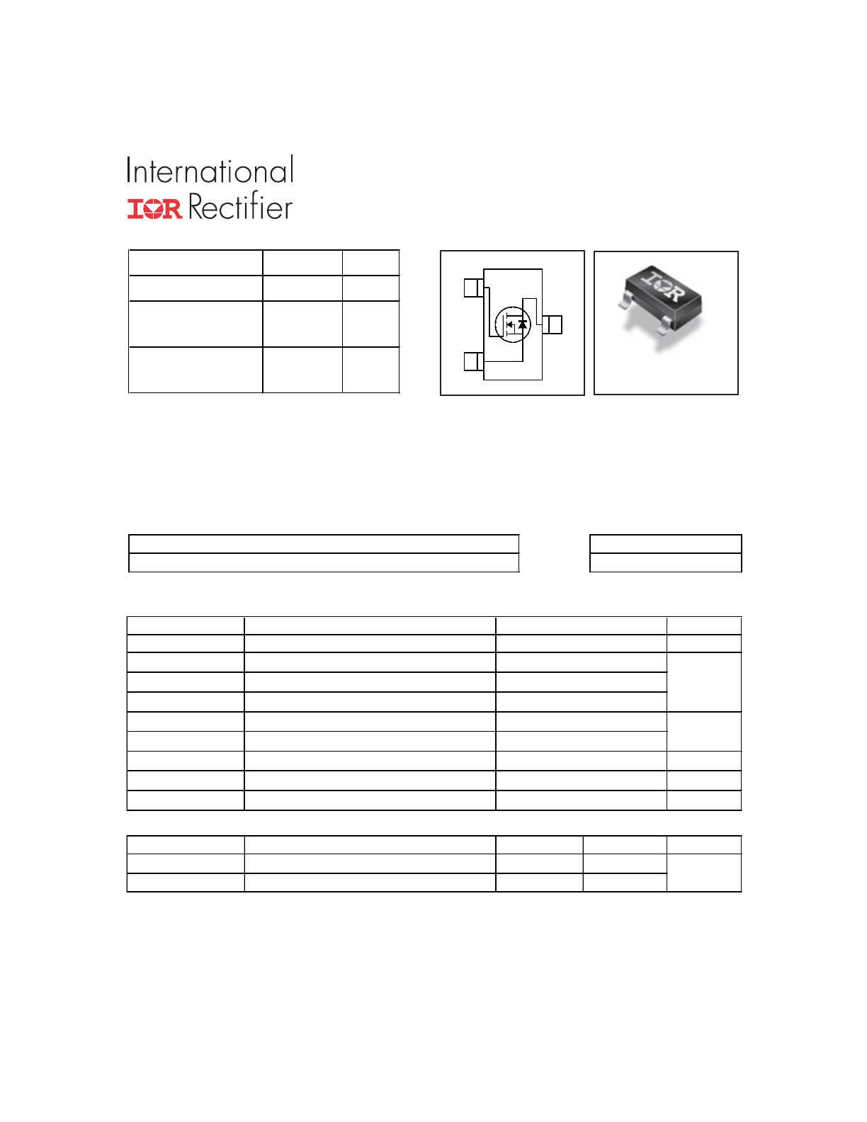
IRLML6246TRPbF
HEXFET
®
Power MOSFET
www.irf.com
1
ORDERING INFORMATION:
See detailed ordering and shipping information on the last page of this data sheet.
Notes
through
are on page 10
Application(s)
Micro3
TM
(SOT-23)
IRLML6246TRPbF
D
S
G
3
1
2
• Load/ System Switch
Features and Benefits
Features
Benefits
V
DS
20
V
V
GS Max
± 12
V
R
DS(on) max
(@V
GS
= 4.5V)
46
m
:
R
DS(on) max
(@V
GS
= 2.5V)
66
m
:
Absolute Maximum Ratings
Symbol
Parameter
Units
V
DS
Drain-Source Voltage
V
I
D
@ T
A
= 25°C
Continuous Drain Current, V
GS
@ 10V
I
D
@ T
A
= 70°C
Continuous Drain Current, V
GS
@ 10V
I
DM
Pulsed Drain Current
P
D
@T
A
= 25°C
Maximum Power Dissipation
P
D
@T
A
= 70°C
Maximum Power Dissipation
Linear Derating Factor
W/°C
V
GS
Gate-to-Source Voltage
V
T
J,
T
STG
Junction and Storage Temperature Range
°C
Thermal Resistance
Symbol
Parameter
Typ.
Max.
Units
R
θJA
Junction-to-Ambient
e
–––
100
R
θJA
Junction-to-Ambient (t<10s)
f
–––
99
W
°C/W
A
Max.
4.1
3.3
-55 to + 150
± 12
0.01
20
1.3
0.8
16
Industry-standard SOT-23 Package
Multi-vendor compatibility
RoHS compliant containing no lead, no bromide and no halogen
results in
Environmentally friendly
PD - 97529A
IRLML6246TRPbF
2
www.irf.com
D
S
G
Electric Characteristics @ T
J
= 25°C (unless otherwise specified)
Symbol
Parameter
Min. Typ. Max. Units
V
(BR)DSS
Drain-to-Source Breakdown Voltage
20
–––
–––
V
ΔV
(BR)DSS
/
ΔT
J
Breakdown Voltage Temp. Coefficient
–––
0.03
–––
V/°C
–––
30
46
–––
45
66
V
GS(th)
Gate Threshold Voltage
0.5
0.8
1.1
V
I
DSS
–––
–––
1.0
–––
–––
10
–––
–––
150
I
GSS
Gate-to-Source Forward Leakage
–––
–––
100
Gate-to-Source Reverse Leakage
–––
–––
-100
R
G
Internal Gate Resistance
–––
4.0
–––
Ω
gfs
Forward Transconductance
10
–––
–––
S
Q
g
Total Gate Charge
–––
3.5
–––
Q
gs
Gate-to-Source Charge
–––
0.26
–––
Q
gd
Gate-to-Drain ("Miller") Charge
–––
1.7
–––
t
d(on)
Turn-On Delay Time
–––
3.6
–––
t
r
Rise Time
–––
4.9
–––
t
d(off)
Turn-Off Delay Time
–––
11
–––
t
f
Fall Time
–––
6.0
–––
C
iss
Input Capacitance
–––
290
–––
C
oss
Output Capacitance
–––
64
–––
C
rss
Reverse Transfer Capacitance
–––
41
–––
Source - Drain Ratings and Characteristics
Symbol
Parameter
Min. Typ. Max. Units
I
S
Continuous Source Current
(Body Diode)
I
SM
Pulsed Source Current
(Body Diode)
c
V
SD
Diode Forward Voltage
–––
–––
1.2
V
t
rr
Reverse Recovery Time
–––
8.6
13
ns
Q
rr
Reverse Recovery Charge
–––
2.8
4.2
nC
I
D
= 1.0A
T
J
= 25°C, V
R
= 15V, I
F
=1.3A
V
DS
= 16V, V
GS
= 0V, T
J
= 55°C
V
DS
= 16V
ƒ = 1.0MHz
R
G
= 6.8
Ω
V
GS
= 4.5V
d
di/dt = 100A/μs
d
V
GS
= 12V
V
GS
= -12V
T
J
= 25°C, I
S
= 4.1A, V
GS
= 0V
d
integral reverse
p-n junction diode.
Conditions
V
GS
= 0V, I
D
= 250μA
Reference to 25°C, I
D
= 1mA
V
GS
= 4.5V, I
D
=
4.1A
d
MOSFET symbol
showing the
V
DS
=10V
Conditions
V
GS
= 4.5V
V
GS
= 0V
R
DS(on)
V
GS
= 2.5V, I
D
=
3.3A
d
Static Drain-to-Source On-Resistance
Drain-to-Source Leakage Current
μA
m
Ω
V
DD
=10V
d
nA
nC
ns
V
DS
= V
GS
, I
D
= 5μA
V
DS
=16V, V
GS
= 0V
V
DS
= 16V, V
GS
= 0V, T
J
= 125°C
V
DS
= 10V, I
D
= 4.1A
I
D
= 4.1A
–––
–––
–––
–––
pF
A
1.3
16
IRLML6246TRPbF
www.irf.com
3
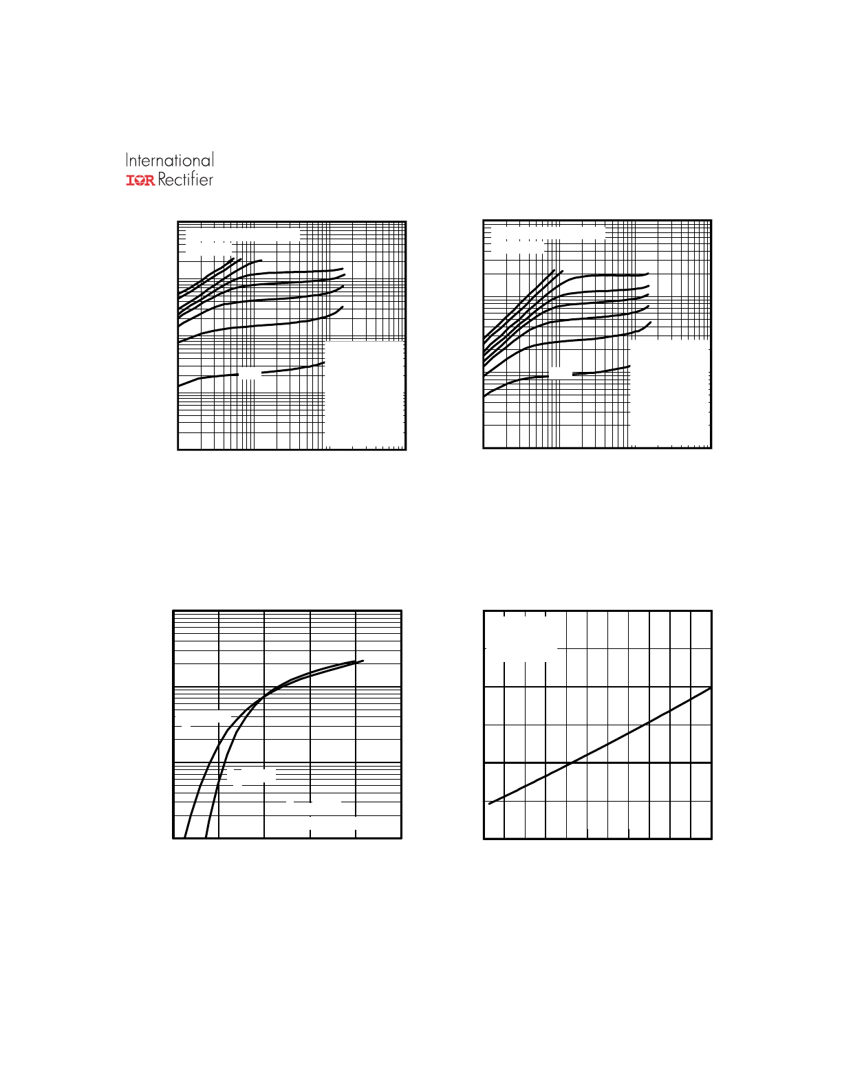
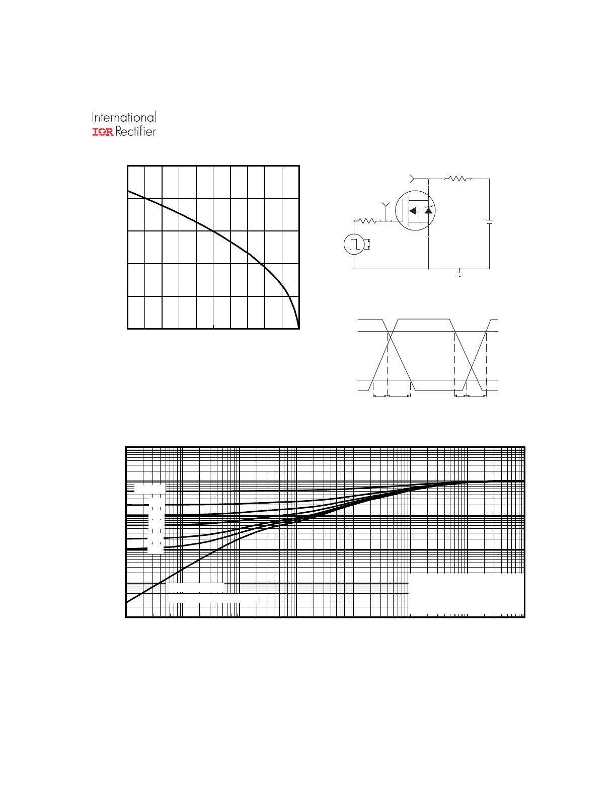
Fig 3. Typical Transfer Characteristics
Fig 2. Typical Output Characteristics
Fig 1. Typical Output Characteristics
Fig 4. Normalized On-Resistance
Vs. Temperature
0.1
1
10
100
VDS, Drain-to-Source Voltage (V)
0.01
0.1
1
10
100
I D
, D
ra
in
-t
o-
S
ou
rc
e
C
ur
re
nt
(
A
)
≤60μs PULSE WIDTH
Tj = 25°C
1.5V
VGS
TOP
10V
4.5V
3.0V
2.5V
2.3V
2.0V
1.8V
BOTTOM
1.5V
0.1
1
10
100
VDS, Drain-to-Source Voltage (V)
0.1
1
10
100
I D
, D
ra
in
-t
o-
S
ou
rc
e
C
ur
re
nt
(
A
)
≤60μs PULSE WIDTH
Tj = 150°C
1.5V
VGS
TOP
10V
4.5V
3.0V
2.5V
2.3V
2.0V
1.8V
BOTTOM
1.5V
1.0
1.5
2.0
2.5
3.0
3.5
VGS, Gate-to-Source Voltage (V)
0.1
1
10
100
I D
, D
ra
in
-t
o-
S
ou
rc
e
C
ur
re
nt
(
A
)
TJ = 25°C
TJ = 150°C
VDS = 15V
≤60μs PULSE WIDTH
-60 -40 -20 0 20 40 60 80 100 120 140 160
TJ , Junction Temperature (°C)
0.5
1.0
1.5
2.0
R
D
S
(o
n)
,
D
ra
in
-t
o-
S
ou
rc
e
O
n
R
es
is
ta
nc
e
(
N
or
m
al
iz
ed
)
ID = 4.1A
VGS = 4.5V
IRLML6246TRPbF
4
www.irf.com
Fig 6. Typical Gate Charge Vs.
Gate-to-Source Voltage
Fig 5. Typical Capacitance Vs.
Drain-to-Source Voltage
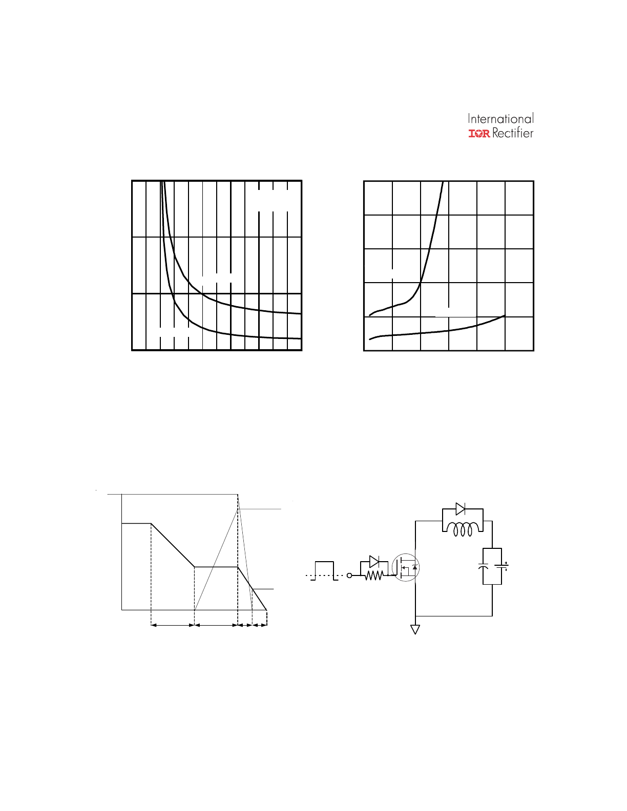
Fig 8. Maximum Safe Operating Area
Fig 7. Typical Source-Drain Diode
Forward Voltage
1
10
100
VDS, Drain-to-Source Voltage (V)
10
100
1000
10000
C
, C
ap
ac
ita
nc
e
(p
F
)
VGS = 0V, f = 1 MHZ
Ciss = Cgs + Cgd, C ds SHORTED
Crss = Cgd
Coss = Cds + Cgd
Coss
Crss
Ciss
0.2
0.4
0.6
0.8
1.0
1.2
VSD, Source-to-Drain Voltage (V)
0.0
0
1
10
100
I S
D
, R
ev
er
se
D
ra
in
C
ur
re
nt
(
A
)
TJ = 25°C
TJ = 150°C
VGS = 0V
0.1
1
10
100
VDS, Drain-to-Source Voltage (V)
0.01
0.1
1
10
100
I D
,
D
ra
in
-t
o-
S
ou
rc
e
C
ur
re
nt
(
A
)
TA = 25°C
Tj = 150°C
Single Pulse
1msec
10msec
OPERATION IN THIS AREA
LIMITED BY RDS(on)
100μsec
0.0
2.0
4.0
6.0
8.0
QG, Total Gate Charge (nC)
0.0
2.0
4.0
6.0
8.0
10.0
12.0
14.0
V
G
S
, G
at
e-
to
-S
ou
rc
e
V
ol
ta
ge
(
V
)
VDS= 16V
VDS= 10V
VDS= 4.0V
ID= 4.1A
IRLML6246TRPbF
www.irf.com
5
Fig 11. Typical Effective Transient Thermal Impedance, Junction-to-Ambient
Fig 9. Maximum Drain Current Vs.
Ambient Temperature
V
DS
90%
10%
V
GS
t
d(on)
t
r
t
d(off)
t
f
Fig 10b. Switching Time Waveforms
Fig 10a. Switching Time Test Circuit
V
DS
Pulse Width ≤ 1 µs
Duty Factor ≤ 0.1 %
R
D
V
GS
R
G
D.U.T.
V
GS
+
-
V
DD
25
50
75
100
125
150
TA , Ambient Temperature (°C)
0.0
1.0
2.0
3.0
4.0
5.0
I D
,
D
ra
in
C
ur
re
nt
(
A
)
1E-006
1E-005
0.0001
0.001
0.01
0.1
1
10
t1 , Rectangular Pulse Duration (sec)
0.01
0.1
1
10
100
1000
T
he
rm
al
R
es
po
ns
e
(
Z
th
JA
)
0.20
0.10
D = 0.50
0.02
0.01
0.05
SINGLE PULSE
( THERMAL RESPONSE )
Notes:
1. Duty Factor D = t1/t2
2. Peak Tj = P dm x Zthjc + Tc
IRLML6246TRPbF
6
www.irf.com
Fig 13. Typical On-Resistance Vs. Drain
Current
Fig 12. Typical On-Resistance Vs. Gate
Voltage
Fig 14b. Gate Charge Test Circuit
Fig 14a. Basic Gate Charge Waveform
1K
VCC
DUT
0
L
S
20K
Vds
Vgs
Id
Vgs(th)
Qgs1
Qgs2
Qgd
Qgodr
0
5
10
15
20
25
30
ID, Drain Current (A)
20
40
60
80
100
120
R
D
S
(o
n)
,
D
ra
in
-t
o
-S
ou
rc
e
O
n
R
es
is
ta
nc
e
(
m
Ω
)
Vgs = 10V
Vgs = 4.5V
0
1
2
3
4
5
6
7
8
9 10 11 12
VGS, Gate -to -Source Voltage (V)
20
40
60
80
R
D
S
(o
n)
,
D
ra
in
-t
o
-S
ou
rc
e
O
n
R
es
is
ta
nc
e
(m
Ω
)
ID = 4.1A
TJ = 25°C
TJ = 125°C
IRLML6246TRPbF
www.irf.com
7
Fig 15. Typical Threshold Voltage Vs.
Junction Temperature
Fig 16. Typical Power Vs. Time
-75 -50 -25
0
25
50
75 100 125 150
TJ , Temperature ( °C )
0.0
0.5
1.0
1.5
V
G
S
(t
h)
, G
at
e
th
re
sh
ol
d
V
ol
ta
ge
(
V
)
ID = 10uA
ID = 250uA
1E-005 0.0001
0.001
0.01
0.1
1
10
Time (sec)
0
20
40
60
80
100
P
ow
er
(
W
)
IRLML6246TRPbF
8
www.irf.com
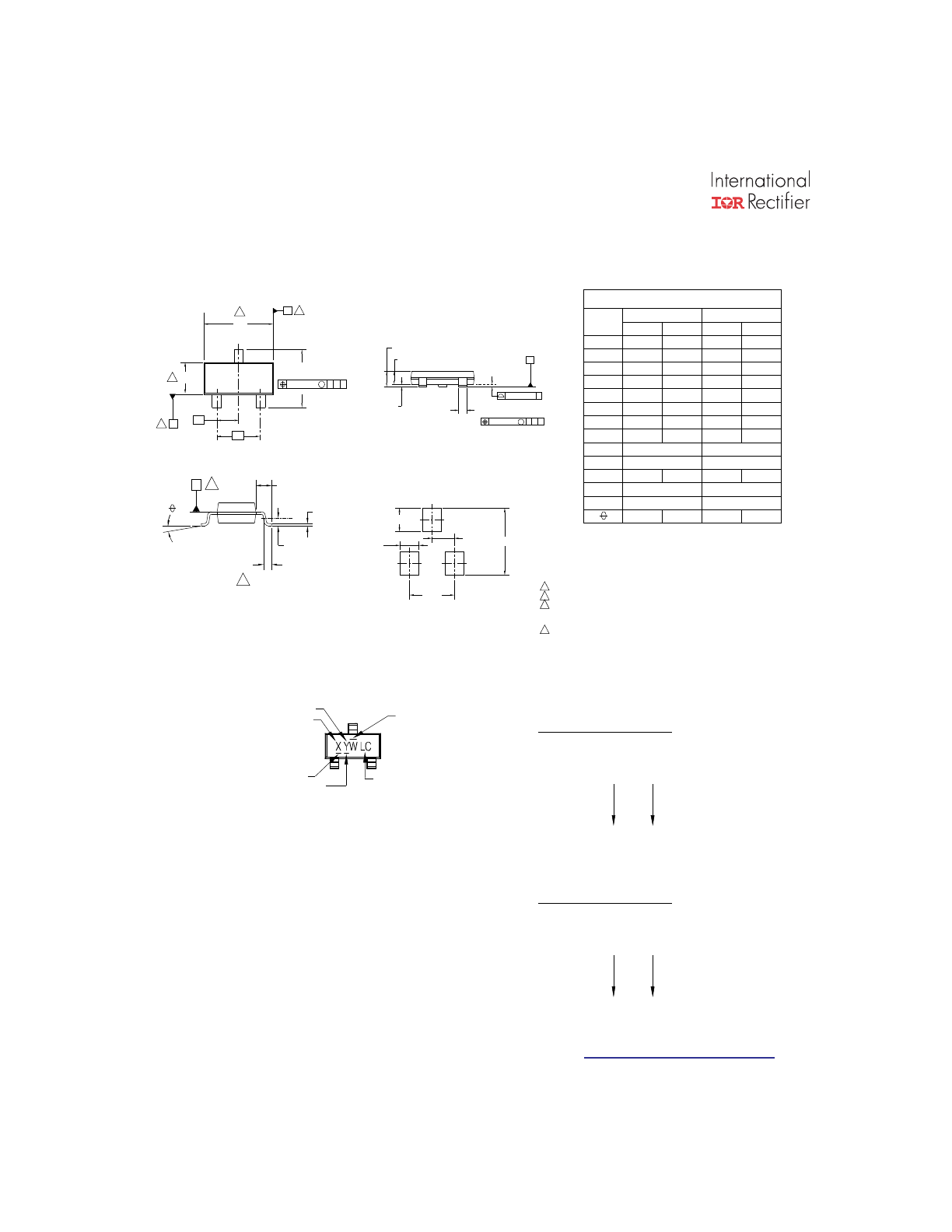
Micro3™(SOT-23) Part Marking Information
Micro3™(SOT-23) Package Outline
Dimensions are shown in millimeters (inches)
Note: For the most current drawing please refer to IR website at:
http://www.irf.com/package/
e
E1
E
D
A
B
0.15 [0.006]
e1
1
2
3
M C B A
5
6
6
5
NOTES:
b
A1
3X
A
A2
A
B
C
M
0.20 [0.008]
0.10 [0.004] C
C
1. DIMENSIONING & TOLERANCING PER ANSI Y14.5M-1994
2. DIMENSIONS ARE SHOWN IN MILLIMETERS [INCHES].
3. CONTROLLING DIMENSION: MILLIMETER.
4. DATUM PLANE H IS LOCATED AT THE MOLD PARTING LINE.
5. DATUM A AND B TO BE DETERMINED AT DATUM PLANE H.
6. DIMENSIONS D AND E1 ARE MEASURED AT DATUM PLANE H. DIMENSIONS DOES
NOT INCLUDE MOLD PROTRUSIONS OR INTERLEAD FLASH. MOLD PROTRUSIONS
OR INTERLEAD FLASH SHALL NOT EXCEED 0.25 MM [0.010 INCH] PER SIDE.
7. DIMENSION L IS THE LEAD LENGTH FOR SOLDERING TO A SUBSTRATE.
8. OUTLINE CONFORMS TO JEDEC OUTLINE TO-236 AB.
0.89
1.12
SYMBOL
MAX
MIN
A1
b
0.01
0.10
c
0.30
0.50
D
0.08
0.20
E
2.80
3.04
E1
2.10
2.64
e
1.20
1.40
A
0.95
BSC
L
0.40
0.60
0
8
MILLIMETERS
A2
0.88
1.02
e1
1.90
BSC
REF
0.54
L1
BSC
0.25
L2
BSC
REF
%6&
INCHES
8
0
%6&
0.0004
MIN
MAX
DIMENSIONS
0.972
1.900
Recommended Footprint
0.802
0.950
2.742
3X L
c
L2
H 4
L1
7
F = IRLML6401
A
2001
A
27
LOT CODE
LEAD FREE
DATE CODE
E = IRLML6402
X = PART NUMBER CODE REFERENCE:
D = IRLML5103
C = IRLML6302
B = IRLML2803
A = IRLML2402
W = (1-26) IF PRECEDED BY LAST DIGIT OF CALENDAR YEAR
W = (27-52) IF PRECEDED BY A LETTER
Y
8
2008
3
2003
1
2001
YEAR
2002
2
5
2005
2004
4
2007
2006
7
6
2010
0
2009
9
YEAR
Y
C
03
WORK
WEEK
01
02
A
W
B
04
D
24
26
25
X
Z
Y
WORK
WEEK
W
H = IRLML5203
G = IRLML2502
K
H
G
F
E
D
C
B
2006
2003
2002
2005
2004
2008
2007
2010
2009
J
Y
51
29
28
30
C
B
D
50
X
52
Z
Note: A line above the work week
(as shown here) indicates Lead - Free.
S = IRLML6244
T = IRLML6246
U= IRLML6344
V = IRLML6346
I = IRLML0030
J = IRLML2030
L = IRLML0060
M = IRLML0040
K = IRLML0100
N = IRLML2060
P = IRLML9301
R = IRLML9303
Cu WIRE
HALOGEN FREE
PART NUMBER
IRLML6246TRPbF
www.irf.com
9
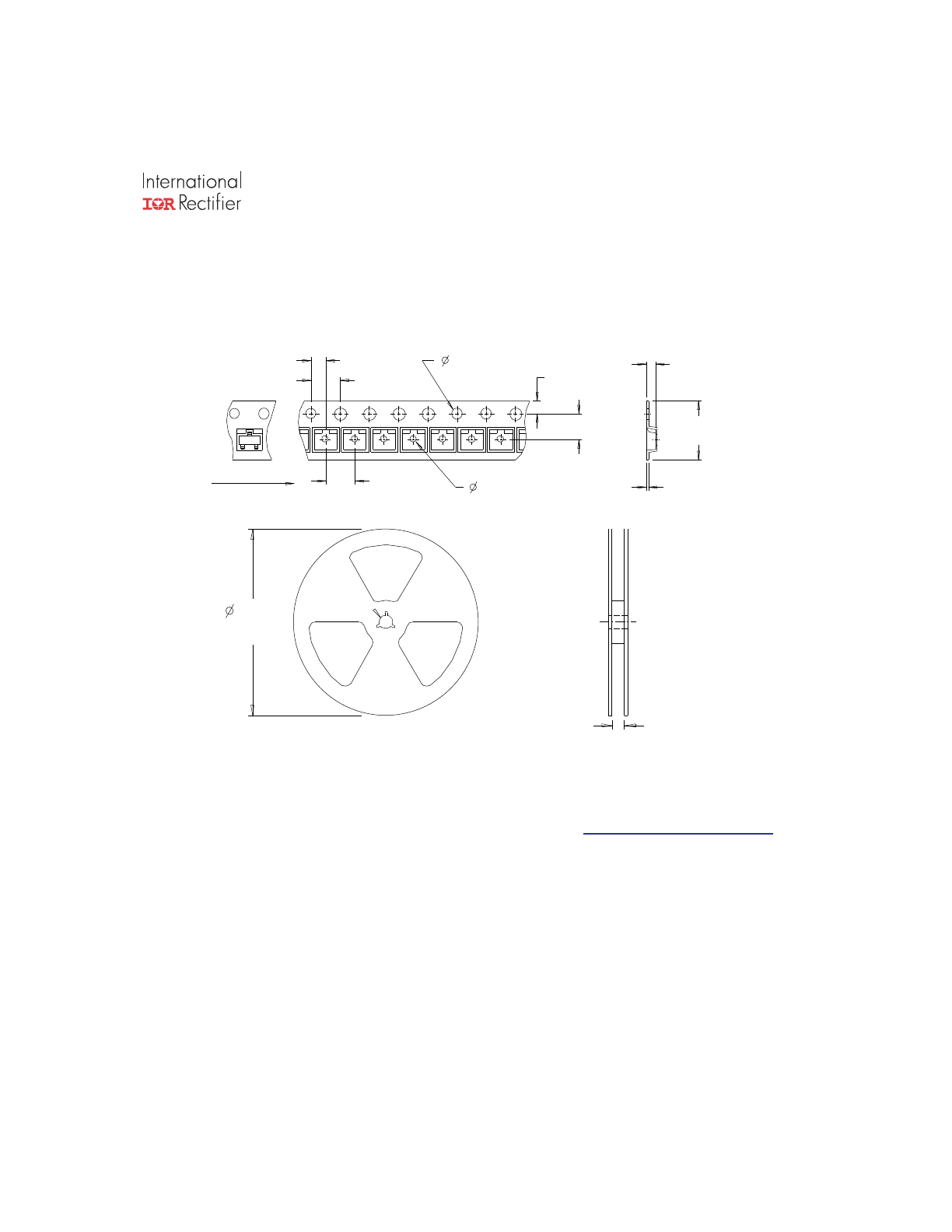
Micro3™(SOT-23) Tape & Reel Information
Dimensions are shown in millimeters (inches)
2.05 ( .080 )
1.95 ( .077 )
TR
FEED DIRECTION
4.1 ( .161 )
3.9 ( .154 )
1.6 ( .062 )
1.5 ( .060 )
1.85 ( .072 )
1.65 ( .065 )
3.55 ( .139 )
3.45 ( .136 )
1.1 ( .043 )
0.9 ( .036 )
4.1 ( .161 )
3.9 ( .154 )
0.35 ( .013 )
0.25 ( .010 )
8.3 ( .326 )
7.9 ( .312 )
1.32 ( .051 )
1.12 ( .045 )
9.90 ( .390 )
8.40 ( .331 )
178.00
( 7.008 )
MAX.
NOTES:
1. CONTROLLING DIMENSION : MILLIMETER.
2. OUTLINE CONFORMS TO EIA-481 & EIA-541.
Note: For the most current drawing please refer to IR website at:
http://www.irf.com/package/
IRLML6246TRPbF
10
www.irf.com
Data and specifications subject to change without notice.
IR WORLD HEADQUARTERS: 101N. Sepulveda blvd, El Segundo, California 90245, USA Tel: (310) 252-7105
TAC Fax: (310) 252-7903
Visit us at www.irf.com for sales contact information.10/2012
Qualification standards can be found at International Rectifier’s web site
http://www.irf.com/product-info/reliability
Higher qualification ratings may be available should the user have such requirements.
Please contact your International Rectifier sales representative for further information:
http://www.irf.com/whoto-call/salesrep/
Applicable version of JEDEC standard at the time of product release.
Notes:
Repetitive rating; pulse width limited by max. junction temperature.
Pulse width ≤ 400μs; duty cycle ≤ 2%.
Surface mounted on 1 in square Cu board
Refer to
application note #AN-994.
MSL1
(per IPC/JEDEC J-STD-020D
†††
)
RoHS compliant
Yes
Micro3
™(SOT-23)
Qualification information
†
Moisture Sensitivity Level
Qualification level
Consumer
††
(per JEDEC JESD47F
†††
guidelines )
Note
Form
Quantity
IRLML6246TRPbF
Micro3™(SOT-23)
Tape and Reel
3000
Orderable part number
Package Type
Standard Pack
Date
Comments
10/12/2012
Added IDSS @ 16V, T
J
= 55C-pg2
Revision History