
Parameter
Max.
Units
V
DS
Drain- Source Voltage
-30
V
I
D
@ T
A
= 25°C
Continuous Drain Current, V
GS
@ -10V
-3.0
I
D
@ T
A
= 70°C
Continuous Drain Current, V
GS
@ -10V
-2.4
A
I
DM
Pulsed Drain Current
-24
P
D
@T
A
= 25°C
Power Dissipation
1.25
P
D
@T
A
= 70°C
Power Dissipation
0.80
Linear Derating Factor
10
mW/°C
V
GS
Gate-to-Source Voltage
± 20
V
T
J,
T
STG
Junction and Storage Temperature Range
-55 to + 150
°C
Parameter
Max.
Units
R
θJA
Maximum Junction-to-Ambient
100
°C/W
Thermal Resistance
Absolute Maximum Ratings
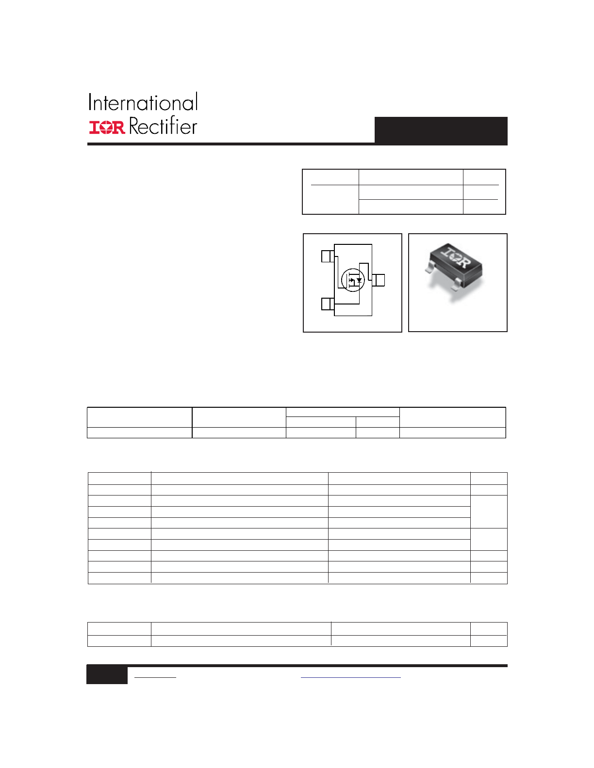
W
HEXFET
®
Power MOSFET
These P-channel MOSFETs from International Rectifier utilize
advanced processing techniques to achieve the extremely low
on-resistance per silicon area. This benefit provides the
designer with an extremely efficient device for use in battery
and load management applications.
A thermally enhanced large pad leadframe has been
incorporated into the standard SOT-23 package to produce a
HEXFET Power MOSFET with the industry's smallest footprint.
This package, dubbed the Micro3
TM
, is ideal for applications
where printed circuit board space is at a premium. The low
profile (<1.1mm) of the Micro3 allows it to fit easily into
extremely thin application environments such as portable
electronics and PCMCIA cards. The thermal resistance and
power dissipation are the best available.
Description
l
Ultra Low On-Resistance
l
P-Channel MOSFET
l
Surface Mount
l
Available in Tape & Reel
l
Low Gate Charge
l
Lead-Free
l
RoHS Compliant, Halogen-Free
V
DSS
R
DS(on)
max (m
W)
I
D
-30V
98@V
GS
= -10V
-3.0A
165@V
GS
= -4.5V
-2.6A
S
G 1
2
D
3
Micro3
TM
IRLML5203PbF
Form
Quantity
IRLML5203TRPbF
Micro3™ (SOT-23)
Tape and Reel
3000
IRLML5203TRPbF
Package Type
Standard Pack
Orderable Part Number
Base Part Number
1
www.irf.com
©
2014 International Rectifier
Submit Datasheet Feedback
April 28, 2014
2
www.irf.com
©
2014 International Rectifier
Submit Datasheet Feedback
April 28, 2014
IRLML5203PbF
Parameter
Min. Typ. Max. Units
Conditions
I
S
Continuous Source Current
MOSFET symbol
(Body Diode)
showing the
I
SM
Pulsed Source Current
integral reverse
(Body Diode)
p-n junction diode.
V
SD
Diode Forward Voltage
––– ––– -1.2
V
T
J
= 25°C, I
S
= -1.3A, V
GS
= 0V
t
rr
Reverse Recovery Time
–––
17
26
ns
T
J
= 25°C, I
F
= -1.3A
Q
rr
Reverse Recovery Charge
–––
12
18
nC
di/dt = -100A/μs
Source-Drain Ratings and Characteristics
A
-24
-1.3
S
D
G
Repetitive rating; pulse width limited by
max. junction temperature.
Notes:
Pulse width ≤ 400μs; duty cycle ≤ 2%.
Surface mounted on FR-4 board, t ≤ 5sec.
Parameter
Min. Typ. Max. Units
Conditions
V
(BR)DSS
Drain-to-Source Breakdown Voltage
-30
––– –––
V
V
GS
= 0V, I
D
= -250μA
ΔV
(BR)DSS
/
ΔT
J
Breakdown Voltage Temp. Coefficient
––– 0.019 –––
V/°C Reference to 25°C, I
D
= -1mA
–––
–––
98
V
GS
= -10V, I
D
= -3.0A
–––
––– 165
V
GS
= -4.5V, I
D
= -2.6A
V
GS(th)
Gate Threshold Voltage
-1.0 ––– -2.5
V
V
DS
= V
GS
, I
D
= -250μA
g
fs
Forward Transconductance
3.1
––– –––
S
V
DS
= -10V, I
D
= -3.0A
–––
––– -1.0
V
DS
= -24V, V
GS
= 0V
–––
––– -5.0
V
DS
= -24V, V
GS
= 0V, T
J
= 70°C
Gate-to-Source Forward Leakage
–––
––– -100
V
GS
= -20V
Gate-to-Source Reverse Leakage
–––
––– 100
V
GS
= 20V
Q
g
Total Gate Charge
–––
9.5
14
I
D
= -3.0A
Q
gs
Gate-to-Source Charge
–––
2.3
3.5
nC
V
DS
= -24V
Q
gd
Gate-to-Drain ("Miller") Charge
–––
1.6
2.4
V
GS
= -10V
t
d(on)
Turn-On Delay Time
–––
12
–––
V
DD
= -15V
t
r
Rise Time
–––
18
–––
I
D
= -1.0A
t
d(off)
Turn-Off Delay Time
–––
88
–––
R
G
= 6.0
Ω
t
f
Fall Time
–––
52
–––
V
GS
= -10V
C
iss
Input Capacitance
–––
510 –––
V
GS
= 0V
C
oss
Output Capacitance
–––
71
–––
pF
V
DS
= -25V
C
rss
Reverse Transfer Capacitance
–––
43
–––
ƒ = 1.0MHz
Electrical Characteristics @ T
J
= 25°C (unless otherwise specified)
I
GSS
µA
m
Ω
R
DS(on)
Static Drain-to-Source On-Resistance
I
DSS
Drain-to-Source Leakage Current
nA
ns
3
www.irf.com
©
2014 International Rectifier
Submit Datasheet Feedback
April 28, 2014
IRLML5203PbF
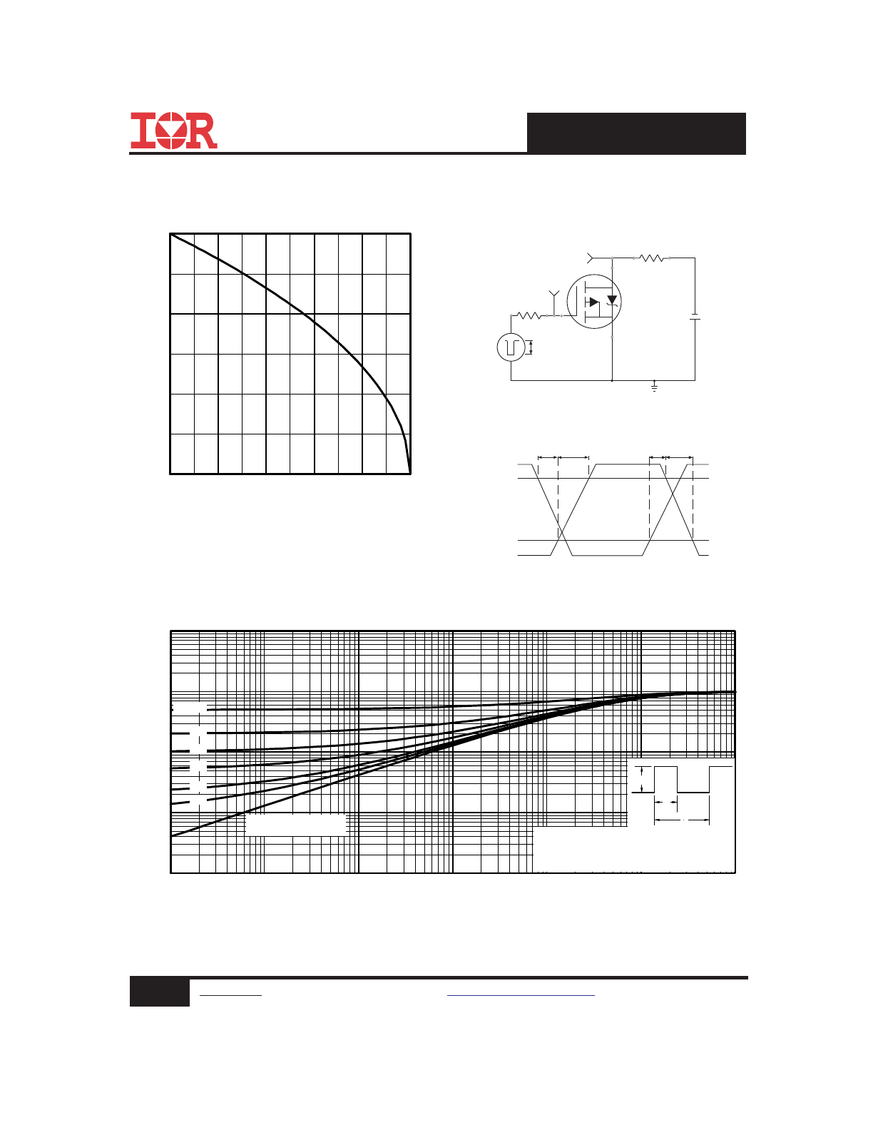
Fig 4. Normalized On-Resistance
Vs. Temperature
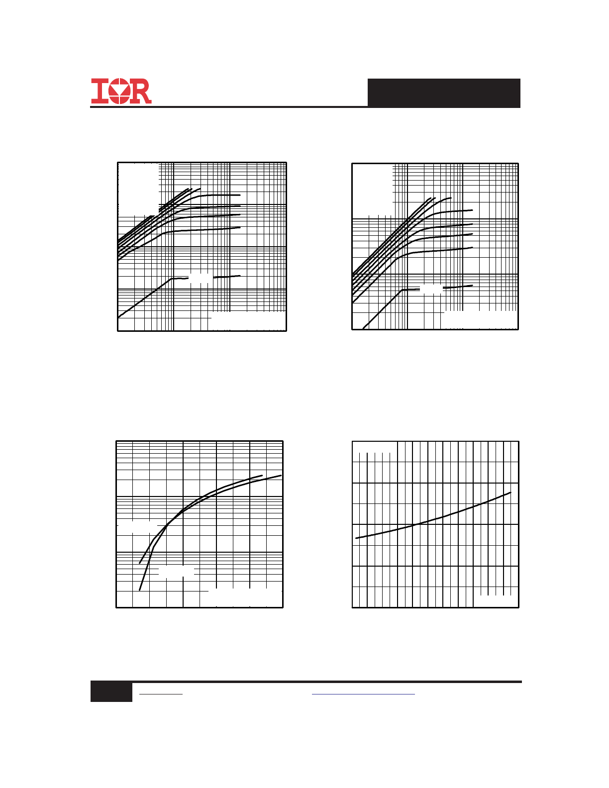
Fig 2. Typical Output Characteristics
Fig 1. Typical Output Characteristics
Fig 3. Typical Transfer Characteristics
-60 -40 -20
0
20 40 60 80 100 120 140 160
0.0
0.5
1.0
1.5
2.0
T , Junction Temperature ( C)
R , Drain-to-Source On Resistance
(Normalized)
J
D
S
(on)
°
V
=
I =
GS
D
-10V
3.0A
0.01
0.1
1
10
100
0.1
1
10
100
20μs PULSE WIDTH
T = 25 C
J
°
TOP
BOTTOM
VGS
-15V
-10V
-7.0V
-5.5V
-4.5V
-4.0V
-3.5V
-2.7V
-V , Drain-to-Source Voltage (V)
-I , Drain-to-Source Current (A)
DS
D
-2.70V
0.1
1
10
100
0.1
1
10
100
20μs PULSE WIDTH
T = 150 C
J
°
TOP
BOTTOM
VGS
-15V
-10V
-7.0V
-5.5V
-4.5V
-4.0V
-3.5V
-2.7V
-V , Drain-to-Source Voltage (V)
-I , Drain-to-Source Current (A)
DS
D
-2.70V
0.1
1
10
100
2.0
3.0
4.0
5.0
6.0
7.0
V = -15V
20μs PULSE WIDTH
DS
-V , Gate-to-Source Voltage (V)
-I , Drain-to-Source Current (A)
GS
D
T = 25 C
J
°
T = 150 C
J
°
4
www.irf.com
©
2014 International Rectifier
Submit Datasheet Feedback
April 28, 2014
IRLML5203PbF
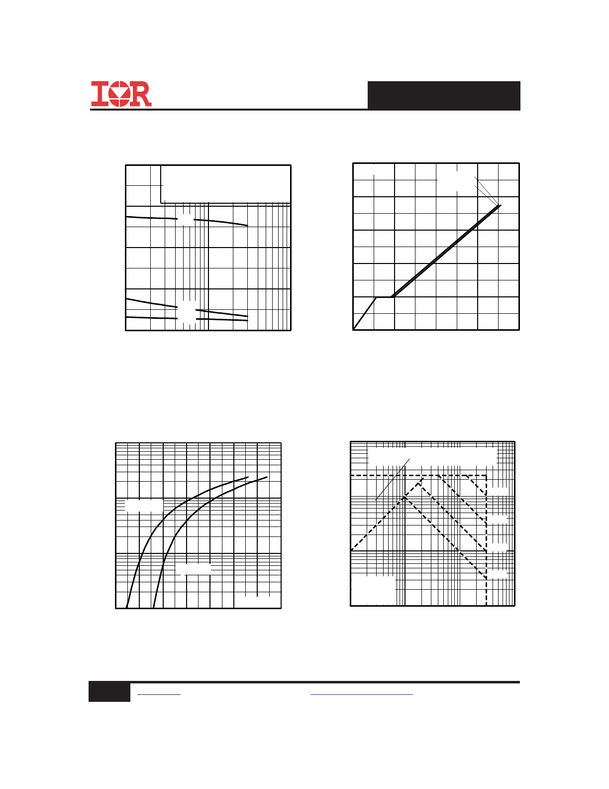
Fig 8. Maximum Safe Operating Area
Fig 6. Typical Gate Charge Vs.
Gate-to-Source Voltage
Fig 5. Typical Capacitance Vs.
Drain-to-Source Voltage
Fig 7. Typical Source-Drain Diode
Forward Voltage
0
4
8
12
16
0
4
8
12
16
20
Q , Total Gate Charge (nC)
-V , Gate-to-Source Voltage (V)
G
GS
I =
D
-3.0A
V
=-15V
DS
V
=-24V
DS
0.1
1
10
100
0.4
0.6
0.8
1.0
1.2
1.4
1.6
1.8
-V ,Source-to-Drain Voltage (V)
-I , Reverse Drain Current (A)
SD
SD
V = 0 V
GS
T = 25 C
J
°
T = 150 C
J
°
0.1
1
10
100
0.1
1
10
100
OPERATION IN THIS AREA LIMITED
BY R
DS(on)
Single Pulse
T
T
= 150 C
= 25 C
°
°
J
A
-V , Drain-to-Source Voltage (V)
-I , Drain Current (A)I , Drain Current (A)
DS
D
10us
100us
1ms
10ms
1
10
100
0
200
400
600
800
-V , Drain-to-Source Voltage (V)
C, Capacitance (pF)
DS
V
C
C
C
=
=
=
=
0V,
C
C
C
f = 1MHz
+ C
+ C
C SHORTED
GS
iss
gs
gd ,
ds
rss
gd
oss
ds
gd
C
iss
C
oss
C
rss
5
www.irf.com
©
2014 International Rectifier
Submit Datasheet Feedback
April 28, 2014
IRLML5203PbF
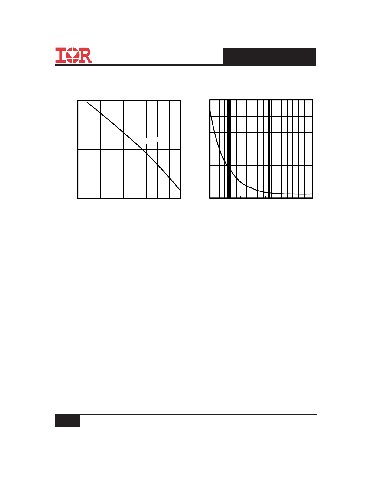
Fig 11. Maximum Effective Transient Thermal Impedance, Junction-to-Ambient
Fig 9. Maximum Drain Current Vs.
Case Temperature
25
50
75
100
125
150
0.0
1.0
2.0
3.0
T , Case Temperature ( C)
-I , Drain Current (A)
°
C
D
0.1
1
10
100
1000
0.00001
0.0001
0.001
0.01
0.1
1
10
Notes:
1. Duty factor D = t / t
2. Peak T = P
x Z
+ T
1
2
J
DM
thJA
A
P
t
t
DM
1
2
t , Rectangular Pulse Duration (sec)
Ther
m
al
R
esponse
(Z
)
1
th
JA
0.01
0.02
0.05
0.10
0.20
D = 0.50
SINGLE PULSE
(THERMAL RESPONSE)
V
DS
V
GS
Pulse Width ≤ 1 µs
Duty Factor ≤ 0.1 %
R
D
V
GS
V
DD
R
G
D.U.T.
+
-
V
DS
90%
10%
V
GS
t
d(on)
t
r
t
d(off)
t
f
Fig 10a. Switching Time Test Circuit
Fig 10b. Switching Time Waveforms
6
www.irf.com
©
2014 International Rectifier
Submit Datasheet Feedback
April 28, 2014
IRLML5203PbF
Fig 12. Typical On-Resistance Vs. Drain
Current
Fig 11. Typical On-Resistance Vs. Gate
Voltage
Fig 13b. Gate Charge Test Circuit
Fig 13a. Basic Gate Charge Waveform
Q
G
Q
GS
Q
GD
V
G
Charge
D.U.T.
V
DS
I
D
I
G
-3mA
V
GS
.3
μF
50K
Ω
.2
μF
12V
Current Regulator
Same Type as D.U.T.
Current Sampling Resistors
+
-
0
4
8
12
16
-ID , Drain Current (A)
0.00
0.10
0.20
0.30
0.40
R
D
S
(
on
)
, D
ra
in
-t
o-
S
ou
rc
e
O
n
R
es
is
ta
nc
e
(Ω
)
VGS = -10V
VGS = -4.5V
4.0
6.0
8.0
10.0
12.0
14.0
16.0
-VGS, Gate -to -Source Voltage (V)
0.07
0.08
0.09
0.10
0.11
0.12
0.13
0.14
R
D
S
(o
n)
,
D
ra
in
-t
o
-S
ou
rc
e
O
n
R
es
is
ta
nc
e
(Ω
)
ID = -3.0A
7
www.irf.com
©
2014 International Rectifier
Submit Datasheet Feedback
April 28, 2014
IRLML5203PbF
Fig 14. Threshold Voltage Vs. Temperature
Fig 15. Typical Power Vs. Time
0.001
0.010
0.100
1.000
10.000
100.000
Time (sec)
0
10
20
30
P
ow
er
(
W
)
-75
-50
-25
0
25
50
75
100 125 150
TJ , Temperature ( °C )
1.5
2.0
2.5
-V
G
S
(t
h)
,
V
ar
ia
ce
(
V
)
ID = -250μA
8
www.irf.com
©
2014 International Rectifier
Submit Datasheet Feedback
April 28, 2014
IRLML5203PbF
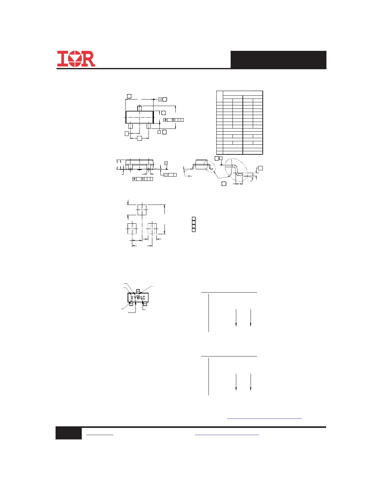
Micro3 (SOT-23 / TO-236AB) Part Marking Information
Micro3 (SOT-23) (Lead-Free) Package Outline
Dimensions are shown in millimeters (inches)
0.08
0.88
0.01
0.89
0.95 BSC
MILLIME TERS
MIN
e
E
E1
D
L
A
A1
A2
c
M
O
B
S
Y
MIN
MAX
MAX
.036
.0375 BSC
DIME NSIONS
INCHES
b
0.30
bbb
0.15
.008
ccc
.006
0.25 BS C
L1
L
0.40
0.60
.0118 BSC
aaa
0.20
.004
0°
8°
8°
0°
2.80
1.20
0
E1
E
D
5
6
3
1
2
ccc
C B A
B
5
6
e
e1
A2
A
A1
bbb
C A B
3X b
aaa C
3 S URF
0
3X L
L1
H
4
7
2.10
e1
1.90 BSC
.075 BSC
.0119
.0032
.111
.083
.048
.055
.119
.103
.0196
.0078
.0039
.044
.0004
.035
.040
.0236
.0158
1.02
0.20
0.50
2.64
3.04
1.40
1.12
0.10
0.10
1.90
[.075]
0.95
[.0375]
0.972
[.038]
2.742
[.1079]
0.802
[.031]
RECOMMENDED FOOTPRINT
3X
3X
NOT ES
1. DIMENSIONING AND T OLERANCING PER ASME Y14.5M-1994.
4 DATUM PLANE H IS LOCATED AT T HE MOLD PART ING LINE.
5 DATUM A AND B T O BE DET ERMINED AT DAT UM PLANE H.
6 DIMENSIONS D AND E1 ARE MEASURED AT DAT UM PLANE H.
2. DIMENSIONS ARE SHOWN IN MILLIMETERS AND INCHES.
3. CONT ROLLING DIMENSION: MILLIMET ER.
7 DIMENSION L IS T HE LEAD LENGTH FOR SOLDERING T O A SUBST RATE.
8. OUT LINE CONFORMS TO JEDEC OUT LINE T O-236AB.
F = IRLML6401
A
2001
A
27
Notes: This part marking information applies to devices produced after 02/26/2001
ASSEMBLY LOT CODE
LEAD-FREE
DATE CODE
E = IRLML6402
X = PART NUMBER CODE REFERENCE:
D = IRLML5103
C = IRLML6302
B = IRLML2803
A = IRLML2402
W = (1-26) IF PRECEDED BY LAST DIGIT OF CALENDAR YEAR
W = (27-52) IF PRECEDED BY A LETTER
Y
8
2008
3
2003
1
2001
YEAR
2002
2
5
2005
2004
4
2007
2006
7
6
2010
0
2009
9
YEAR
Y
C
03
WORK
WEEK
01
02
A
W
B
04
D
24
26
25
X
Z
Y
WORK
WEEK
W
H = IRLML5203
G = IRLML2502
K
H
G
F
E
D
C
B
2006
2003
2002
2005
2004
2008
2007
2010
2009
J
Y
51
29
28
30
C
B
D
50
X
I = IRLML0030
J = IRLML2030
L = IRLML0060
M = IRLML0040
K = IRLML0100
N = IRLML2060
P = IRLML9301
R = IRLML9303
Cu WIRE
HALOGEN FREE
PART NUMBER
52
Z
DATE CODE EXAMPLE:
YWW = 432 = DF
YWW = 503 = 5C
2018
2013
2011
2012
2015
2014
2017
2016
2020
2019
2018
2013
2011
2012
2015
2014
2017
2016
2020
2019
W = IRFML8244
V = IRLML6346
U = IRLML6344
T = IRLML6246
S = IRLML6244
Y = IRLML2246
X = IRLML2244
Z = IRFML9244
Note: For the most current drawing please refer to IR website at
http://www.irf.com/package
9
www.irf.com
©
2014 International Rectifier
Submit Datasheet Feedback
April 28, 2014
IRLML5203PbF
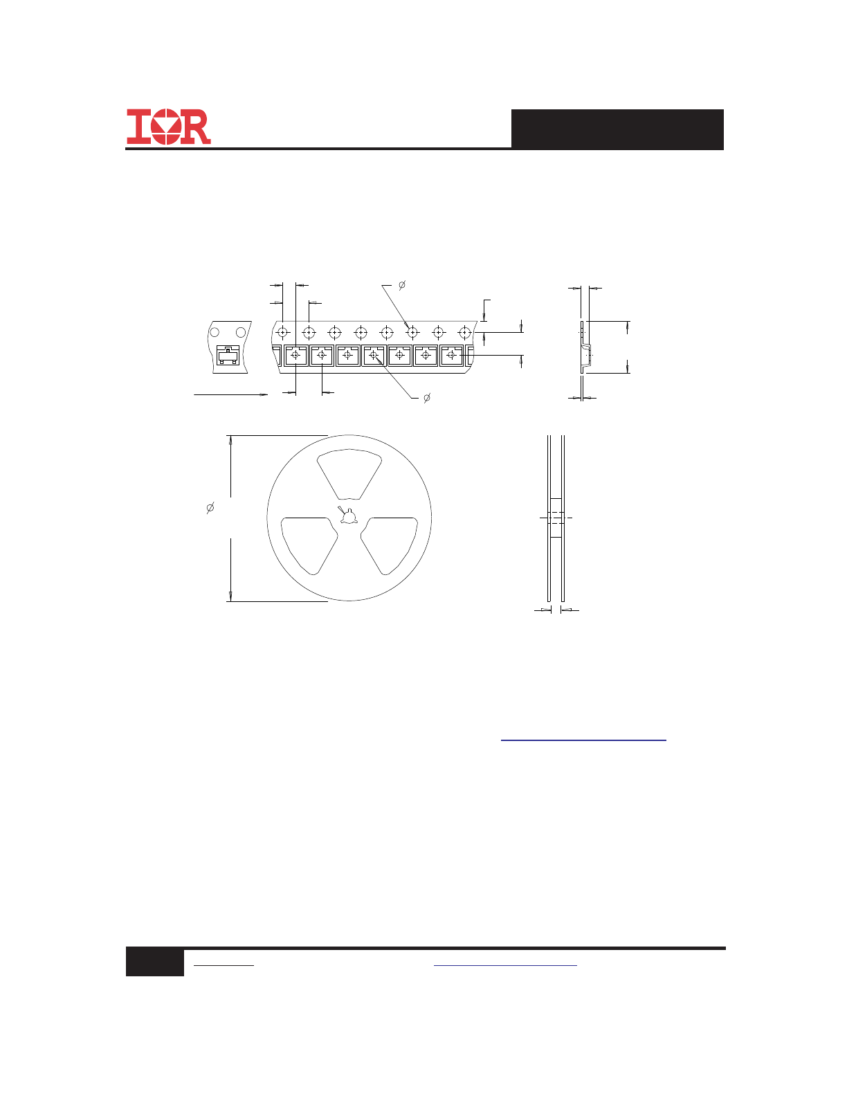
Micro3™ Tape & Reel Information
Dimensions are shown in millimeters (inches)
2.05 ( .080 )
1.95 ( .077 )
TR
FEED DIRECTION
4.1 ( .161 )
3.9 ( .154 )
1.6 ( .062 )
1.5 ( .060 )
1.85 ( .072 )
1.65 ( .065 )
3.55 ( .139 )
3.45 ( .136 )
1.1 ( .043 )
0.9 ( .036 )
4.1 ( .161 )
3.9 ( .154 )
0.35 ( .013 )
0.25 ( .010 )
8.3 ( .326 )
7.9 ( .312 )
1.32 ( .051 )
1.12 ( .045 )
9.90 ( .390 )
8.40 ( .331 )
178.00
( 7.008 )
MAX.
NOTES:
1. CONTROLLING DIMENSION : MILLIMETER.
2. OUTLINE CONFORMS TO EIA-481 & EIA-541.
Note: For the most current drawing please refer to IR website at
http://www.irf.com/package
10
www.irf.com
©
2014 International Rectifier
Submit Datasheet Feedback
April 28, 2014
IRLML5203PbF
MS L1
(per JEDEC J-S TD-020D
††
)
RoHS compliant
Yes
Qualification information
†
Qualification level
Consumer
(per JEDEC JES D47F
††
guidelines)
Moisture Sensitivity Level
Micro3
™ (SOT-23)
† Qualification standards can be found at International Rectifier’s web site:
http://www.irf.com/product-info/reliability
††
Applicable version of JEDEC standard at the time of product release
IR WORLD HEADQUARTERS: 101 N. Sepulveda Blvd., El Segundo, California 90245, USA
To contact International Rectifier, please visit
http://www.irf.com/whoto-call/
Revision History
Date
Comment
• Updated data sheet with new IR corporate template.
• Updated package outline & part marking on page 8.
• Added Qualification table -Qual level "Consumer" on page 10.
• Added bullet point in the Benefits "RoHS Compliant, Halogen -Free" on page 1.
4/28/2014