
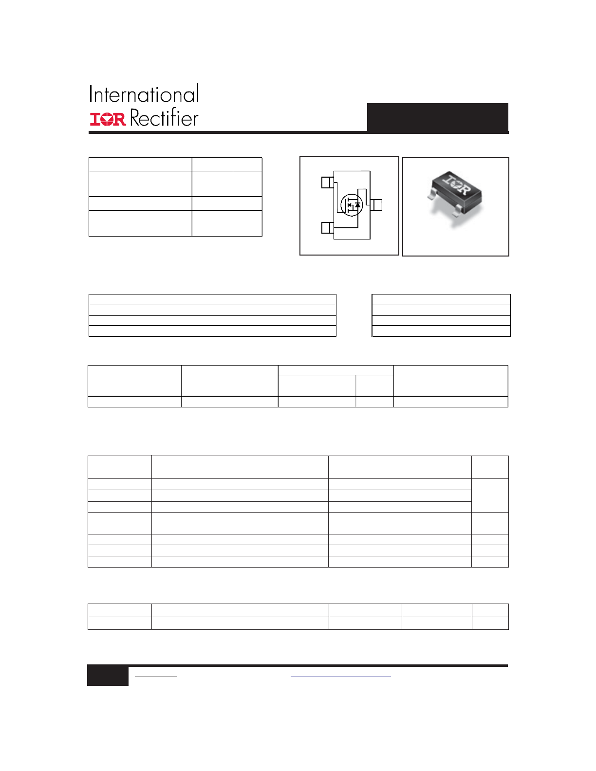
HEXFET
®
Power MOSFET
D
S
G
3
1
2
IRLML2502PbF-1
Features
Benefits
Industry-standard pinout SOT-23 Package
⇒
Multi-Vendor Compatibility
Compatible with Existing Surface Mount Techniques
Easier Manufacturing
RoHS Compliant, Halogen-Free
Environmentally Friendlier
MSL1, Industrial qualification
Increased Reliability
Micro3
™(SOT-23)
Form
Quantity
IRLML2502TRPbF-1
Micro3™ (SOT-23)
Tape and Reel
3000
IRLML2502TRPbF-1
Package Type
Standard Pack
Orderable Part Number
Base Part Number
Parameter
Max.
Units
V
DS
Drain- Source Voltage
20
V
I
D
@ T
A
= 25°C
Continuous Drain Current, V
GS
@ 4.5V
4.2
I
D
@ T
A
= 70°C
Continuous Drain Current, V
GS
@ 4.5V
3.4
A
I
DM
Pulsed Drain Current
33
P
D
@T
A
= 25°C
Power Dissipation
1.25
P
D
@T
A
= 70°C
Power Dissipation
0.8
Linear Derating Factor
0.01
W/°C
V
GS
Gate-to-Source Voltage
± 12
V
T
J,
T
STG
Junction and Storage Temperature Range
-55 to + 150
°C
Absolute Maximum Ratings
W
Parameter
Typ.
Max.
Units
R
θJA
Maximum Junction-to-Ambient
75
100
°C/W
Thermal Resistance
V
DS
20
V
R
DS(on) max
(@V
GS
= 4.5V)
0.045
Q
g (typical)
8.0
nC
I
D
(@T
A
= 25°C)
4.2
A
Ω
1
www.irf.com
©
2014 International Rectifier
Submit Datasheet Feedback
October 28, 2014
IRLML2502PbF-1
2
www.irf.com
©
2014 International Rectifier
Submit Datasheet Feedback
October 28, 2014
Repetitive rating; pulse width limited by
max. junction temperature. ( See fig. 11 )
Notes:
Pulse width ≤ 300μs; duty cycle ≤ 2%.
Surface mounted on FR-4 board, t ≤ 5sec.
S
D
G
Electrical Characteristics @ T
J
= 25°C (unless otherwise specified)
Parameter
Min.
Typ.
Max.
Units
V
(BR)DSS
Drain-to-Source Breakdown Voltage
20
–––
–––
V
ΔV
(BR)DSS
/
ΔT
J
Breakdown Voltage Temp. Coefficient
–––
0.01
–––
V/°C
R
DS(on)
Static Drain-to-Source On-Resistance
–––
0.035
0.045
Ω
–––
0.050
0.080
V
GS(th)
Gate Threshold Voltage
0.60
–––
1.2
V
ΔV
GS(th)
Gate Threshold Voltage Coefficient
–––
-3.2
–––
mV/°C
gfs
Forward Transconductance
5.8
–––
–––
S
I
DSS
Drain-to-Source Leakage Current
–––
–––
1.0
–––
–––
25
I
GSS
Gate-to-Source Forward Leakage
–––
–––
100
Gate-to-Source Reverse Leakage
–––
–––
-100
Q
g
Total Gate Charge
–––
8.0
12
Q
gs
Gate-to-Source Charge
–––
1.8
2.7
Q
gd
Gate-to-Drain ("Miller") Charge
–––
1.7
2.6
t
d(on)
Turn-On Delay Time
–––
7.5
–––
t
r
Rise Time
–––
10
–––
t
d(off)
Turn-Off Delay Time
–––
54
–––
t
f
Fall Time
–––
26
–––
C
iss
Input Capacitance
–––
740
–––
C
oss
Output Capacitance
–––
90
–––
C
rss
Reverse Transfer Capacitance
–––
66
–––
Source-Drain Rating and Characteristics
Parameter
Min.
Typ.
Max.
Units
I
S
Continuous Source Current
(Body Diode)
I
SM
Pulsed Source Current
(Body Diode)c
V
SD
Diode Forward Voltage
–––
–––
1.2
V
t
rr
Reverse Recovery Time
–––
16
24
ns
Q
rr
Reverse Recovery Charge
–––
8.6
13
nC
MOSFET symbol
nA
ns
A
pF
nC
V
DS
= 10V
V
GS
= 12V
V
GS
= -12V
Conditions
V
GS
= 0V, I
D
= 250uA
Reference to 25°C, I
D
= 1.0mA
V
GS
= 4.5V, I
D
= 4.2A d
–––
–––
33
–––
–––
1.3
Conditions
R
D
= 10
Ω d
ƒ = 1.0MHz
T
J
= 25°C, I
F
= 1.3A
di/dt = 100A/μs d
T
J
= 25°C, I
S
= 1.3A, V
GS
= 0V d
showing the
integral reverse
p-n junction diode.
R
G
= 6
Ω
V
DS
= 10V, I
D
= 4.0A
V
DS
= 16V, V
GS
= 0V, T
J
= 70°C
μA
V
GS
= 5.0V d
I
D
= 1.0A
V
GS
= 0V
V
DS
= 15V
I
D
= 4.0A
V
DS
= V
GS
, I
D
= 250μA
V
GS
= 2.5V, I
D
= 3.6A d
V
DS
= 16V, V
GS
= 0V
V
DD
= 10V
IRLML2502PbF-1
3
www.irf.com
©
2014 International Rectifier
Submit Datasheet Feedback
October 28, 2014
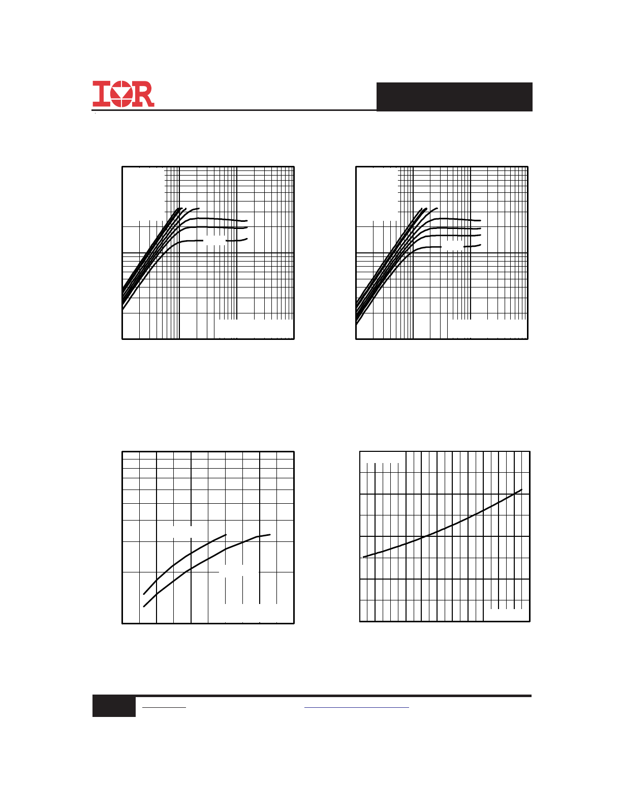
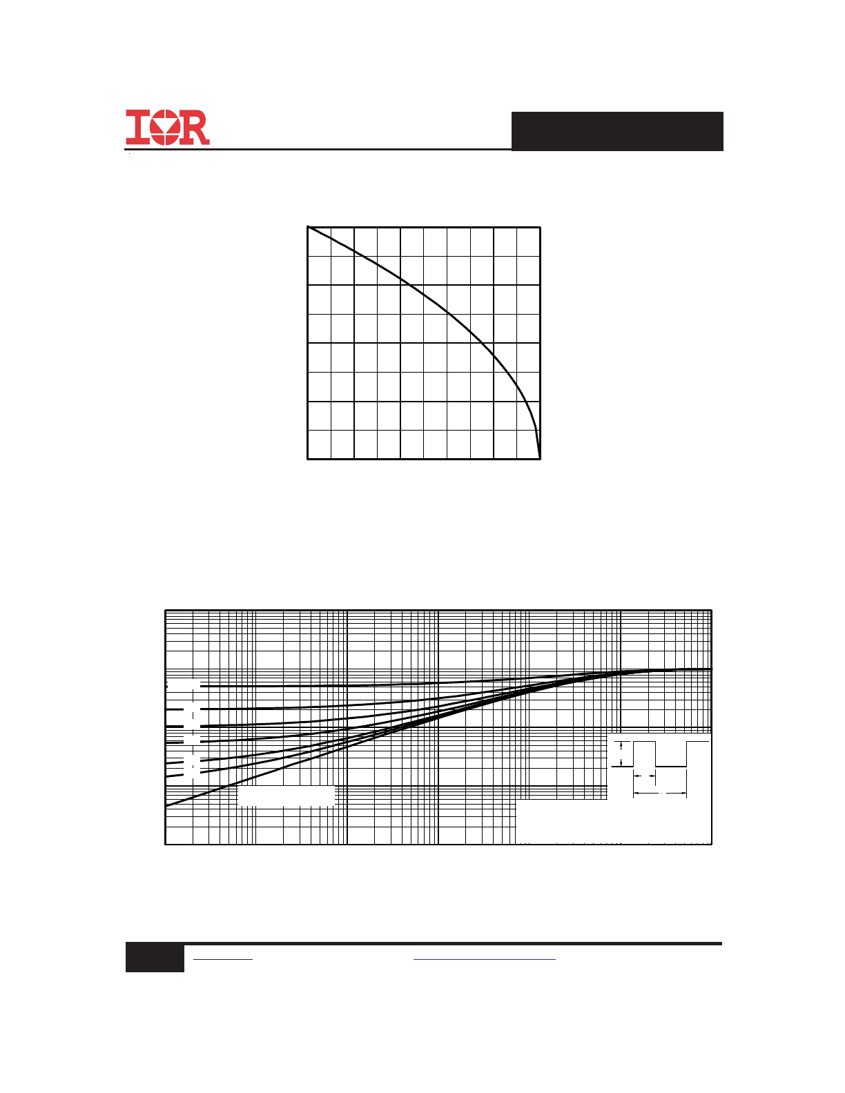
Fig 4. Normalized On-Resistance
Vs. Temperature
Fig 2. Typical Output Characteristics
Fig 1. Typical Output Characteristics
Fig 3. Typical Transfer Characteristics
-60 -40 -20
0
20 40 60 80 100 120 140 160
0.0
0.5
1.0
1.5
2.0
T , Junction Temperature ( C)
R , Drain-to-Source On Resistance
(Normalized)
J
D
S
(on)
°
V
=
I =
GS
D
4.5V
4.0A
1
10
100
0.1
1
10
100
20μs PULSE WIDTH
T = 25 C
J
°
TOP
BOTTOM
VGS
7.00V
5.00V
4.50V
3.50V
3.00V
2.70V
2.50V
2.25V
V , Drain-to-Source Voltage (V)
I , D
rain-to-S
ource C
urrent (A
)
DS
D
2.25V
1
10
100
0.1
1
10
100
20μs PULSE WIDTH
T = 150 C
J
°
TOP
BOTTOM
VGS
7.00V
5.00V
4.50V
3.50V
3.00V
2.70V
2.50V
2.25V
V , Drain-to-Source Voltage (V)
I , D
rain-to-S
ource C
urrent (A
)
DS
D
2.25V
10
100
2.0
2.4
2.8
3.2
3.6
4.0
V = 15V
20μs PULSE WIDTH
DS
V , Gate-to-Source Voltage (V)
I , D
rain-to-S
ource C
urrent (A
)
GS
D
T = 25 C
J
°
T = 150 C
J
°
IRLML2502PbF-1
4
www.irf.com
©
2014 International Rectifier
Submit Datasheet Feedback
October 28, 2014
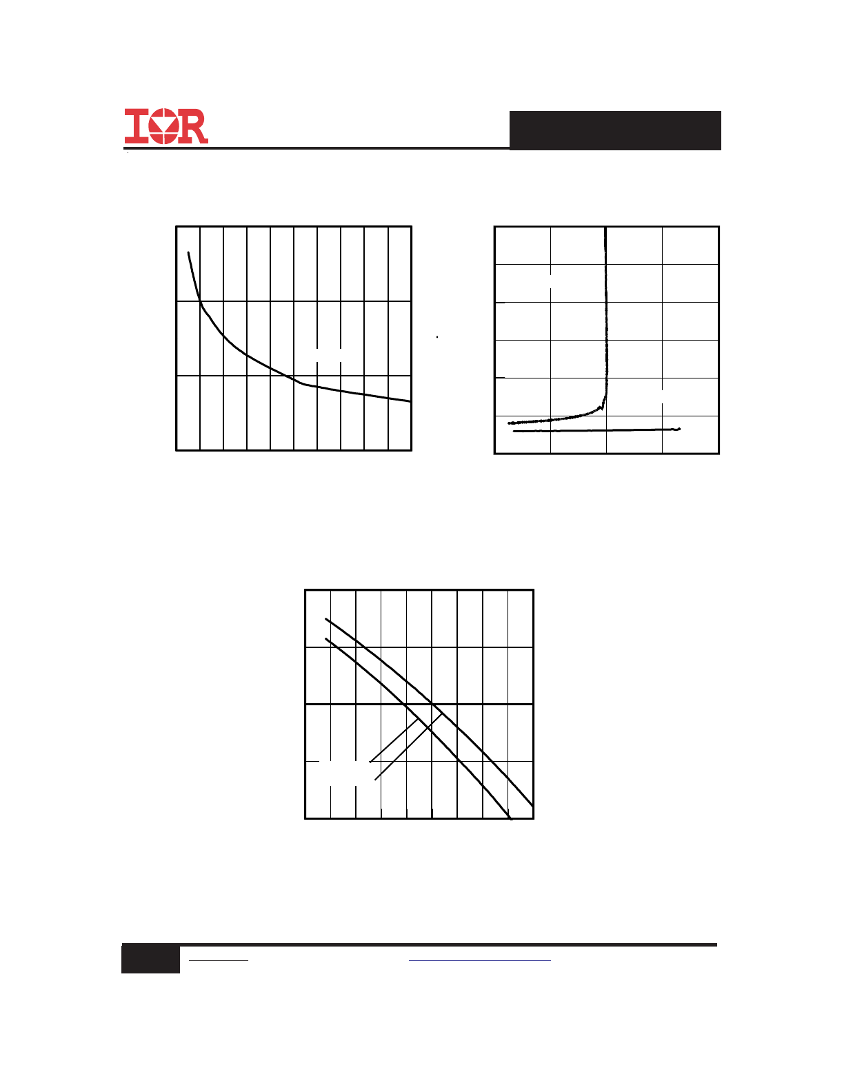
Fig 8. Maximum Safe Operating Area
Fig 6. Typical Gate Charge Vs.
Gate-to-Source Voltage
Fig 5. Typical Capacitance Vs.
Drain-to-Source Voltage
Fig 7. Typical Source-Drain Diode
Forward Voltage
0
4
8
12
16
0
2
4
6
8
10
Q , Total Gate Charge (nC)
V , Gate-to-Source Voltage (V)
G
GS
I =
D
4.0A
V
= 10V
DS
0.1
1
10
100
0.4
0.6
0.8
1.0
1.2
1.4
V ,Source-to-Drain Voltage (V)
I , Reverse Drain Current (A)
SD
SD
V = 0 V
GS
T = 25 C
J
°
T = 150 C
J
°
0.1
1
10
100
1000
0.1
1
10
100
OPERATION IN THIS AREA LIMITED
BY R
DS(on)
Single Pulse
T
T
= 150 C
= 25 C
°
°
J
A
V , Drain-to-Source Voltage (V)
I , Drain Current (A)I , Drain Current (A)
DS
D
10us
100us
1ms
10ms
1
10
100
0
200
400
600
800
1000
1200
V , Drain-to-Source Voltage (V)
C, Capacitance (pF)
DS
V
C
C
C
=
=
=
=
0V,
C
C
C
f = 1MHz
+ C
+ C
C SHORTED
GS
iss
gs
gd ,
ds
rss
gd
oss
ds
gd
C
rss
C
oss
C
iss
IRLML2502PbF-1
5
www.irf.com
©
2014 International Rectifier
Submit Datasheet Feedback
October 28, 2014
Fig 10. Maximum Effective Transient Thermal Impedance, Junction-to-Ambient
Fig 9. Maximum Drain Current Vs.
Case Temperature
25
50
75
100
125
150
0.0
1.0
2.0
3.0
4.0
T , Case Temperature ( C)
I , Drain Current (A)
°
C
D
0.1
1
10
100
1000
0.00001
0.0001
0.001
0.01
0.1
1
10
Notes:
1. Duty factor D = t / t
2. Peak T = P
x Z
+ T
1
2
J
DM
thJA
A
P
t
t
DM
1
2
t , Rectangular Pulse Duration (sec)
Ther
m
al
R
esponse
(Z
)
1
th
JA
0.01
0.02
0.05
0.10
0.20
D = 0.50
SINGLE PULSE
(THERMAL RESPONSE)
IRLML2502PbF-1
6
www.irf.com
©
2014 International Rectifier
Submit Datasheet Feedback
October 28, 2014
Fig 12. On-Resistance Vs. Drain Current
Fig 11. On-Resistance Vs. Gate Voltage
2.0 2.5 3.0 3.5 4.0 4.5 5.0 5.5 6.0 6.5 7.0
VGS, Gate -to -Source Voltage ( V )
0.02
0.03
0.04
0.05
R
D
S
(o
n)
,
D
ra
in
-t
o
-S
ou
rc
e
V
ol
ta
ge
(
Ω
)
Id = 4.0A
0
10
20
30
40
iD , Drain Current ( A )
0.00
0.10
0.20
0.30
R
D
S
(
o
n
)
, D
ra
in
-t
o-
S
ou
rc
e
O
n
R
es
is
ta
nc
e
( Ω
)
VGS = 4.5V
VGS = 2.5V
-75 -50 -25
0
25
50
75 100 125 150
TJ , Temperature ( °C )
0.5
0.7
0.9
1.1
1.3
V
G
S
(t
h)
,
G
at
e
th
re
sh
ol
d
V
ol
ta
ge
(
V
)
ID = 50μA
ID = 250μA
Fig 13. Threshold Voltage Vs. Temperature
IRLML2502PbF-1
7
www.irf.com
©
2014 International Rectifier
Submit Datasheet Feedback
October 28, 2014
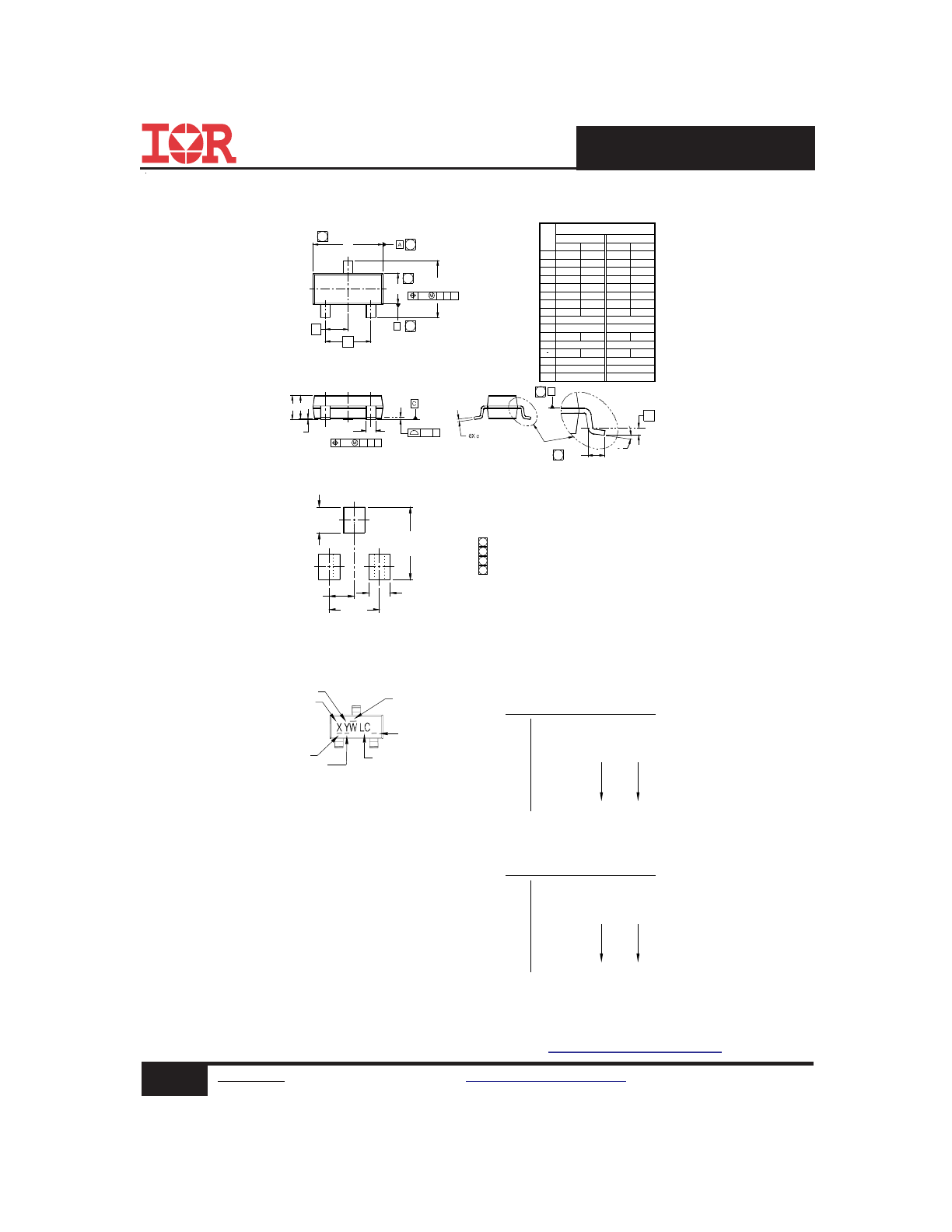
Micro3 (SOT-23 / TO-236AB) Part Marking Information
Micro3 (SOT-23) (Lead-Free) Package Outline
Dimensions are shown in millimeters (inches)
0.08
0.88
0.01
0.89
0.95 BSC
MILLIME TERS
MIN
e
E
E1
D
L
A
A1
A2
c
M
O
B
S
Y
MIN
MAX
MAX
.036
.0375 BSC
DIME NSIONS
INCHES
b
0.30
bbb
0.15
.008
ccc
.006
0.25 BS C
L1
L
0.40
0.60
.0118 BSC
aaa
0.20
.004
0°
8°
8°
0°
2.80
1.20
0
E1
E
D
5
6
3
1
2
ccc
C B A
B
5
6
e
e1
A2
A
A1
bbb
C A B
3X b
aaa C
3 S URF
0
3X L
L1
H
4
7
2.10
e1
1.90 BSC
.075 BSC
.0119
.0032
.111
.083
.048
.055
.119
.103
.0196
.0078
.0039
.044
.0004
.035
.040
.0236
.0158
1.02
0.20
0.50
2.64
3.04
1.40
1.12
0.10
0.10
1.90
[.075]
0.95
[.0375]
0.972
[.038]
2.742
[.1079]
0.802
[.031]
RECOMMENDED FOOTPRINT
3X
3X
NOT ES
1. DIMENSIONING AND T OLERANCING PER ASME Y14.5M-1994.
4 DATUM PLANE H IS LOCATED AT T HE MOLD PART ING LINE.
5 DATUM A AND B T O BE DET ERMINED AT DAT UM PLANE H.
6 DIMENSIONS D AND E1 ARE MEASURED AT DAT UM PLANE H.
2. DIMENSIONS ARE SHOWN IN MILLIMETERS AND INCHES.
3. CONT ROLLING DIMENSION: MILLIMET ER.
7 DIMENSION L IS T HE LEAD LENGTH FOR SOLDERING T O A SUBST RATE.
8. OUT LINE CONFORMS TO JEDEC OUT LINE T O-236AB.
Note: For the most current drawing please refer to IR website at
http://www.irf.com/package/
F = IRLML6401
A
A
27
LOT CODE
LEAD FREE
DATE CODE
E = IRLML6402
X = PART NUMBER CODE REFERENCE:
D = IRLML5103
C = IRLML6302
B = IRLML2803
A = IRLML2402
W = (1-26) IF PRECEDED BY LAST DIGIT OF CALENDAR YEAR
W = (27-52) IF PRECEDED BY A LETTER
Y
8
3
1
2
5
4
7
6
0
9
Y
C
03
WORK
WEEK
01
02
A
W
B
04
D
24
26
25
X
Z
Y
WORK
WEEK
W
H = IRLML5203
G = IRLML2502
K
H
G
F
E
D
C
B
J
Y
51
29
28
30
C
B
D
50
X
52
Z
Note: A line above the work week
(as shown here) indicates Lead - Free.
I = IRLML0030
J = IRLML2030
L = IRLML0060
M = IRLML0040
K = IRLML0100
N = IRLML2060
P = IRLML9301
R = IRLML9303
Cu WIRE
HALOGEN FREE
PART NUMBER
X = IRLML2244
W = IRFML8244
V = IRLML6346
U = IRLML6344
T = IRLML6246
S = IRLML6244
Z = IRFML9244
Y = IRLML2246
INDUSTRIAL VERSION
2007
YEAR
2003
2001
2002
2005
2004
2006
2007
2009
2008
2010
2003
2001
YEAR
2002
2005
2004
2006
2009
2008
2010
2017
2013
2011
2012
2015
2014
2016
2017
2019
2018
2020
2013
2011
2012
2015
2014
2016
2019
2018
2020
IRLML2502PbF-1
8
www.irf.com
©
2014 International Rectifier
Submit Datasheet Feedback
October 28, 2014
Micro3™ Tape & Reel Information
(Dimensions are shown in millimeters (inches))
2.05 ( .080 )
1.95 ( .077 )
TR
FEED DIRECTION
4.1 ( .161 )
3.9 ( .154 )
1.6 ( .062 )
1.5 ( .060 )
1.85 ( .072 )
1.65 ( .065 )
3.55 ( .139 )
3.45 ( .136 )
1.1 ( .043 )
0.9 ( .036 )
4.1 ( .161 )
3.9 ( .154 )
0.35 ( .013 )
0.25 ( .010 )
8.3 ( .326 )
7.9 ( .312 )
1.32 ( .051 )
1.12 ( .045 )
9.90 ( .390 )
8.40 ( .331 )
178.00
( 7.008 )
MAX.
NOTES:
1. CONTROLLING DIMENSION : MILLIMETER.
2. OUTLINE CONFORMS TO EIA-481 & EIA-541.
Note: For the most current drawing please refer to IR website at
: http://www.irf.com/package/
† Qualification standards can be found at International Rectifier’s web site:
http://www.irf.com/product-info/reliability
††
Applicable version of JEDEC standard at the time of product release
IR WORLD HEADQUARTERS: 101 N. Sepulveda Blvd., El Segundo, California 90245, USA
To contact International Rectifier, please visit
http://www.irf.com/whoto-call/
MS L1
(per JEDEC J-S TD-020D
††
)
RoHS compliant
Yes
Qualification information
†
Qualification level
Industrial
(per JEDEC JES D47F
††
guidelines)
Moisture Sensitivity Level
Micro3
™ (SOT-23)
Revision History
Date
Comment
10/28/2014
• Updated partmarking to reflect Industrial partmarking on page 7.