
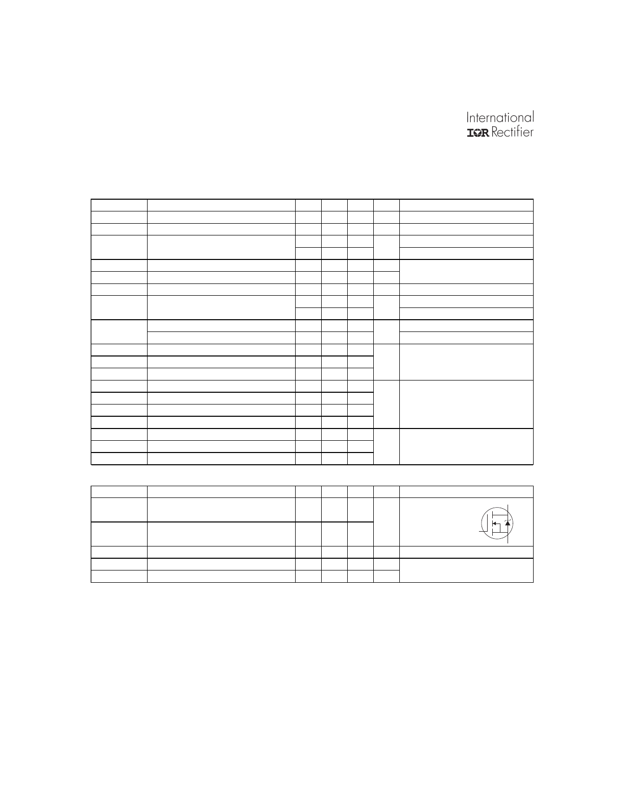
Parameter
Typ.
Max.
Units
R
θJA
Maximum Junction-to-Ambient
75
100
°C/W
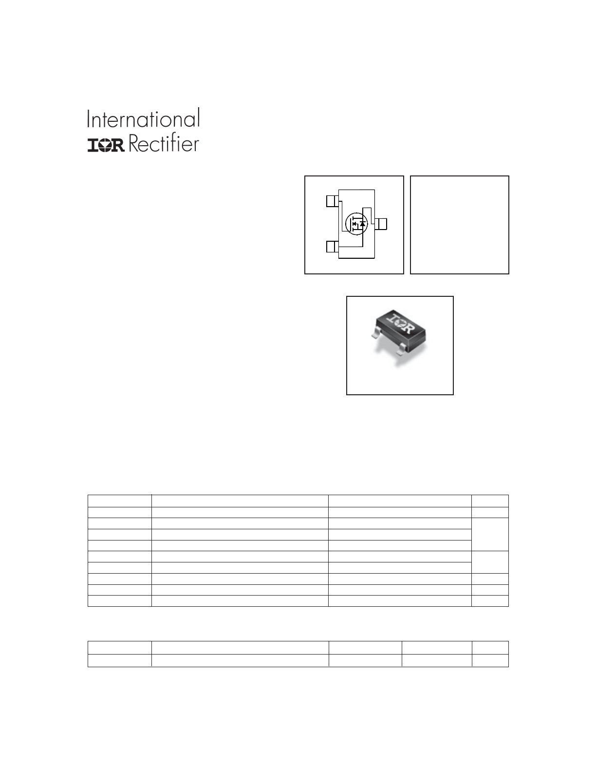
IRLML2502GPbF
HEXFET
®
Power MOSFET
These N-Channel MOSFETs from International Rectifier
utilize advanced processing techniques to achieve extremely
low on-resistance per silicon area. This benefit, combined
with the fast switching speed and ruggedized device design
that HEXFET
®
power MOSFETs are well known for, provides
the designer with an extremely efficient and reliable device
for use in battery and load management.
A thermally enhanced large pad leadframe has been
incorporated into the standard SOT-23 package to produce
a HEXFET Power MOSFET with the industry's smallest
footprint. This package, dubbed the Micro3
™, is ideal for
applications where printed circuit board space is at a
premium. The low profile (<1.1mm) of the Micro3 allows it
to fit easily into extremely thin application environments
such as portable electronics and PCMCIA cards. The thermal
resistance and power dissipation are the best available.
Thermal Resistance
V
DSS
= 20V
R
DS(on)
= 0.045
Ω
l
Ultra Low On-Resistance
l
N-Channel MOSFET
l
SOT-23 Footprint
l
Low Profile (<1.1mm)
l
Available in Tape and Reel
l
Fast Switching
l
Lead-Free
l
Halogen-Free
Description
09/25/12
www.irf.com
1
Parameter
Max.
Units
V
DS
Drain- Source Voltage
20
V
I
D
@ T
A
= 25°C
Continuous Drain Current, V
GS
@ 4.5V
4.2
I
D
@ T
A
= 70°C
Continuous Drain Current, V
GS
@ 4.5V
3.4
A
I
DM
Pulsed Drain Current
33
P
D
@T
A
= 25°C
Power Dissipation
1.25
P
D
@T
A
= 70°C
Power Dissipation
0.8
Linear Derating Factor
0.01
W/°C
V
GS
Gate-to-Source Voltage
± 12
V
T
J,
T
STG
Junction and Storage Temperature Range
-55 to + 150
°C
Absolute Maximum Ratings
W
Micro3
™
D
S
G
3
1
2
PD - 96163A
IRLML2502GPbF
2
www.irf.com
Repetitive rating; pulse width limited by
max. junction temperature. ( See fig. 11 )
Notes:
Pulse width ≤ 300μs; duty cycle ≤ 2%.
Surface mounted on FR-4 board, t ≤ 5sec.
S
D
G
Electrical Characteristics @ T
J
= 25°C (unless otherwise specified)
Parameter
Min.
Typ.
Max.
Units
V
(BR)DSS
Drain-to-Source Breakdown Voltage
20
–––
–––
V
ΔV
(BR)DSS
/
ΔT
J
Breakdown Voltage Temp. Coefficient
–––
0.01
–––
V/°C
R
DS(on)
Static Drain-to-Source On-Resistance
–––
0.035
0.045
Ω
–––
0.050
0.080
V
GS(th)
Gate Threshold Voltage
0.60
–––
1.2
V
ΔV
GS(th)
Gate Threshold Voltage Coefficient
–––
-3.2
–––
mV/°C
gfs
Forward Transconductance
5.8
–––
–––
S
I
DSS
Drain-to-Source Leakage Current
–––
–––
1.0
–––
–––
25
I
GSS
Gate-to-Source Forward Leakage
–––
–––
100
Gate-to-Source Reverse Leakage
–––
–––
-100
Q
g
Total Gate Charge
–––
8.0
12
Q
gs
Gate-to-Source Charge
–––
1.8
2.7
Q
gd
Gate-to-Drain ("Miller") Charge
–––
1.7
2.6
t
d(on)
Turn-On Delay Time
–––
7.5
–––
t
r
Rise Time
–––
10
–––
t
d(off)
Turn-Off Delay Time
–––
54
–––
t
f
Fall Time
–––
26
–––
C
iss
Input Capacitance
–––
740
–––
C
oss
Output Capacitance
–––
90
–––
C
rss
Reverse Transfer Capacitance
–––
66
–––
Source-Drain Rating and Characteristics
Parameter
Min.
Typ.
Max.
Units
I
S
Continuous Source Current
(Body Diode)
I
SM
Pulsed Source Current
(Body Diode)c
V
SD
Diode Forward Voltage
–––
–––
1.2
V
t
rr
Reverse Recovery Time
–––
16
24
ns
Q
rr
Reverse Recovery Charge
–––
8.6
13
nC
MOSFET symbol
nA
ns
A
pF
nC
V
DS
= 10V
V
GS
= 12V
V
GS
= -12V
Conditions
V
GS
= 0V, I
D
= 250uA
Reference to 25°C, I
D
= 1.0mA
V
GS
= 4.5V, I
D
= 4.2A d
–––
–––
33
–––
–––
1.3
Conditions
R
D
= 10
Ω
d
ƒ = 1.0MHz
T
J
= 25°C, I
F
= 1.3A
di/dt = 100A/μs d
T
J
= 25°C, I
S
= 1.3A, V
GS
= 0V d
showing the
integral reverse
p-n junction diode.
R
G
= 6
Ω
V
DS
= 10V, I
D
= 4.0A
V
DS
= 16V, V
GS
= 0V, T
J
= 70°C
μA
V
GS
= 5.0V d
I
D
= 1.0A
V
GS
= 0V
V
DS
= 15V
I
D
= 4.0A
V
DS
= V
GS
, I
D
= 250μA
V
GS
= 2.5V, I
D
= 3.6A d
V
DS
= 16V, V
GS
= 0V
V
DD
= 10V
IRLML2502GPbF
www.irf.com
3
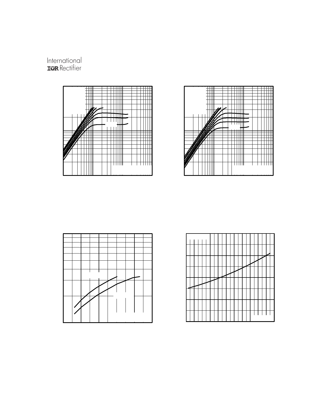
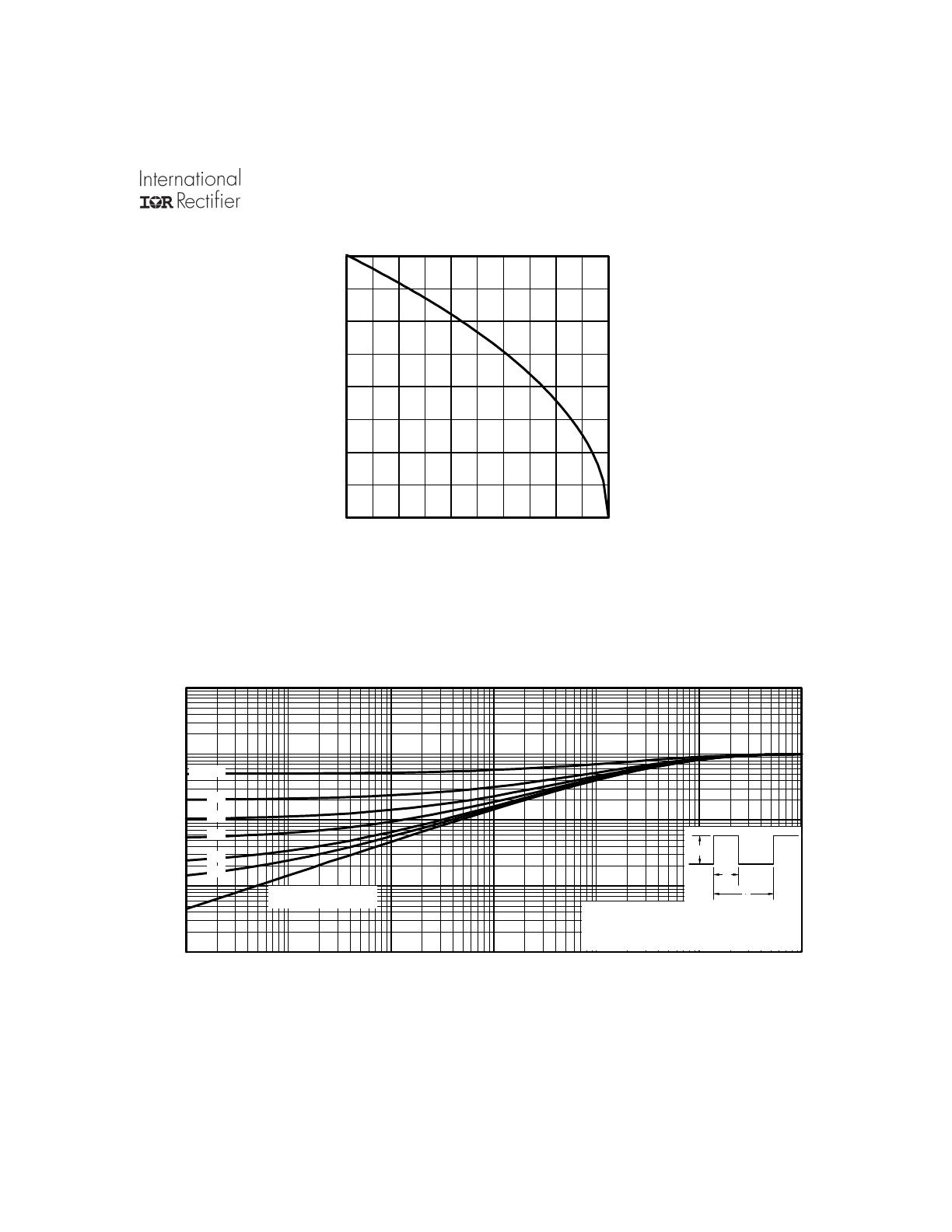
Fig 4. Normalized On-Resistance
Vs. Temperature
Fig 2. Typical Output Characteristics
Fig 1. Typical Output Characteristics
Fig 3. Typical Transfer Characteristics
-60 -40 -20
0
20 40 60 80 100 120 140 160
0.0
0.5
1.0
1.5
2.0
T , Junction Temperature ( C)
R , Drain-to-Source On Resistance
(Normalized)
J
D
S
(on)
°
V
=
I =
GS
D
4.5V
4.0A
1
10
100
0.1
1
10
100
20μs PULSE WIDTH
T = 25 C
J
°
TOP
BOTTOM
VGS
7.00V
5.00V
4.50V
3.50V
3.00V
2.70V
2.50V
2.25V
V , Drain-to-Source Voltage (V)
I , D
rain-to-S
ource C
urrent (A
)
DS
D
2.25V
1
10
100
0.1
1
10
100
20μs PULSE WIDTH
T = 150 C
J
°
TOP
BOTTOM
VGS
7.00V
5.00V
4.50V
3.50V
3.00V
2.70V
2.50V
2.25V
V , Drain-to-Source Voltage (V)
I , D
rain-to-S
ource C
urrent (A
)
DS
D
2.25V
10
100
2.0
2.4
2.8
3.2
3.6
4.0
V = 15V
20μs PULSE WIDTH
DS
V , Gate-to-Source Voltage (V)
I , D
rain-to-S
ource C
urrent (A
)
GS
D
T = 25 C
J
°
T = 150 C
J
°
IRLML2502GPbF
4
www.irf.com
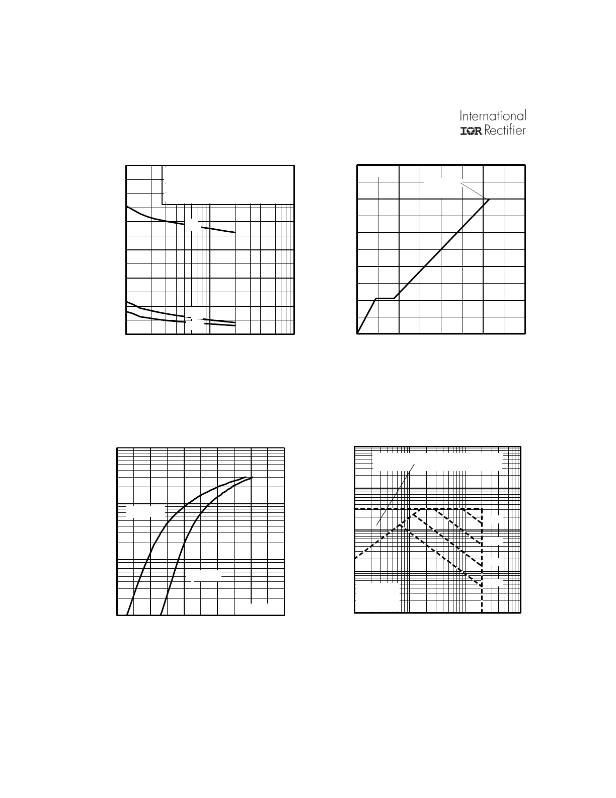
Fig 8. Maximum Safe Operating Area
Fig 6. Typical Gate Charge Vs.
Gate-to-Source Voltage
Fig 5. Typical Capacitance Vs.
Drain-to-Source Voltage
Fig 7. Typical Source-Drain Diode
Forward Voltage
0
4
8
12
16
0
2
4
6
8
10
Q , Total Gate Charge (nC)
V , Gate-to-Source Voltage (V)
G
GS
I =
D
4.0A
V
= 10V
DS
0.1
1
10
100
0.4
0.6
0.8
1.0
1.2
1.4
V ,Source-to-Drain Voltage (V)
I , Reverse Drain Current (A)
SD
SD
V = 0 V
GS
T = 25 C
J
°
T = 150 C
J
°
0.1
1
10
100
1000
0.1
1
10
100
OPERATION IN THIS AREA LIMITED
BY R
DS(on)
Single Pulse
T
T
= 150 C
= 25 C
°
°
J
A
V , Drain-to-Source Voltage (V)
I , Drain Current (A)I , Drain Current (A)
DS
D
10us
100us
1ms
10ms
1
10
100
0
200
400
600
800
1000
1200
V , Drain-to-Source Voltage (V)
C, Capacitance (pF)
DS
V
C
C
C
=
=
=
=
0V,
C
C
C
f = 1MHz
+ C
+ C
C SHORTED
GS
iss
gs
gd ,
ds
rss
gd
oss
ds
gd
C
rss
C
oss
C
iss
IRLML2502GPbF
www.irf.com
5
Fig 10. Maximum Effective Transient Thermal Impedance, Junction-to-Ambient
Fig 9. Maximum Drain Current Vs.
Case Temperature
25
50
75
100
125
150
0.0
1.0
2.0
3.0
4.0
T , Case Temperature ( C)
I , Drain Current (A)
°
C
D
0.1
1
10
100
1000
0.00001
0.0001
0.001
0.01
0.1
1
10
Notes:
1. Duty factor D = t / t
2. Peak T = P
x Z
+ T
1
2
J
DM
thJA
A
P
t
t
DM
1
2
t , Rectangular Pulse Duration (sec)
Ther
m
al
R
esponse
(Z
)
1
th
JA
0.01
0.02
0.05
0.10
0.20
D = 0.50
SINGLE PULSE
(THERMAL RESPONSE)
IRLML2502GPbF
6
www.irf.com
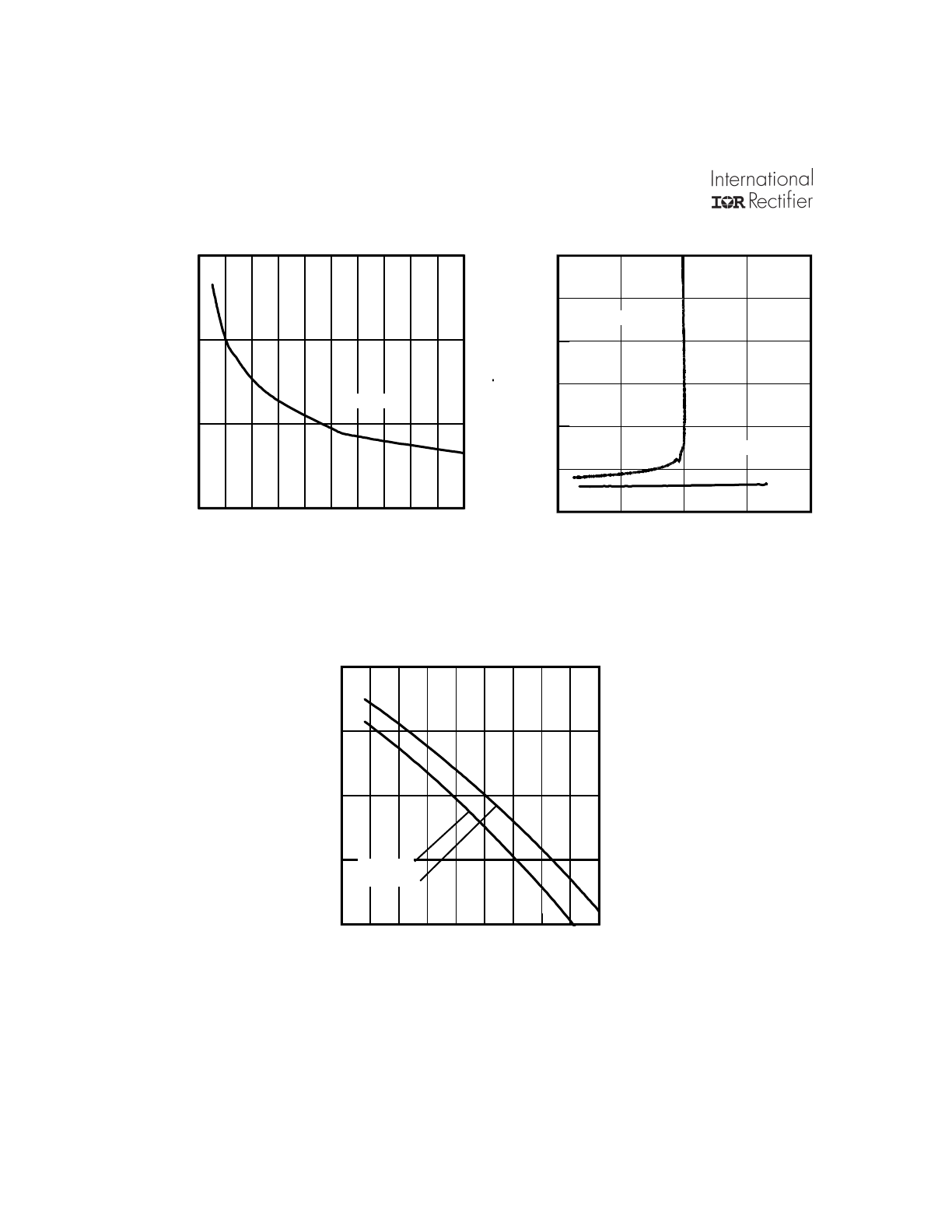
Fig 12. On-Resistance Vs. Drain Current
Fig 11. On-Resistance Vs. Gate Voltage
2.0 2.5 3.0 3.5 4.0 4.5 5.0 5.5 6.0 6.5 7.0
VGS, Gate -to -Source Voltage ( V )
0.02
0.03
0.04
0.05
R
D
S
(o
n)
,
D
ra
in
-t
o
-S
ou
rc
e
V
ol
ta
ge
(
Ω
)
Id = 4.0A
0
10
20
30
40
iD , Drain Current ( A )
0.00
0.10
0.20
0.30
R
D
S
(
o
n
)
, D
ra
in
-t
o-
S
ou
rc
e
O
n
R
es
is
ta
nc
e
( Ω
)
VGS = 4.5V
VGS = 2.5V
-75 -50 -25
0
25
50
75 100 125 150
TJ , Temperature ( °C )
0.5
0.7
0.9
1.1
1.3
V
G
S
(t
h)
,
G
at
e
th
re
sh
ol
d
V
ol
ta
ge
(
V
)
ID = 50μA
ID = 250μA
Fig 13. Threshold Voltage Vs. Temperature
IRLML2502GPbF
www.irf.com
7
Micro3 (SOT-23/TO-236AB) Part Marking Information
Micro3 (SOT-23) Package Outline
Dimensions are shown in millimeters (inches)
Note: For the most current drawing please refer to IR website at: http://www.irf.com/package/
e
E1
E
D
A
B
0.15 [0.006]
e1
1
2
3
M C B A
5
6
6
5
NOTES:
b
A1
3X
A
A2
A
B
C
M
0.20 [0.008]
0.10 [0.004] C
C
1. DIMENSIONING & TOLERANCING PER ANSI Y14.5M-1994
2. DIMENSIONS ARE SHOWN IN MILLIMETERS [INCHES].
3. CONTROLLING DIMENSION: MILLIMETER.
4. DATUM PLANE H IS LOCATED AT THE MOLD PARTING LINE.
5. DATUM A AND B TO BE DETERMINED AT DATUM PLANE H.
6. DIMENSIONS D AND E1 ARE MEASURED AT DATUM PLANE H. DIMENSIONS DOES
NOT INCLUDE MOLD PROTRUSIONS OR INTERLEAD FLASH. MOLD PROTRUSIONS
OR INTERLEAD FLASH SHALL NOT EXCEED 0.25 MM [0.010 INCH] PER SIDE.
7. DIMENSION L IS THE LEAD LENGTH FOR SOLDERING TO A SUBSTRATE.
8. OUTLINE CONFORMS TO JEDEC OUTLINE TO-236 AB.
0.89
1.12
SYMBOL
MAX
MIN
A1
b
0.01
0.10
c
0.30
0.50
D
0.08
0.20
E
2.80
3.04
E1
2.10
2.64
e
1.20
1.40
A
0.95
BSC
L
0.40
0.60
0
8
MILLIMETERS
A2
0.88
1.02
e1
1.90
BSC
REF
0.54
L1
BSC
0.25
L2
BSC
REF
%6&
INCHES
8
0
%6&
0.0004
MIN
MAX
DIMENSIONS
0.972
1.900
Recommended Footprint
0.802
0.950
2.742
3X L
c
L2
H 4
L1
7
F = IRLML6401
A
2001
A
27
Notes: This part marking information applies to devices produced after 02/26/2001
LOT CODE
LEAD FREE
DATE CODE
E = IRLML6402
X = PART NUMBER CODE REFERENCE:
D = IRLML5103
C = IRLML6302
B = IRLML2803
A = IRLML2402
W = (1-26) IF PRECEDED BY LAST DIGIT OF CALENDAR YEAR
W = (27-52) IF PRECEDED BY A LETTER
Y
8
2008
3
2003
1
2001
YEAR
2002
2
5
2005
2004
4
2007
2006
7
6
2010
0
2009
9
YEAR
Y
C
03
WORK
WEEK
01
02
A
W
B
04
D
24
26
25
X
Z
Y
WORK
WEEK
W
H = IRLML5203
G = IRLML2502
K
H
G
F
E
D
C
B
2006
2003
2002
2005
2004
2008
2007
2010
2009
J
29
28
30
C
B
D
50
X
I = IRLML0030
J = IRLML2030
L = IRLML0060
M = IRLML0040
K = IRLML0100
N = IRLML2060
P = IRLML9301
R = IRLML9303
Cu WIRE
HALOGEN FREE
PART NUMBER
IRLML2502GPbF
8
www.irf.com
Data and specifications subject to change without notice.
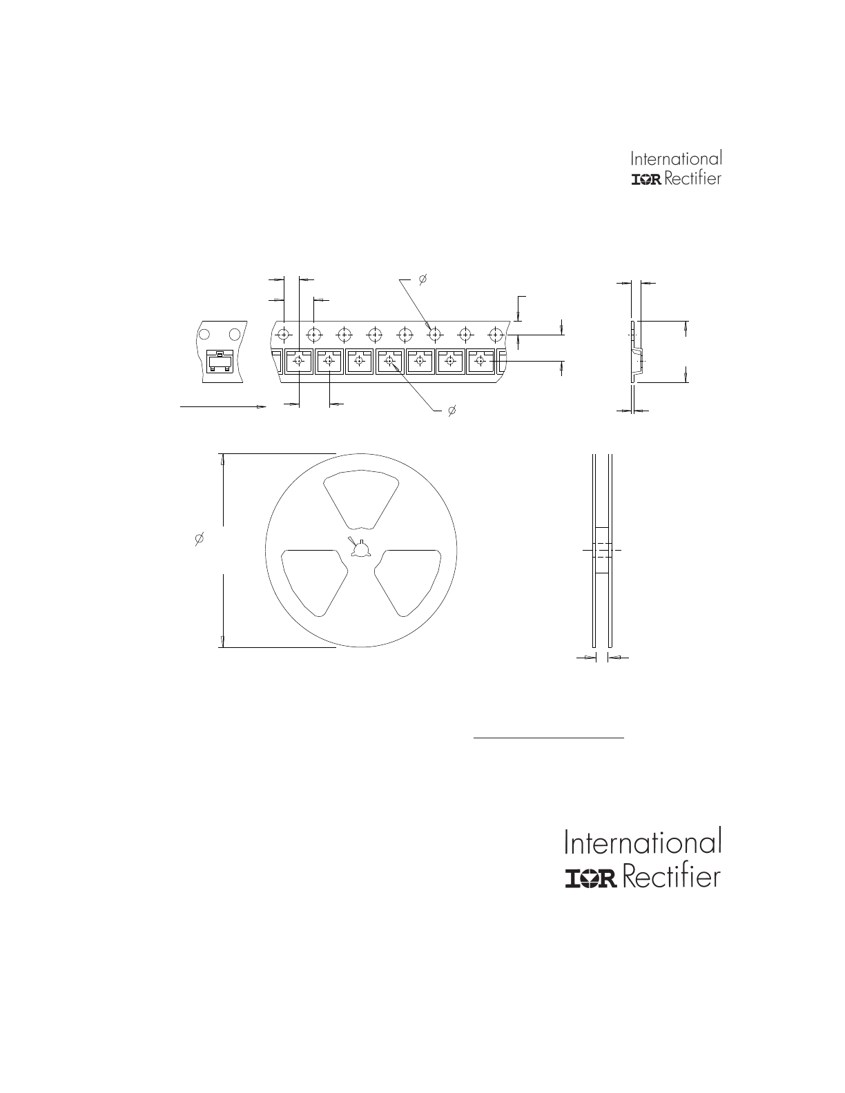
Micro3™ Tape & Reel Information
Dimensions are shown in millimeters (inches)
2.05 ( .080 )
1.95 ( .077 )
TR
FEED DIRECTION
4.1 ( .161 )
3.9 ( .154 )
1.6 ( .062 )
1.5 ( .060 )
1.85 ( .072 )
1.65 ( .065 )
3.55 ( .139 )
3.45 ( .136 )
1.1 ( .043 )
0.9 ( .036 )
4.1 ( .161 )
3.9 ( .154 )
0.35 ( .013 )
0.25 ( .010 )
8.3 ( .326 )
7.9 ( .312 )
1.32 ( .051 )
1.12 ( .045 )
9.90 ( .390 )
8.40 ( .331 )
178.00
( 7.008 )
MAX.
NOTES:
1. CONTROLLING DIMENSION : MILLIMETER.
2. OUTLINE CONFORMS TO EIA-481 & EIA-541.
Note: For the most current drawing please refer to IR website at http://www.irf.com/package
IR WORLD HEADQUARTERS: 101N.Sepulveda blvd, El Segundo, California 90245, USA Tel: (310) 252-7105
TAC Fax: (310) 252-7903
Visit us at www.irf.com for sales contact information. 09/2012