
IRLML0060TRPbF
1
2016-12-20
Absolute Maximum Ratings
Symbol Parameter
Max.
Units
V
DS
Drain-to-Source Voltage
60
V
I
D
@ T
A
= 25°C
Continuous Drain Current, V
GS
@ 10V
2.7
A
I
D
@ T
A
= 70°C
Continuous Drain Current, V
GS
@ 10V
2.1
I
DM
Pulsed Drain Current
11
P
D
@T
A
= 25°C
Maximum Power Dissipation
1.25
W
P
D
@T
A
= 70°C
Maximum Power Dissipation
0.80
Linear Derating Factor
0.01
mW/°C
V
GS
Gate-to-Source Voltage
± 16
T
J
Operating Junction and
°C
T
STG
Storage Temperature Range
-55 to + 150
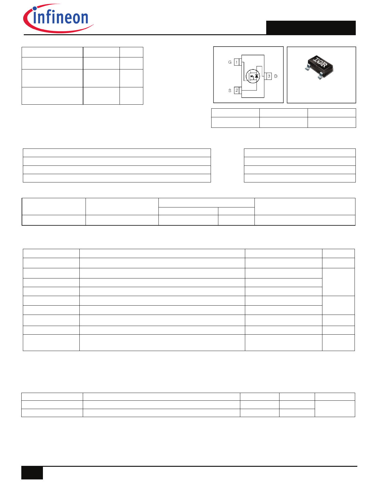
Micro 3™ (SOT-23)
IRLML0060TRPbF
G D S
Gate Drain Source
Base part number
Package Type
Standard Pack
Orderable Part Number
Form
Quantity
IRLML0060TRPbF
Micro 3™ (SOT-23)
Tape and Reel
3000
IRLML0060TRPbF
HEXFET
®
Power MOSFET
Thermal Resistance
Symbol Parameter
Typ.
Max.
Units
R
JA
Junction-to-Ambient –––
100
R
JA
Junction-to-Ambient (t < 10s) –––
99
°C/W
V
DSS
60
V
V
GS
±16
V
R
DS(on)
max
(@ V
GS
= 10V)
92
m
R
DS(on)
max
(@ V
GS
= 4.5V)
116
m
Applications
Load/System Switch
Features
Benefits
Industry-Standard Pinout
Multi-Vendor Compatibility
Compatible with Existing Surface Mount Techniques
results in Easier Manufacturing
RoHS Compliant Containing no Lead, no Bromide and no Halogen
Environmentally Friendlier
MSL1
Increased Reliability
IRLML0060TRPbF
2
2016-12-20
Notes:
Repetitive rating; pulse width limited by max. junction temperature.
Pulse width
400µs; duty cycle 2%.
Surface mounted on 1 in square Cu board
Refer to application note #AN-994.
Electrical Characteristics @ T
J
= 25°C (unless otherwise specified)
Parameter Min.
Typ.
Max.
Units
Conditions
V
(BR)DSS
Drain-to-Source Breakdown Voltage
60
––– –––
V V
GS
= 0V, I
D
= 250µA
V
(BR)DSS
/
T
J
Breakdown Voltage Temp. Coefficient
––– 0.06 ––– V/°C Reference to 25°C, I
D
= 1mA
R
DS(on)
Static Drain-to-Source On-Resistance
––– 98 116
m
V
GS
= 4.5V, I
D
= 2.2A
––– 78 92
V
GS
= 10V, I
D
= 2.7A
V
GS(th)
Gate Threshold Voltage
1.0
–––
2.5
V V
DS
= V
GS
, I
D
= 25µA
I
DSS
Drain-to-Source Leakage Current
––– ––– 20
µA
V
DS
= 60V, V
GS
= 0V
––– ––– 250
V
DS
= 60V,V
GS
= 0V,T
J
= 125°C
I
GSS
Gate-to-Source Forward Leakage
–––
––– 100
nA
V
GS
= 16V
Gate-to-Source Reverse Leakage
–––
––– -100
V
GS
= -16V
R
G
Internal Gate Resistance
–––
1.6
–––
gfs
Forward Trans conductance
7.6
––– –––
S V
DS
= 25V, I
D
= 2.7A
Q
g
Total Gate Charge
–––
2.5
–––
I
D
= 2.7A
Q
gs
Gate-to-Source Charge
–––
0.7
–––
V
DS
= 30V
Q
gd
Gate-to-Drain (‘Miller’) Charge
–––
1.3
–––
V
GS
= 4.5V
t
d(on)
Turn-On Delay Time
–––
5.4
–––
ns
V
DD
= 30V
t
r
Rise Time
–––
6.3
–––
I
D
= 1.0A
t
d(off)
Turn-Off Delay Time
–––
6.8
–––
R
G
= 6.8
t
f
Fall Time
–––
4.2
–––
V
GS
= 4.5V
C
iss
Input Capacitance
–––
290 –––
pF
V
GS
= 0V
C
oss
Output Capacitance
–––
37
–––
V
DS
= 25V
C
rss
Reverse Transfer Capacitance
–––
21
–––
ƒ = 1.0MHz
nC
Source-Drain Ratings and Characteristics
Parameter
Min. Typ. Max. Units
Conditions
I
S
Continuous Source Current
––– ––– 1.6
A
MOSFET symbol
(Body Diode)
showing the
I
SM
Pulsed Source Current
––– ––– 11
integral reverse
(Body Diode)
p-n junction diode.
V
SD
Diode Forward Voltage
–––
–––
1.3
V T
J
= 25°C,I
S
= 2.7A,V
GS
= 0V
t
rr
Reverse Recovery Time
–––
14
21
ns T
J
= 25°C ,V
R
= 30V, I
F
= 1.6A
Q
rr
Reverse Recovery Charge
–––
13
20
nC di/dt = 100A/µs
IRLML0060TRPbF
3
2016-12-20
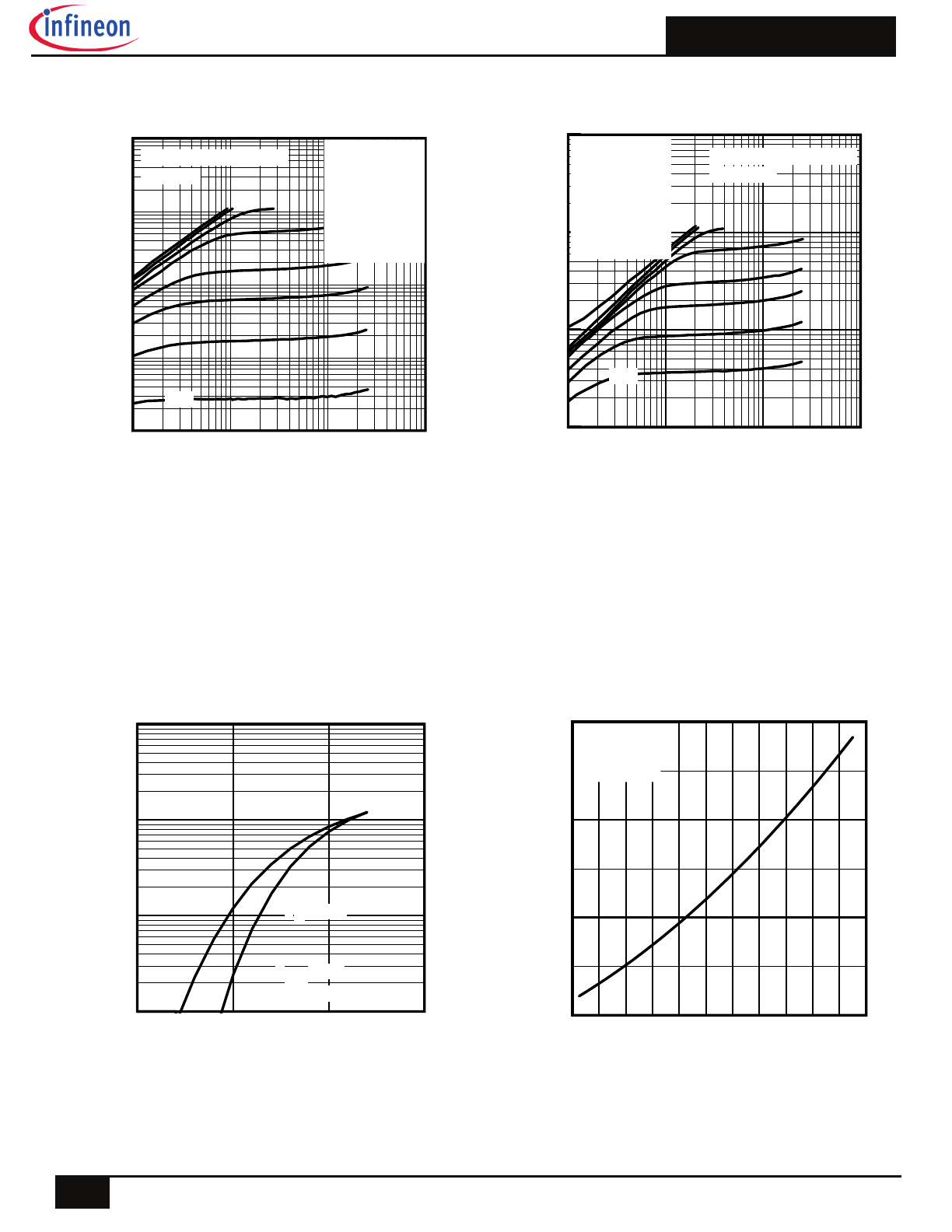
Fig. 2 Typical Output Characteristics
Fig. 3
Typical Transfer Characteristics
Fig. 4 Normalized On-Resistance
vs. Temperature
Fig. 1 Typical Output Characteristics
0.1
1
10
100
VDS, Drain-to-Source Voltage (V)
0.01
0.1
1
10
100
I D
, D
ra
in
-t
o-
S
ou
rc
e
C
u
rr
en
t (
A
)
VGS
TOP 10V
6.0V
4.5V
4.0V
3.5V
3.3V
3.0V
BOTTOM
2.8V
60µs PULSE WIDTH
Tj = 25°C
2.8V
0.1
1
10
100
VDS, Drain-to-Source Voltage (V)
0.1
1
10
100
I D
, D
ra
in
-t
o-
S
ou
rc
e
C
u
rr
en
t (
A
)
2.8V
60µs PULSE WIDTH
Tj = 150°C
VGS
TOP 10V
6.0V
4.5V
4.0V
3.5V
3.3V
3.0V
BOTTOM
2.8V
2
3
4
5
VGS, Gate-to-Source Voltage (V)
0.1
1
10
100
I D
, D
ra
in
-t
o-
S
ou
rc
e
C
ur
re
nt
(A
)
TJ = 25°C
TJ = 150°C
VDS = 25V
60µs PULSE WIDTH
-60 -40 -20 0 20 40 60 80 100 120 140 160
TJ , Junction Temperature (°C)
0.5
1.0
1.5
2.0
R
D
S
(o
n)
,
D
ra
in
-t
o-
S
ou
rc
e
O
n
R
es
is
ta
nc
e
(
N
or
m
al
iz
ed
)
ID = 2.7A
VGS = 10V
IRLML0060TRPbF
4
2016-12-20
Fig 5. Typical Capacitance vs.
Drain-to-Source Voltage
Fig 8. Maximum Safe Operating Area
Fig. 7 Typical Source-to-Drain Diode
Forward Voltage
Fig 6. Typical Gate Charge vs.
Gate-to-Source Voltage
0.1
1
10
100
VDS, Drain-to-Source Voltage (V)
10
100
1000
10000
C
, C
ap
ac
ita
nc
e
(p
F
)
VGS = 0V, f = 1 MHZ
Ciss = Cgs + Cgd, C ds SHORTED
Crss = Cgd
Coss = Cds + Cgd
Coss
Crss
Ciss
0
1
2
3
4
5
6
7
QG, Total Gate Charge (nC)
0.0
2.0
4.0
6.0
8.0
10.0
12.0
14.0
V
G
S
, G
at
e-
to
-S
ou
rc
e
V
ol
ta
ge
(
V
)
VDS= 48V
VDS= 30V
VDS= 12V
ID= 2.7A
0.2
0.4
0.6
0.8
1.0
1.2
VSD, Source-to-Drain Voltage (V)
0.1
1
10
100
I S
D
, R
ev
er
se
D
ra
in
C
ur
re
nt
(
A
)
TJ = 25°C
TJ = 150°C
VGS = 0V
0
1
10
100
VDS, Drain-to-Source Voltage (V)
0.01
0.1
1
10
100
I D
,
D
ra
in
-t
o-
S
ou
rc
e
C
ur
re
nt
(
A
)
OPERATION IN THIS AREA
LIMITED BY R DS(on)
TA = 25°C
Tj = 150°C
Single Pulse
100µsec
1msec
10msec
IRLML0060TRPbF
5
2016-12-20
Fig 11. Maximum Effective Transient Thermal Impedance, Junction-to-Ambient
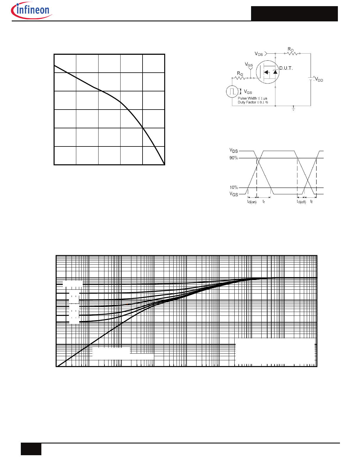
Fig 9. Maximum Drain Current vs. Case Temperature
Fig 10a. Switching Time Test Circuit
Fig 10b. Switching Time Waveforms
25
50
75
100
125
150
TA , Ambient Temperature (°C)
0.0
0.5
1.0
1.5
2.0
2.5
3.0
I D
,
D
ra
in
C
ur
re
nt
(
A
)
1E-006
1E-005
0.0001
0.001
0.01
0.1
1
10
100
t1 , Rectangular Pulse Duration (sec)
0.01
0.1
1
10
100
1000
T
he
rm
al
R
es
po
ns
e
(
Z
th
JA
)
°
C
/W
0.20
0.10
D = 0.50
0.02
0.01
0.05
SINGLE PULSE
( THERMAL RESPONSE )
Notes:
1. Duty Factor D = t1/t2
2. Peak Tj = P dm x Zthja + TA
IRLML0060TRPbF
6
2016-12-20
Fig 13. Typical On-Resistance Vs.
Drain Current
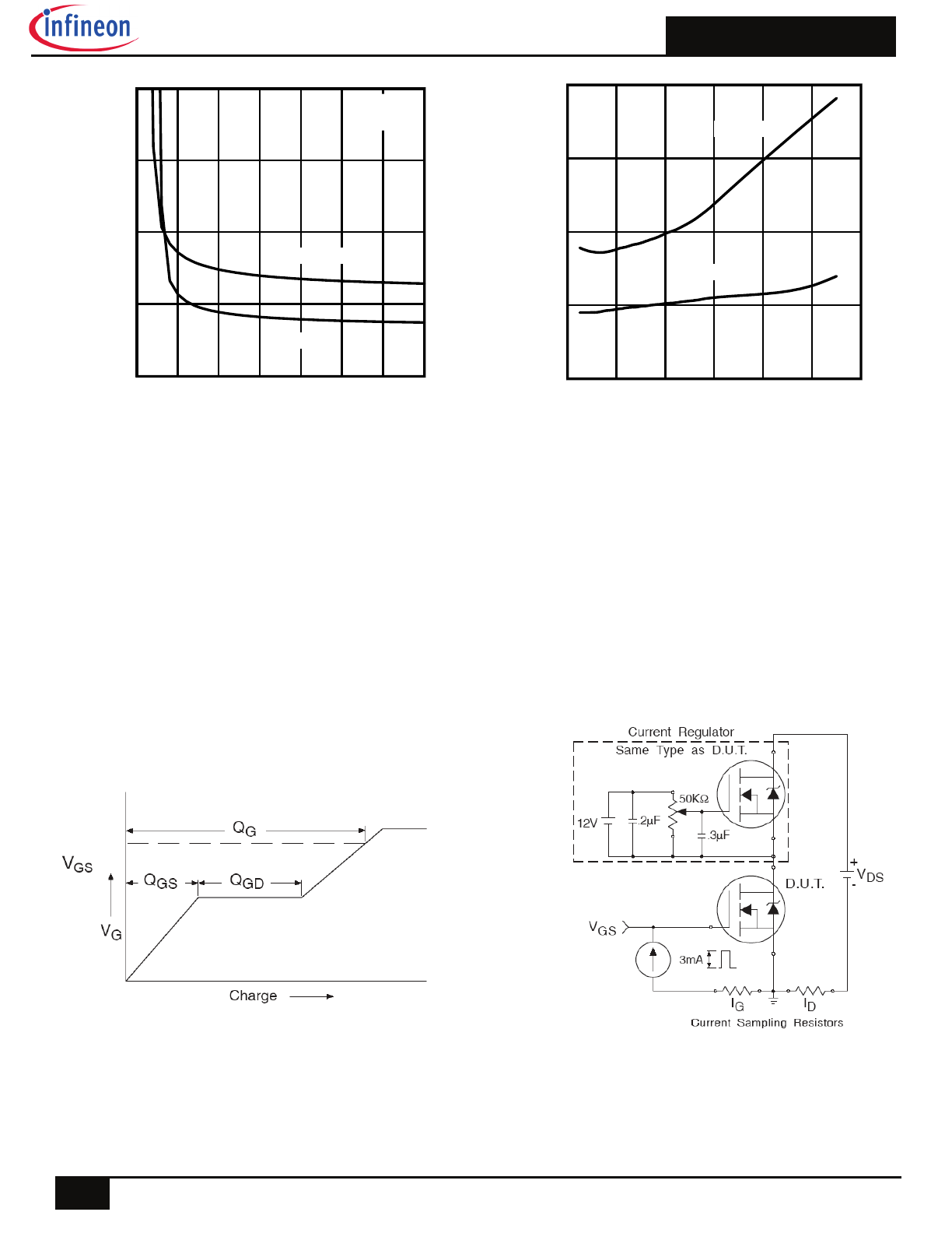
Fig 14a. Basic Gate Charge Waveform
Fig 12. Typical On-Resistance Vs.
Gate Voltage
Fig 14b. Gate Charge Test Circuit
3
4
5
6
7
8
9
10
VGS, Gate -to -Source Voltage (V)
0
100
200
300
400
R
D
S
(o
n
),
D
ra
in
-t
o
-
S
o
ur
ce
O
n
R
e
si
st
a
n
ce
(
m
)
ID = 2.7A
TJ = 25°C
TJ = 125°C
0
2
4
6
8
10
12
ID, Drain Current (A)
50
75
100
125
150
R
D
S
(o
n)
,
D
ra
in
-t
o
-S
ou
rc
e
O
n
R
es
is
ta
nc
e
(
m
)
Vgs = 10V
Vgs = 4.5V
IRLML0060TRPbF
7
2016-12-20
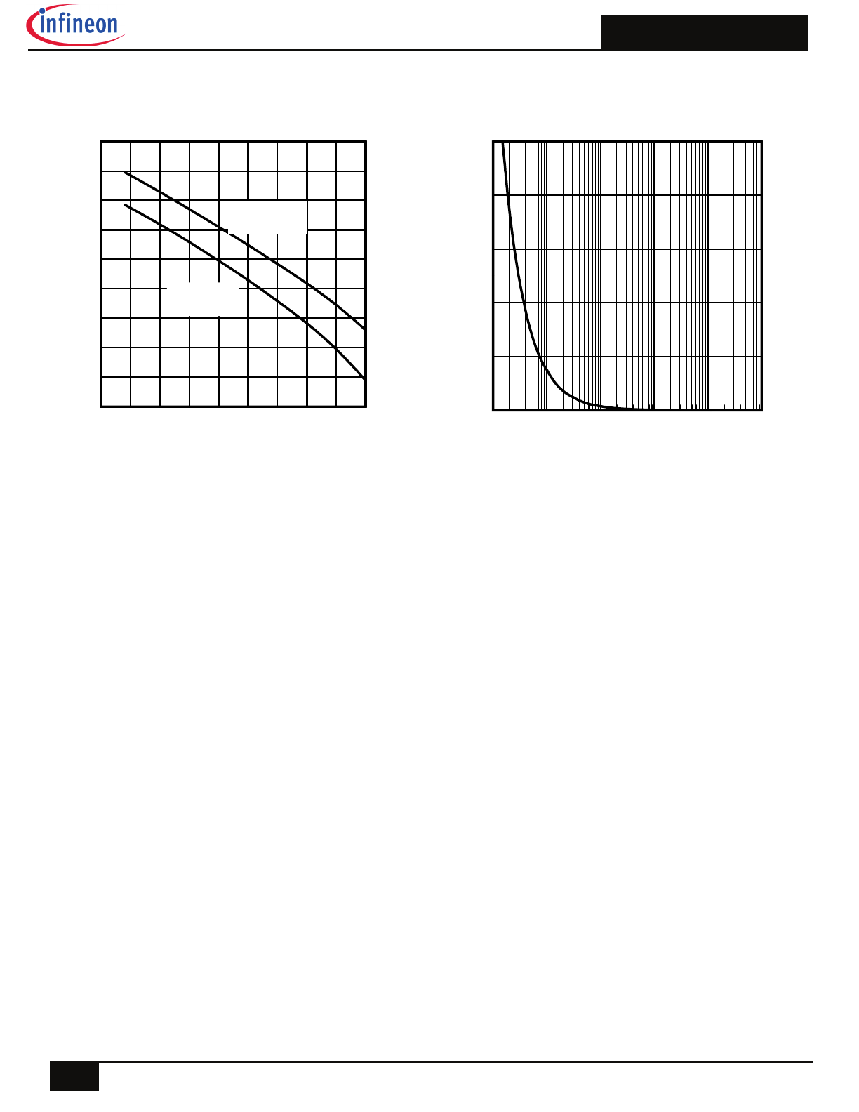
Fig 15. Typical Threshold Voltage Vs.
Junction Temperature
Fig 16. Typical Power Vs. Time
-75 -50 -25
0
25
50
75 100 125 150
TJ , Temperature ( °C )
1.0
1.2
1.4
1.6
1.8
2.0
2.2
2.4
2.6
2.8
V
G
S
(t
h)
, G
at
e
th
re
sh
ol
d
V
ol
ta
ge
(
V
)
ID = 25µA
ID = 250µA
1
10
100
1000
10000
100000
Time (sec)
0
20
40
60
80
100
P
ow
er
(
W
)
IRLML0060TRPbF
8
2016-12-20
Note: For the most current drawing please refer to Infineon’s web site
www.infineon.com
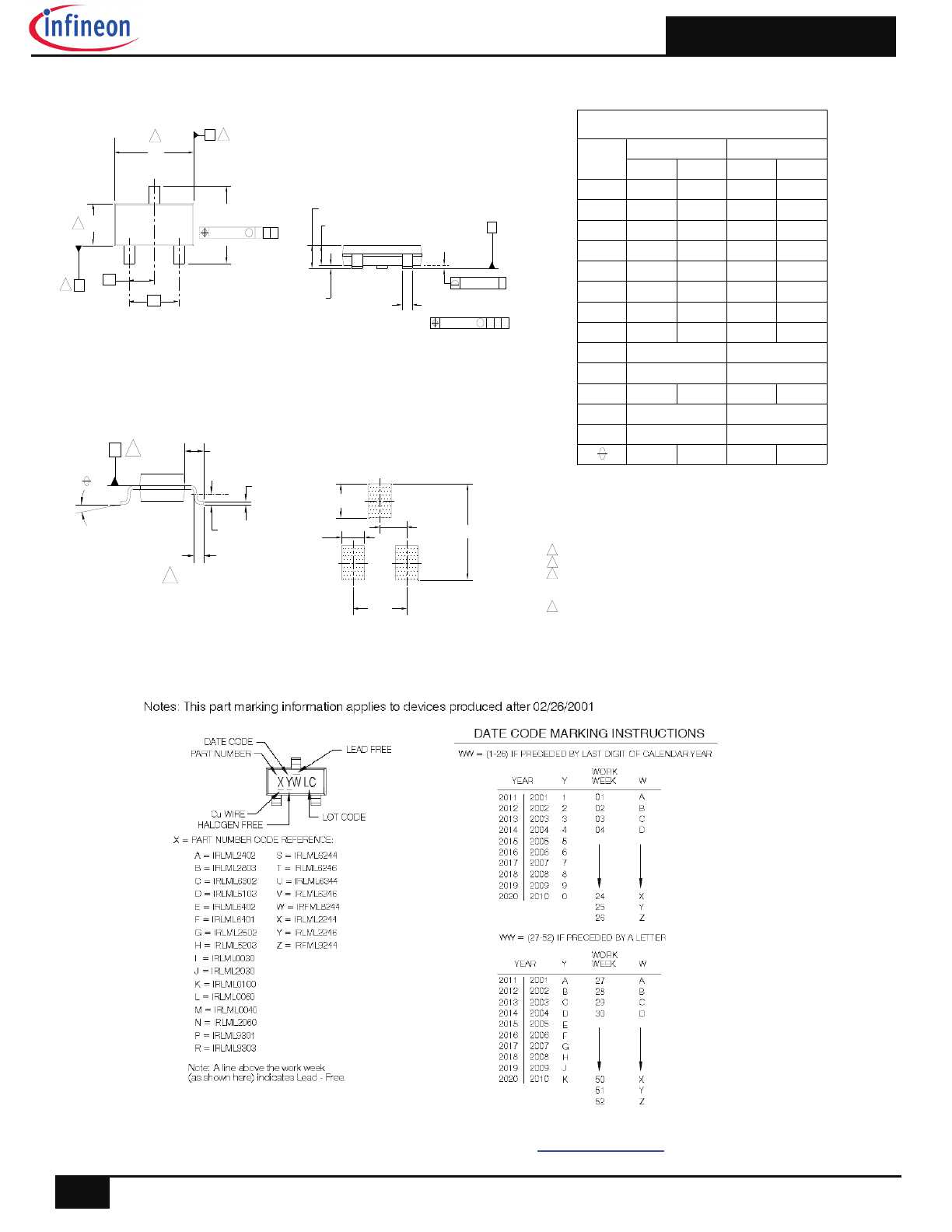
Micro3™ (SOT-23/TO-236AB) Part Marking Information
Micro3™ (SOT-23) Package Outline (Dimensions are shown in millimeters (inches))
e
E1
E
D
A
B
0.15 [0.006]
e1
1
2
3
M C B A
5
6
6
5
NOTES:
1. DIMENSIONING & TOLERANCING PER ANSI Y14.5M-1994
2. DIMENSIONS ARE SHOWN IN MILLIMETERS [INCHES].
3. CONTROLLING DIMENSION: MILLIMETER.
4. DATUM PLANE H IS LOCATED AT THE MOLD PARTING LINE.
5. DATUM A AND B TO BE DETERMINED AT DATUM PLANE H.
6. DIMENSIONS D AND E1 ARE MEASURED AT DATUM PLANE H. DIMENSIONS DOES
NOT INCLUDE MOLD PROTRUSIONS OR INTERLEAD FLASH. MOLD PROTRUSIONS
OR INTERLEAD FLASH SHALL NOT EXCEED 0.25 MM [0.010 INCH] PER SIDE.
7. DIMENSION L IS THE LEAD LENGTH FOR SOLDERING TO A SUBSTRATE.
8. OUTLINE CONFORMS TO JEDEC OUTLINE TO-236 AB.
NOTES:
b
A1
3X
A
A2
A
B
C
M
0.20 [0.008]
0.10 [0.004] C
C
3X L
c
L2
H 4
L1
7
0.972
1.900
Recommended Footprint
0.802
0.950
2.742
0.89
1.12
SYMBOL
MAX
MIN
A1
b
0.01
0.10
c
0.30
0.50
D
0.08
0.20
E
2.80
3.04
E1
2.10
2.64
e
1.20
1.40
A
0.95
BSC
L
0.40
0.60
0
8
MILLIMETERS
A2
0.88
1.02
e1
1.90
BSC
REF
0.54
L1
BSC
0.25
L2
0.010
BSC
0.021
REF
BSC
0.075
0.040
0.035
INCHES
8
0
0.024
0.016
BSC
0.037
0.055
0.047
0.104
0.083
0.120
0.110
0.008
0.003
0.020
0.012
0.004
0.0004
MIN
MAX
0.044
0.035
DIMENSIONS
IRLML0060TRPbF
9
2016-12-20
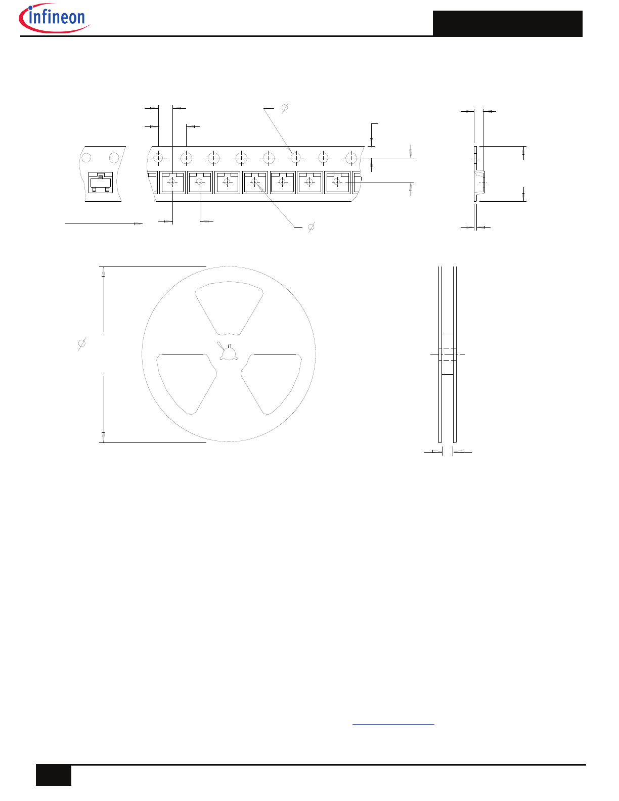
Micro3™
Tape & Reel Information (Dimensions are shown in millimeters (inches))
Note: For the most current drawing please refer to Infineon’s web site
www.infineon.com
2.05 ( .080 )
1.95 ( .077 )
TR
FEED DIRECTION
4.1 ( .161 )
3.9 ( .154 )
1.6 ( .062 )
1.5 ( .060 )
1.85 ( .072 )
1.65 ( .065 )
3.55 ( .139 )
3.45 ( .136 )
1.1 ( .043 )
0.9 ( .036 )
4.1 ( .161 )
3.9 ( .154 )
0.35 ( .013 )
0.25 ( .010 )
8.3 ( .326 )
7.9 ( .312 )
1.32 ( .051 )
1.12 ( .045 )
9.90 ( .390 )
8.40 ( .331 )
178.00
( 7.008 )
MAX.
NOTES:
1. CONTROLLING DIMENSION : MILLIMETER.
2. OUTLINE CONFORMS TO EIA-481 & EIA-541.
IRLML0060TRPbF
10
2016-12-20
Revision History
Date Comments
12/20/16
Changed datasheet with Infineon logo - all pages.
Removed typo “Industrial” on Feature and Benefits Table on page1.
Corrected typo for Igss test condition from “V
GS
= 20V” to “V
GS
= 16V” on page 2.
Qualification Information
Qualification Level
Consumer
(per JEDEC JESD47F)
†
Moisture Sensitivity Level
Micro3™ (SOT-23)
MSL1
(per JEDEC J-STD-020D)
†
RoHS Compliant
Yes
† Applicable version of JEDEC standard at the time of product release.
Trademarks of Infineon Technologies AG
µHVIC™, µIPM™, µPFC™, AU-ConvertIR™, AURIX™, C166™, CanPAK™, CIPOS™, CIPURSE™, CoolDP™, CoolGaN™, COOLiR™, CoolMOS™, CoolSET™,
CoolSiC™, DAVE™, DI-POL™, DirectFET™, DrBlade™, EasyPIM™, EconoBRIDGE™, EconoDUAL™, EconoPACK™, EconoPIM™, EiceDRIVER™, eupec™, FCOS™,
GaNpowIR™, HEXFET™, HITFET™, HybridPACK™, iMOTION™, IRAM™, ISOFACE™, IsoPACK™, LEDrivIR™, LITIX™, MIPAQ™, ModSTACK™, my-d™, NovalithIC™,
OPTIGA™, OptiMOS™, ORIGA™, PowIRaudio™, PowIRStage™, PrimePACK™, PrimeSTACK™, PROFET™, PRO-SIL™, RASIC™, REAL3™, SmartLEWIS™, SOLID
FLASH™, SPOC™, StrongIRFET™, SupIRBuck™, TEMPFET™, TRENCHSTOP™, TriCore™, UHVIC™, XHP™, XMC™
Trademarks updated November 2015
Other Trademarks
All referenced product or service names and trademarks are the property of their respective owners.
Edition 2016-04-19
Published by
Infineon Technologies AG
81726 Munich, Germany
© 2016 Infineon Technologies AG.
All Rights Reserved.
Do you have a question about this
document?
Email:
erratum@infineon.com
Document reference
ifx1
IMPORTANT NOTICE
The information given in this document shall in no
event be regarded as a guarantee of conditions or
characteristics (“Beschaffenheitsgarantie”) .
With respect to any examples, hints or any typical
values stated herein and/or any information
regarding the application of the product, Infineon
Technologies hereby disclaims any and all
warranties and liabilities of any kind, including
without limitation warranties of non-infringement
of intellectual property rights of any third party.
In addition, any information given in this
document is subject to customer’s compliance
with its obligations stated in this document and
any applicable legal requirements, norms and
standards concerning customer’s products and
any use of the product of Infineon Technologies in
customer’s applications.
The data contained in this document is exclusively
intended for technically trained staff. It is the
responsibility of customer’s technical
departments to evaluate the suitability of the
product for the intended application and the
completeness of the product information given in
this document with respect to such application.
For further information on the product, technology,
delivery terms and conditions and prices please
contact your nearest Infineon Technologies office
(
www.infineon.com
).
Please note that this product is not qualified
according to the AEC Q100 or AEC Q101 documents
of the Automotive Electronics Council.
WARNINGS
Due to technical requirements products may
contain dangerous substances. For information on
the types in question please contact your nearest
Infineon Technologies office.
Except as otherwise explicitly approved by Infineon
Technologies in a written document signed by
authorized representatives of Infineon
Technologies, Infineon Technologies’ products
may not be used in any applications where a
failure of the product or any consequences of the
use thereof can reasonably be expected to result in
personal injury.