
02/29/12
IRLML0040TRPbF
HEXFET
®
Power MOSFET
www.irf.com
1
ORDERING INFORMATION:
See detailed ordering and shipping information on the last page of this data sheet.
Notes
through
are on page 10
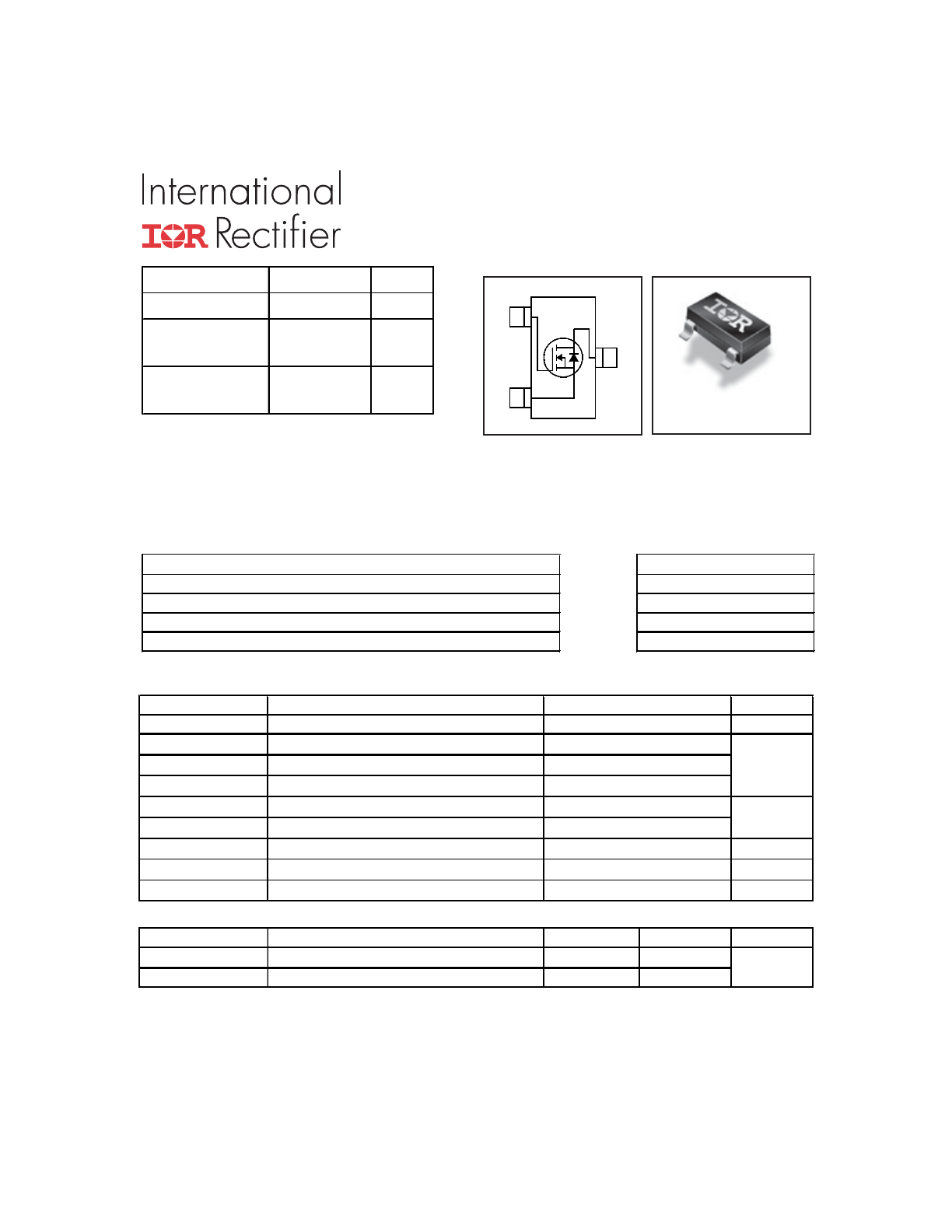
Micro3
TM
(SOT-23)
IRLML0040TRPbF
D
S
G
3
1
2
Features and Benefits
Application(s)
• Load/ System Switch
• DC Motor Drive
Features
Benefits
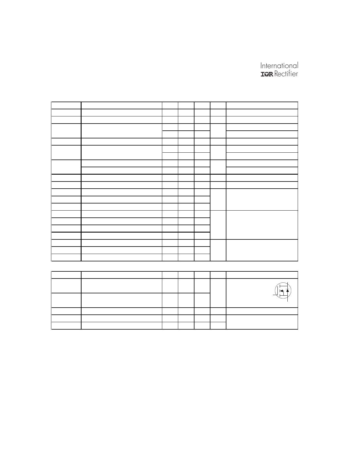
Absolute Maximum Ratings
Symbol
Parameter
Units
V
DS
Drain-Source Voltage
V
I
D
@ T
A
= 25°C
Continuous Drain Current, V
GS
@ 10V
I
D
@ T
A
= 70°C
Continuous Drain Current, V
GS
@ 10V
I
DM
Pulsed Drain Current
P
D
@T
A
= 25°C
Maximum Power Dissipation
P
D
@T
A
= 70°C
Maximum Power Dissipation
Linear Derating Factor
W/°C
V
GS
Gate-to-Source Voltage
V
T
J,
T
STG
Junction and Storage Temperature Range
°C
Thermal Resistance
Symbol
Parameter
Typ.
Max.
Units
R
θJA
Junction-to-Ambient
e
–––
100
R
θJA
Junction-to-Ambient (t<10s)
f
–––
99
°C/W
Max.
3.6
2.9
-55 to + 150
± 16
0.01
40
A
1.3
0.8
15
W
V
DSS
40
V
V
GS Max
± 16
V
R
DS(on)
max
(@V
GS
= 10V)
56
mΩ
R
DS(on) max
(@V
GS
= 4.5V)
78
mΩ
Low R
DS(on)
(
≤ 56mΩ)
Lower switching losses
Industry-standard pinout
Multi-vendor compatibility
Compatible with existing Surface Mount Techniques
results in Easier manufacturing
RoHS compliant containing no lead, no bromide and no halogen
⇒
Environmentally friendly
MSL1, Consumer qualification
Increased reliability
PD - 96309A
IRLML0040TRPbF
2
www.irf.com
D
S
G
Electric Characteristics @ T
J
= 25°C (unless otherwise specified)
Symbol
Parameter
Min. Typ. Max. Units
V
(BR)DSS
Drain-to-Source Breakdown Voltage
40
–––
–––
V
ΔV
(BR)DSS
/
ΔT
J
Breakdown Voltage Temp. Coefficient
–––
0.04
–––
V/°C
–––
44
56
–––
62
78
V
GS(th)
Gate Threshold Voltage
1.0
1.8
2.5
V
I
DSS
–––
–––
20
–––
–––
250
I
GSS
Gate-to-Source Forward Leakage
–––
–––
100
Gate-to-Source Reverse Leakage
–––
–––
-100
R
G
Internal Gate Resistance
–––
1.1
–––
Ω
gfs
Forward Transconductance
6.2
–––
–––
S
Q
g
Total Gate Charge
–––
2.6
3.9
Q
gs
Gate-to-Source Charge
–––
0.7
–––
Q
gd
Gate-to-Drain ("Miller") Charge
–––
1.4
–––
t
d(on)
Turn-On Delay Time
–––
5.1
–––
t
r
Rise Time
–––
5.4
–––
t
d(off)
Turn-Off Delay Time
–––
6.4
–––
t
f
Fall Time
–––
4.3
–––
C
iss
Input Capacitance
–––
266
–––
C
oss
Output Capacitance
–––
49
–––
C
rss
Reverse Transfer Capacitance
–––
29
–––
Source - Drain Ratings and Characteristics
Symbol Parameter
Min. Typ. Max. Units
I
S
Continuous Source Current
(Body Diode)
I
SM
Pulsed Source Current
(Body Diode)
c
V
SD
Diode Forward Voltage
–––
–––
1.2
V
t
rr
Reverse Recovery Time
–––
10
–––
ns
Q
rr
Reverse Recovery Charge
–––
9.3
–––
nC
Static Drain-to-Source On-Resistance
m
Ω
R
DS(on)
V
GS
= 4.5V, I
D
= 2.9A
d
di/dt = 100A/μs
d
V
GS
= 16V
V
GS
= -16V
T
J
= 25°C, V
R
= 32V, I
F
= 1.3 A
MOSFET symbol
showing the
V
DS
= 20V
Conditions
V
GS
= 4.5V
V
GS
= 0V
V
DS
= 25V
ƒ = 1.0MHz
T
J
= 25°C, I
S
= 1.3A, V
GS
= 0V
d
integral reverse
p-n junction diode.
Conditions
V
GS
= 0V, I
D
= 250μA
Reference to 25°C, I
D
= 1mA
V
GS
= 10V, I
D
= 3.6A
d
V
DS
= V
GS
, I
D
= 25μA
V
DS
= 40V, V
GS
= 0V
V
DS
= 40V, V
GS
= 0V, T
J
= 125°C
Drain-to-Source Leakage Current
μA
V
DS
= 10V, I
D
= 3.6A
I
D
= 3.6A
nA
nC
I
D
= 1.0A
R
G
= 6.8
Ω
V
GS
= 4.5V
d
V
DD
= 20V
ns
pF
A
1.3
15
–––
–––
–––
–––
IRLML0040TRPbF
www.irf.com
3
Fig 3. Typical Transfer Characteristics
Fig 2. Typical Output Characteristics
Fig 1. Typical Output Characteristics
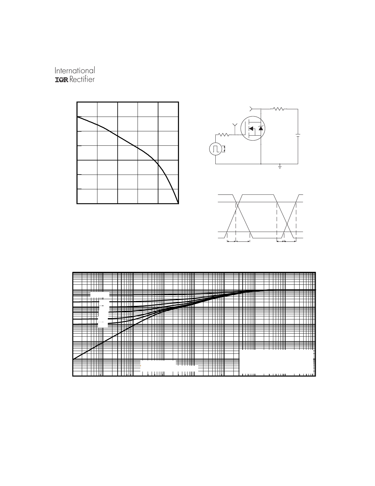
Fig 4. Normalized On-Resistance
Vs. Temperature
0.1
1
10
100
VDS, Drain-to-Source Voltage (V)
0.001
0.01
0.1
1
10
100
I D
, D
ra
in
-t
o-
S
ou
rc
e
C
ur
re
nt
(
A
)
VGS
TOP
10V
7.0V
6.0V
4.5V
4.0V
3.5V
3.0V
BOTTOM
2.5V
≤60μs PULSE WIDTH Tj = 25°C
2.5V
0.1
1
10
100
VDS, Drain-to-Source Voltage (V)
0.1
1
10
100
I D
, D
ra
in
-t
o-
S
ou
rc
e
C
ur
re
nt
(
A
)
2.5V
≤60μs PULSE WIDTH
Tj = 150°C
VGS
TOP
10V
7.0V
6.0V
4.5V
4.0V
3.5V
3.0V
BOTTOM
2.5V
2.0
3.0
4.0
5.0
VGS, Gate-to-Source Voltage (V)
0.1
1
10
100
I D
, D
ra
in
-t
o-
S
ou
rc
e
C
ur
re
nt
(
A
)
TJ = 25°C
TJ = 150°C
VDS = 25V
≤60μs PULSE WIDTH
-60 -40 -20 0 20 40 60 80 100 120 140 160
TJ , Junction Temperature (°C)
0.5
1.0
1.5
2.0
R
D
S
(o
n)
,
D
ra
in
-t
o-
S
ou
rc
e
O
n
R
es
is
ta
nc
e
(
N
or
m
al
iz
ed
)
ID = 3.6A
VGS = 10V
IRLML0040TRPbF
4
www.irf.com
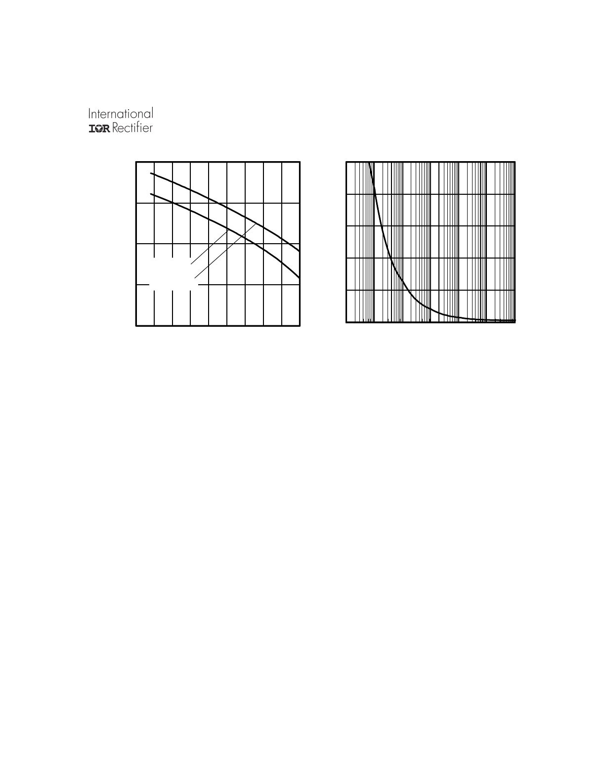
Fig 6. Typical Gate Charge Vs.
Gate-to-Source Voltage
Fig 5. Typical Capacitance Vs.
Drain-to-Source Voltage
Fig 8. Maximum Safe Operating Area
Fig 7. Typical Source-Drain Diode
Forward Voltage
1
10
100
VDS, Drain-to-Source Voltage (V)
10
100
1000
10000
C
, C
ap
ac
ita
nc
e
(p
F
)
VGS = 0V, f = 1 MHZ
Ciss = Cgs + Cgd, C ds SHORTED
Crss = Cgd
Coss = Cds + Cgd
Coss
Crss
Ciss
0.3
0.5
0.7
0.9
1.1
VSD, Source-to-Drain Voltage (V)
0.1
1
10
100
I S
D
, R
ev
er
se
D
ra
in
C
ur
re
nt
(
A
)
TJ = 25°C
TJ = 150°C
VGS = 0V
0
1
10
100
VDS, Drain-to-Source Voltage (V)
0.01
0.1
1
10
100
I D
,
D
ra
in
-t
o-
S
ou
rc
e
C
ur
re
nt
(
A
)
OPERATION IN THIS AREA
LIMITED BY R DS(on)
TA = 25°C
Tj = 150°C
Single Pulse
100μsec
1msec
10msec
0
1
2
3
4
5
6
7
QG, Total Gate Charge (nC)
0
2
4
6
8
10
12
14
V
G
S
, G
at
e-
to
-S
ou
rc
e
V
ol
ta
ge
(
V
)
VDS= 32V
VDS= 20V
VDS= 8V
ID= 3.6A
IRLML0040TRPbF
www.irf.com
5
Fig 11. Typical Effective Transient Thermal Impedance, Junction-to-Ambient
Fig 9. Maximum Drain Current Vs.
Ambient Temperature
V
DS
90%
10%
V
GS
t
d(on)
t
r
t
d(off)
t
f
Fig 10b. Switching Time Waveforms
Fig 10a. Switching Time Test Circuit
V
DS
Pulse Width ≤ 1 µs
Duty Factor ≤ 0.1 %
R
D
V
GS
R
G
D.U.T.
V
GS
+
-
V
DD
25
50
75
100
125
150
TA , Ambient Temperature (°C)
0
0.6
1.2
1.8
2.4
3
3.6
4.2
I D
,
D
ra
in
C
ur
re
nt
(
A
)
1E-006
1E-005
0.0001
0.001
0.01
0.1
1
10
100
t1 , Rectangular Pulse Duration (sec)
0.001
0.01
0.1
1
10
100
1000
T
he
rm
al
R
es
po
ns
e
(
Z
th
JA
)
°C
/W
0.20
0.10
D = 0.50
0.02
0.01
0.05
SINGLE PULSE
( THERMAL RESPONSE )
Notes:
1. Duty Factor D = t1/t2
2. Peak Tj = P dm x Zthja + TA
IRLML0040TRPbF
6
www.irf.com
Fig 13. Typical On-Resistance Vs. Drain
Current
Fig 12. Typical On-Resistance Vs. Gate
Voltage
Fig 14b. Gate Charge Test Circuit
Fig 14a. Basic Gate Charge Waveform
Q
G
Q
GS
Q
GD
V
G
Charge
V
GS
D.U.T.
V
DS
I
D
I
G
3mA
V
GS
.3
μF
50K
Ω
.2
μF
12V
Current Regulator
Same Type as D.U.T.
Current Sampling Resistors
+
-
2
4
6
8
10
12
14
16
VGS, Gate -to -Source Voltage (V)
20
40
60
80
100
120
140
160
R
D
S
(o
n)
,
D
ra
in
-t
o
-S
ou
rc
e
O
n
R
es
is
ta
nc
e
(m
Ω
)
ID = 3.6A
TJ = 25°C
TJ = 125°C
0
5
10
15
20
25
30
35
ID, Drain Current (A)
0
50
100
150
200
250
R
D
S
(o
n)
,
D
ra
in
-t
o
-S
ou
rc
e
O
n
R
es
is
ta
nc
e
(m
Ω
)
Vgs = 10V
Vgs = 4.5V
IRLML0040TRPbF
www.irf.com
7
Fig 15. Typical Threshold Voltage Vs.
Junction Temperature
Fig 16. Typical Power Vs. Time
-75 -50 -25
0
25
50
75 100 125 150
TJ , Temperature ( °C )
0.5
1.0
1.5
2.0
2.5
V
G
S
(t
h)
, G
at
e
th
re
sh
ol
d
V
ol
ta
ge
(
V
)
ID = 25uA
ID = 250uA
1E-005 0.0001 0.001
0.01
0.1
1
10
Time (sec)
0
20
40
60
80
100
P
ow
er
(
W
)
IRLML0040TRPbF
8
www.irf.com
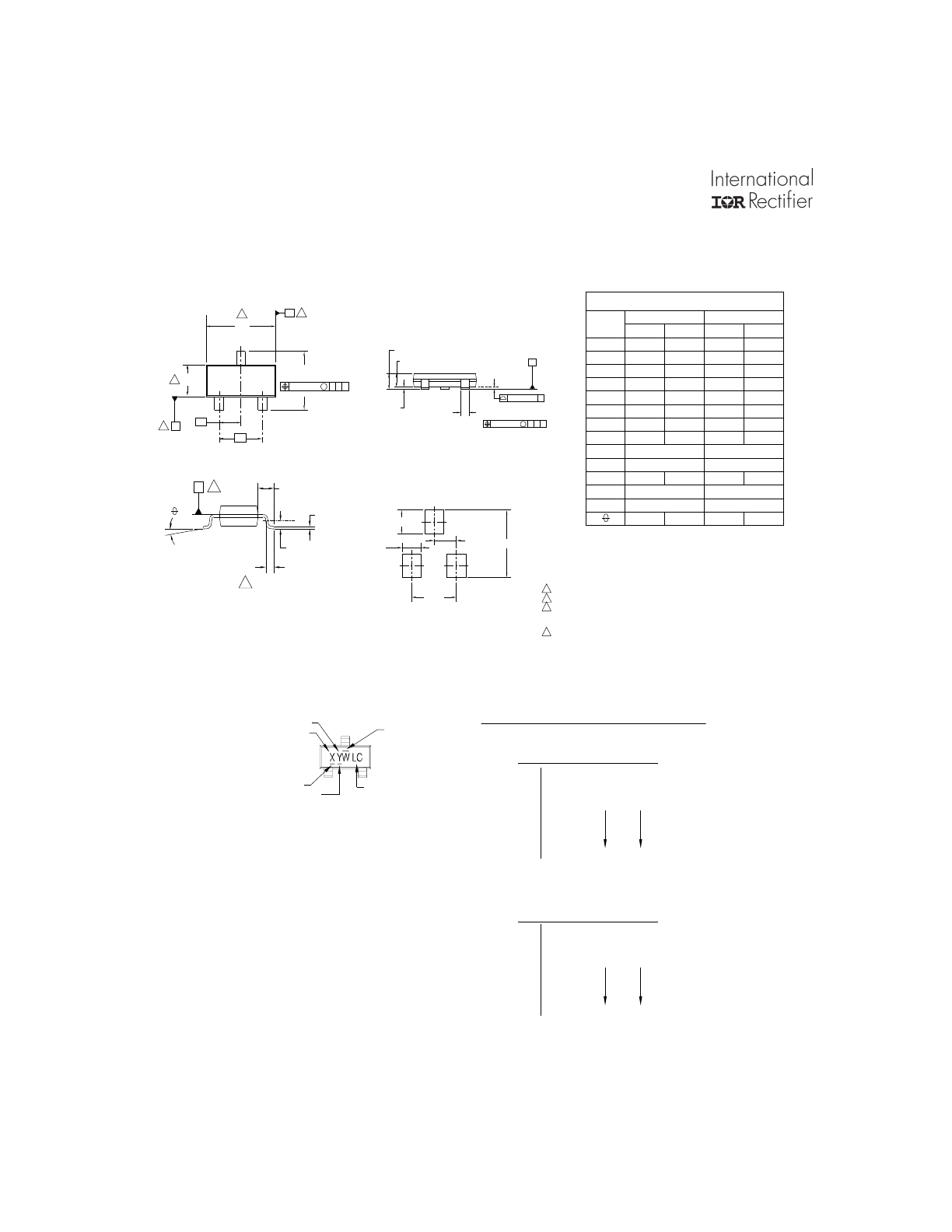
Micro3 (SOT-23/TO-236AB) Part Marking Information
Micro3 (SOT-23) Package Outline
Dimensions are shown in millimeters (inches)
Note: For the most current drawing please refer to IR website at: http://www.irf.com/package/
e
E1
E
D
A
B
0.15 [0.006]
e1
1
2
3
M C B A
5
6
6
5
NOTES:
b
A1
3X
A
A2
A
B
C
M
0.20 [0.008]
0.10 [0.004] C
C
1. DIMENSIONING & TOLERANCING PER ANSI Y14.5M-1994
2. DIMENSIONS ARE SHOWN IN MILLIMETERS [INCHES].
3. CONTROLLING DIMENSION: MILLIMETER.
4. DATUM PLANE H IS LOCATED AT THE MOLD PARTING LINE.
5. DATUM A AND B TO BE DETERMINED AT DATUM PLANE H.
6. DIMENSIONS D AND E1 ARE MEASURED AT DATUM PLANE H. DIMENSIONS DOES
NOT INCLUDE MOLD PROTRUSIONS OR INTERLEAD FLASH. MOLD PROTRUSIONS
OR INTERLEAD FLASH SHALL NOT EXCEED 0.25 MM [0.010 INCH] PER SIDE.
7. DIMENSION L IS THE LEAD LENGTH FOR SOLDERING TO A SUBSTRATE.
8. OUTLINE CONFORMS TO JEDEC OUTLINE TO-236 AB.
0.89
1.12
SYMBOL
MAX
MIN
A1
b
0.01
0.10
c
0.30
0.50
D
0.08
0.20
E
2.80
3.04
E1
2.10
2.64
e
1.20
1.40
A
0.95
BSC
L
0.40
0.60
0
8
MILLIMETERS
A2
0.88
1.02
e1
1.90
BSC
REF
0.54
L1
BSC
0.25
L2
BSC
REF
%6&
INCHES
8
0
%6&
0.0004
MIN
MAX
DIMENSIONS
0.972
1.900
Recommended Footprint
0.802
0.950
2.742
3X L
c
L2
H 4
L1
7
Notes : This part marking information applies to devices produced after 02/26/2001
WW = (27-52) IF PRECEDED BY A LETTER
C
H
K
J
E
F
G
D
0
2010
YEAR
B
A
Y
2007
2008
2009
2006
2005
2003
2004
2001
2002
5
7
9
8
6
3
4
1
2
C
29
Z
52
50
51
X
Y
30
D
X
24
W
WORK
WEEK
27
28
B
A
26
25
Z
Y
03
04
01
02
C
D
A
B
DATE CODE MARKING INSTRUCTIONS
WW = (1-26) IF PRECEDED BY LAST DIGIT OF CALENDAR YEAR
YEAR
Y
W
WEEK
WORK
2020
2017
2018
2019
2016
2015
2013
2014
2011
2012
2010
2007
2008
2009
2006
2005
2003
2004
2001
2002
2020
2017
2018
2019
2016
2015
2013
2014
2011
2012
F = IRLML6401
LOT CODE
LEAD FREE
DATE CODE
E = IRLML6402
X = PART NUMBER CODE REFERENCE:
D = IRLML5103
C = IRLML6302
B = IRLML2803
A = IRLML2402
H = IRLML5203
G = IRLML2502
Note: A line above the work week
(as shown here) indicates Lead - Free.
I = IRLML0030
J = IRLML2030
L = IRLML0060
M = IRLML0040
K = IRLML0100
N = IRLML2060
P = IRLML9301
R = IRLML9303
Cu WIRE
HALOGEN FREE
PART NUMBER
X = IRLML2244
W = IRFML8244
V = IRLML6346
U = IRLML6344
T = IRLML6246
S = IRLML6244
Z = IRFML9244
Y = IRLML2246
IRLML0040TRPbF
www.irf.com
9
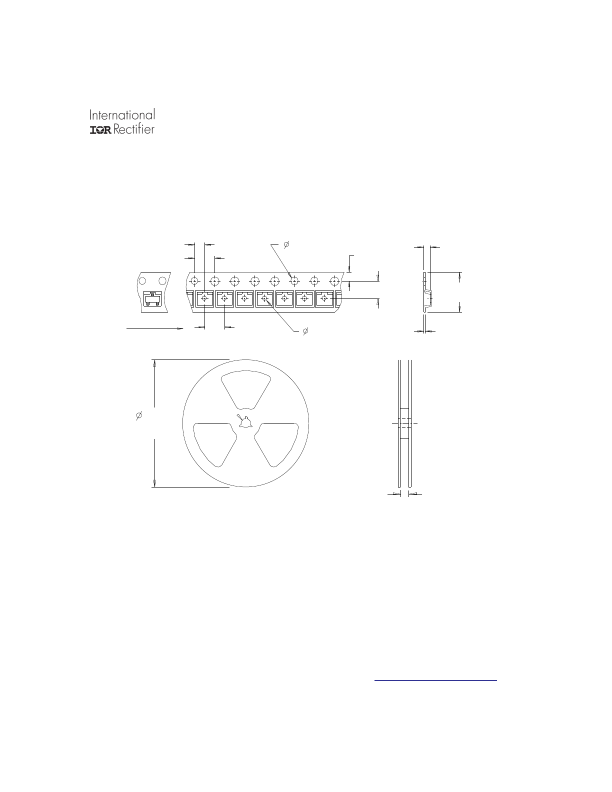
Micro3™ (SOT-23) Tape & Reel Information
Dimensions are shown in millimeters (inches)
2.05 ( .080 )
1.95 ( .077 )
TR
FEED DIRECTION
4.1 ( .161 )
3.9 ( .154 )
1.6 ( .062 )
1.5 ( .060 )
1.85 ( .072 )
1.65 ( .065 )
3.55 ( .139 )
3.45 ( .136 )
1.1 ( .043 )
0.9 ( .036 )
4.1 ( .161 )
3.9 ( .154 )
0.35 ( .013 )
0.25 ( .010 )
8.3 ( .326 )
7.9 ( .312 )
1.32 ( .051 )
1.12 ( .045 )
9.90 ( .390 )
8.40 ( .331 )
178.00
( 7.008 )
MAX.
NOTES:
1. CONTROLLING DIMENSION : MILLIMETER.
2. OUTLINE CONFORMS TO EIA-481 & EIA-541.
Note: For the most current drawing please refer to IR website at:
http://www.irf.com/package/
IRLML0040TRPbF
10
www.irf.com
Data and specifications subject to change without notice.
Qualification standards can be found at International Rectifier’s web site
http://www.irf.com/product-info/reliability
Higher qualification ratings may be available should the user have such requirements.
Please contact your International Rectifier sales representative for further information:
http://www.irf.com/whoto-call/salesrep/
Applicable version of JEDEC standard at the time of product release.
Notes:
Repetitive rating; pulse width limited by max. junction temperature.
Pulse width ≤ 400μs; duty cycle ≤ 2%.
Surface mounted on 1 in square Cu board
Refer to
application note #AN-994.
Note
Form
Quantity
IRLML0040TRPbF
Micro3 (SOT-23)
Tape and Reel
3000
Orderable part number
Package Type
Standard Pack
IR WORLD HEADQUARTERS: 101N.Sepulveda blvd, El Segundo, California 90245, USA Tel: (310) 252-7105
TAC Fax: (310) 252-7903
Visit us at www.irf.com for sales contact information.02/2012
MS L1
(per IPC/JE DE C J-S TD-020D
†††
)
RoHS compliant
Yes
Micro3 (SOT-23)
Qualification information
†
Moisture Sensitivity Level
Qualification level
Cons umer
††
(per JE DE C JE S D47F
†††
guidelines )