
HEXFET
®
Power MOSFET
Notes
through
are on page 2
Features and Benefits
Applications
•
Charge and discharge switch for battery application
•
System/Load Switch
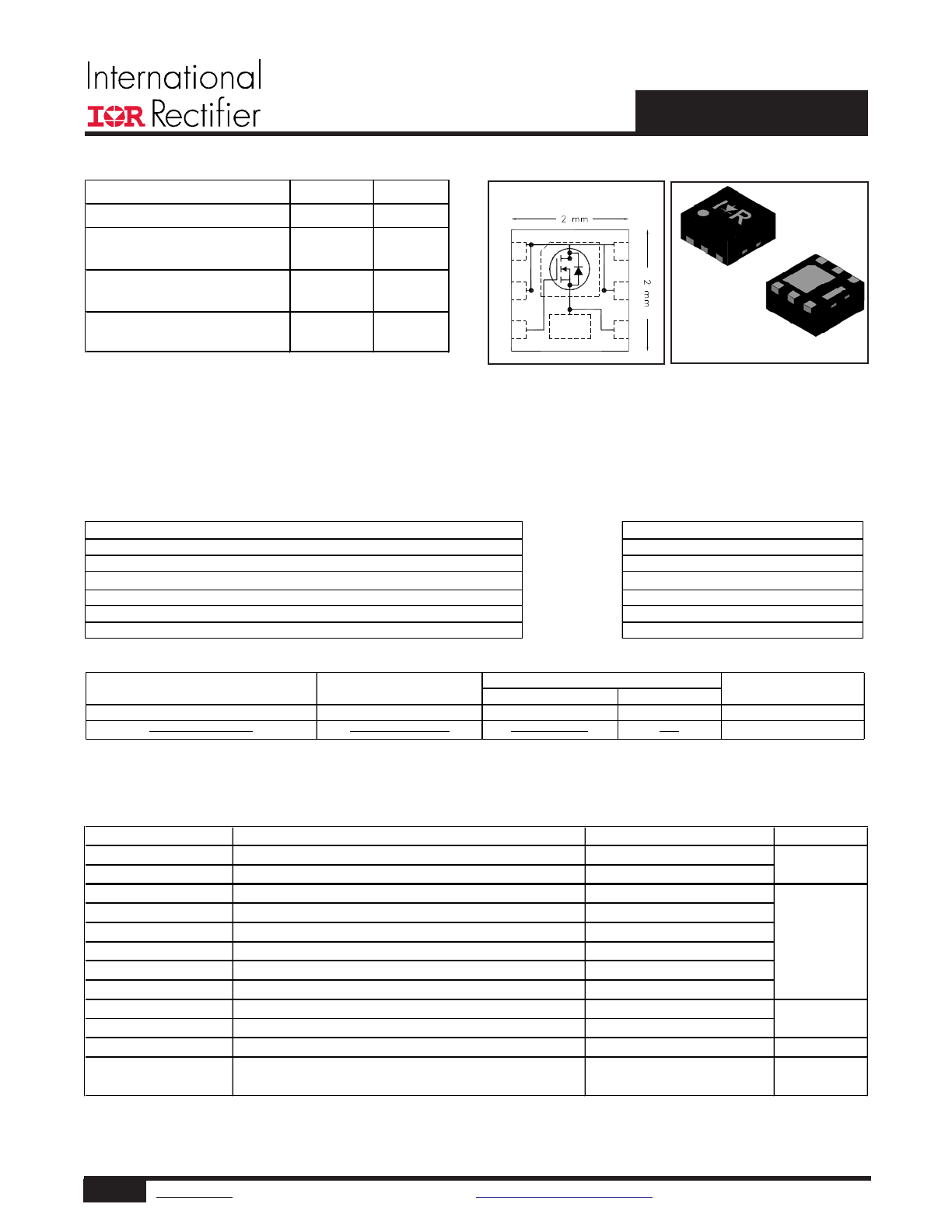
G 3
S
D 2
D 1
4 S
5 D
6 D
TOP VIEW
D
2mm x 2mm PQFN
G
D
D
S
D
D
S
D
V
DS
20
V
V
GS
±12
V
R
DS(on) max
(@V
GS
= 4.5V)
11.7
mΩ
R
DS(on) max
(@V
GS
= 2.5V)
15.5
m
Ω
I
D
(@T
C (Bottom)
= 25°C)
12
d
A
Absolute Maximum Ratings
Parameter
Units
V
DS
Drain-to-Source Voltage
V
GS
Gate-to-Source Voltage
I
D
@ T
A
= 25°C
Continuous Drain Current, V
GS
@ 4.5V
I
D
@ T
A
= 70°C
Continuous Drain Current, V
GS
@ 4.5V
I
D
@ T
C(Bottom)
= 25°C
Continuous Drain Current, V
GS
@ 4.5V
i
I
D
@ T
C(Bottom)
= 70°C
Continuous Drain Current, VGS @ 4.5V
i
I
D
@ T
C(Bottom)
= 25°C
Continuous Drain Current, V
GS
@ 4.5V (Package Limited)
I
DM
Pulsed Drain Current
c
P
D
@T
A
= 25°C
Power Dissipation
g
P
D
@T
C(Bottom)
= 25°C
Power Dissipation
g
Linear Derating Factor
g
W/°C
T
J
Operating Junction and
T
STG
Storage Temperature Range
-55 to + 150
1.98
0.016
9.6
Max.
10
18
d
88
±12
20
8.3
22
d
12
d
V
W
A
°C
IRLHS6242PbF
1
www.irf.com
©
2013 International Rectifier
Submit Datasheet Feedback
December 17, 2013
Form
Quantity
IRLHS6242TRPbF
PQFN 2mm x 2mm
Tape and Reel
4000
IRLHS6242TR2PbF
PQFN 2mm x 2mm
Tape and Reel
400
EOL notice # 259
Orderable part number
Package Type
Standard Pack
Note
Features
Resulting Benefits
Low R
DSon
(
≤ 11.7mΩ)
Lower Conduction Losses
Low Thermal Resistance to PCB (
≤ 13°C/W)
Enable better thermal dissipation
Low Profile (
≤ 1.0mm)
results in
Increased Power Density
Industry-Standard Pinout
⇒
Multi-Vendor Compatibility
Compatible with Existing Surface Mount Techniques
Easier Manufacturing
RoHS Compliant Containing no Lead, no Bromide and no Halogen
Environmentally Friendlier
MSL1, Industrial Qualification
Increased Reliability
2
www.irf.com
©
2013 International Rectifier
Submit Datasheet Feedback
December 17, 2013
IRLHS6242PbF
S
D
G
Notes:
Repetitive rating; pulse width limited by max. junction temperature.
Package is limited to 12A by die-source to lead-frame bonding technology.
Pulse width ≤ 400μs; duty cycle ≤ 2%.
When mounted on 1 ich square copper board.
R
θ
is measured at
T
J
of approximately 90°C.
For DESIGN AID ONLY, not subject to production testing.
Calculated continuous current based on maximum allowable junction temperature.
Static @ T
J
= 25°C (unless otherwise specified)
Parameter
Min. Typ. Max. Units
BV
DSS
Drain-to-Source Breakdown Voltage
20
–––
–––
V
ΔΒV
DSS
/
ΔT
J
Breakdown Voltage Temp. Coefficient
–––
6.8
–––
mV/°C
R
DS(on)
Static Drain-to-Source On-Resistance
–––
9.4
11.7
–––
12.4
15.5
V
GS(th)
Gate Threshold Voltage
0.5
0.8
1.1
V
ΔV
GS(th)
Gate Threshold Voltage Coefficient
–––
-4.2
–––
mV/°C
I
DSS
Drain-to-Source Leakage Current
–––
–––
1.0
–––
–––
150
I
GSS
Gate-to-Source Forward Leakage
–––
–––
100
Gate-to-Source Reverse Leakage
–––
–––
-100
gfs
Forward Transconductance
36
–––
–––
S
Q
g
Total Gate Charge
h
–––
14
–––
V
DS
= 10V
Q
gs
Gate-to-Source Charge
h
–––
1.5
–––
Q
gd
Gate-to-Drain Charge
h
–––
6.3
–––
R
G
Gate Resistance
–––
2.1
–––
Ω
t
d(on)
Turn-On Delay Time
–––
5.8
–––
t
r
Rise Time
–––
15
–––
t
d(off)
Turn-Off Delay Time
–––
19
–––
t
f
Fall Time
–––
13
–––
C
iss
Input Capacitance
–––
1110
–––
C
oss
Output Capacitance
–––
260
–––
C
rss
Reverse Transfer Capacitance
–––
180
–––
Diode Characteristics
Parameter
Min. Typ. Max. Units
I
S
Continuous Source Current
(Body Diode)
I
SM
Pulsed Source Current
(Body Diode)
c
V
SD
Diode Forward Voltage
–––
–––
1.2
V
t
rr
Reverse Recovery Time
–––
15
23
ns
Q
rr
Reverse Recovery Charge
–––
12
18
nC
t
on
Forward Turn-On Time
Time is dominated by parasitic Inductance
MOSFET symbol
nA
ns
A
pF
nC
V
GS
= 4.5V
V
GS
= 12V
V
GS
= -12V
–––
–––
88
–––
–––
22
Conditions
V
GS
= 0V, I
D
= 250μA
Reference to 25°C, I
D
= 1mA
V
GS
= 4.5V, I
D
= 8.5A
ed
Conditions
See Fig.15
ƒ = 1.0MHz
T
J
= 25°C, I
F
= 8.5A
d, V
DD
= 10V
di/dt = 210A/μs
e
T
J
= 25°C, I
S
= 8.5A
d, V
GS
= 0V
e
showing the
integral reverse
p-n junction diode.
R
G
=1.8
Ω
V
DS
= 10V, I
D
= 8.5A
d
V
DS
= 16V, V
GS
= 0V, T
J
= 125°C
μA
I
D
= 8.5A
d (See Fig.17 & 18)
ID = 8.5A
d
V
GS
= 0V
V
DS
= 10V
V
DS
= 16V, V
GS
= 0V
V
DS
= V
GS
, I
D
= 10μA
V
GS
= 2.5V, I
D
= 8.5A
ed
m
Ω
V
DD
= 10V, V
GS
= 4.5V
e
Thermal Resistance
Parameter
Typ.
Max.
Units
R
θJC
(Bottom)
Junction-to-Case
g
–––
13
R
θJC
(Top)
Junction-to-Case
g
–––
94
°C/W
R
θJA
Junction-to-Ambient
f
–––
63
R
θJA
(<10s)
Junction-to-Ambient
f
–––
46
3
www.irf.com
©
2013 International Rectifier
Submit Datasheet Feedback
December 17, 2013
IRLHS6242PbF
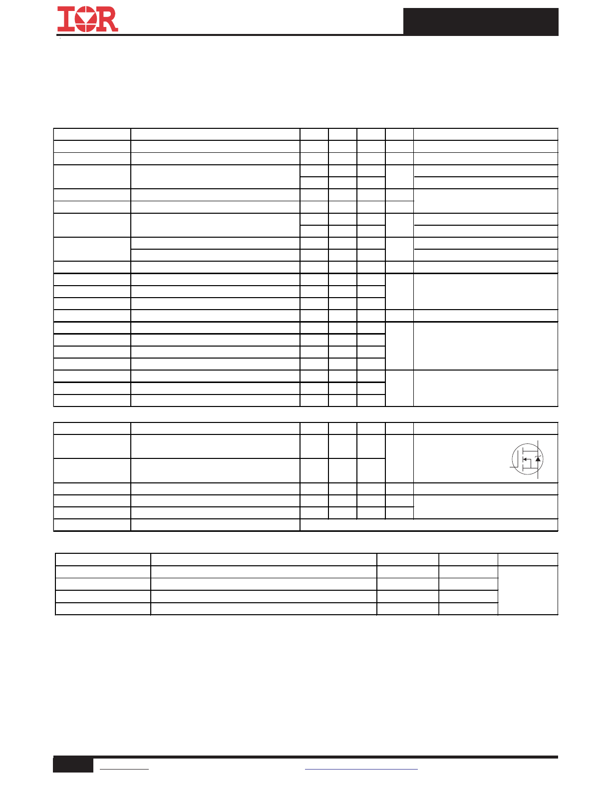
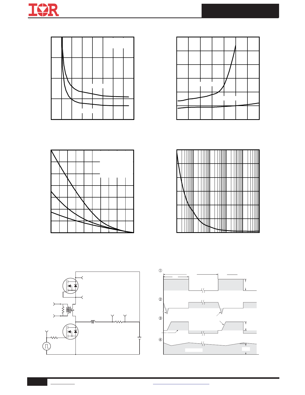
Fig 4. Normalized On-Resistance vs. Temperature
Fig 2. Typical Output Characteristics
Fig 1. Typical Output Characteristics
Fig 3. Typical Transfer Characteristics
Fig 6. Typical Gate Charge vs.Gate-to-Source Voltage
Fig 5. Typical Capacitance vs.Drain-to-Source Voltage
0.1
1
10
100
VDS, Drain-to-Source Voltage (V)
1
10
100
I D
, D
ra
in
-t
o-
S
ou
rc
e
C
ur
re
nt
(
A
)
1.4V
≤60μs PULSE WIDTH
Tj = 150°C
VGS
TOP
10V
4.5V
3.0V
2.5V
2.0V
1.8V
1.5V
BOTTOM
1.4V
1.0
1.5
2.0
2.5
3.0
3.5
VGS, Gate-to-Source Voltage (V)
1.0
10
100
I D
, D
ra
in
-t
o-
S
ou
rc
e
C
ur
re
nt
(
A
)
TJ = 25°C
TJ = 150°C
VDS = 10V
≤60μs PULSE WIDTH
-60 -40 -20 0 20 40 60 80 100 120 140 160
TJ , Junction Temperature (°C)
0.6
0.8
1.0
1.2
1.4
1.6
R
D
S
(o
n)
,
D
ra
in
-t
o-
S
ou
rc
e
O
n
R
es
is
ta
nc
e
(
N
or
m
al
iz
ed
)
ID = 8.5A
VGS = 4.5V
1
10
100
VDS, Drain-to-Source Voltage (V)
100
1000
10000
C
, C
ap
ac
ita
nc
e
(p
F
)
VGS = 0V, f = 1 MHZ
Ciss = Cgs + Cgd, C ds SHORTED
Crss = Cgd
Coss = Cds + Cgd
Coss
Crss
Ciss
0
5
10
15
20
25
30
35
QG, Total Gate Charge (nC)
0.0
2.0
4.0
6.0
8.0
10.0
12.0
14.0
V
G
S
, G
at
e-
to
-S
ou
rc
e
V
ol
ta
ge
(
V
)
VDS= 16V
VDS= 10V
VDS= 4.0V
ID= 8.5A
0.1
1
10
100
VDS, Drain-to-Source Voltage (V)
0.01
0.1
1
10
100
I D
, D
ra
in
-t
o-
S
ou
rc
e
C
ur
re
nt
(
A
)
VGS
TOP
10V
4.5V
3.0V
2.5V
2.0V
1.8V
1.5V
BOTTOM
1.4V
≤60μs PULSE WIDTH
Tj = 25°C
1.4V
4
www.irf.com
©
2013 International Rectifier
Submit Datasheet Feedback
December 17, 2013
IRLHS6242PbF
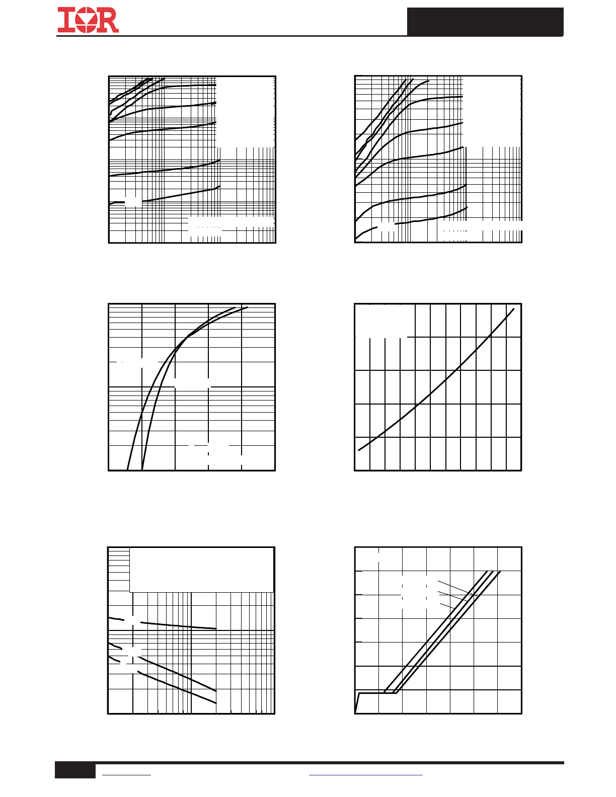
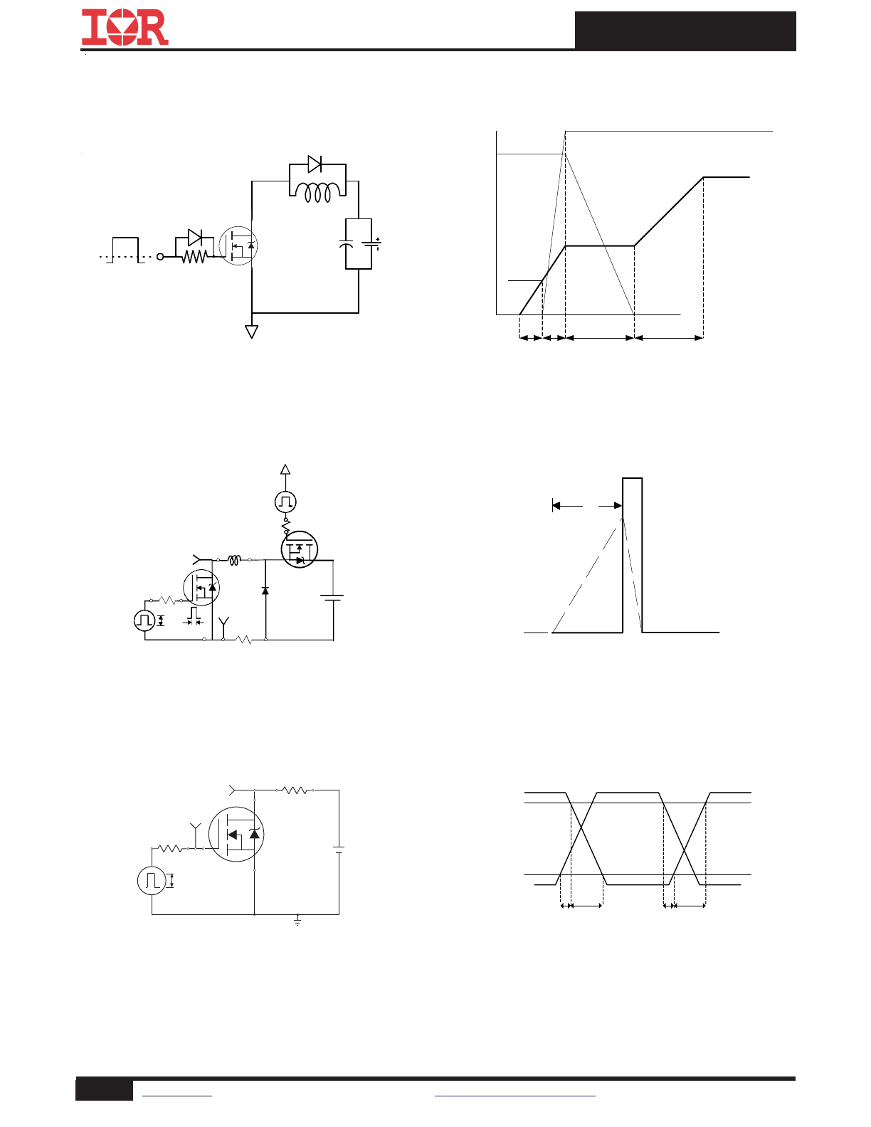
Fig 11. Maximum Effective Transient Thermal Impedance, Junction-to-Case (Bottom)
Fig 8. Maximum Safe Operating Area
Fig 9. Maximum Drain Current vs.
Case (Bottom) Temperature
Fig 7. Typical Source-Drain Diode Forward Voltage
Fig 10. Threshold Voltage vs. Temperature
1E-006
1E-005
0.0001
0.001
0.01
0.1
1
t1 , Rectangular Pulse Duration (sec)
0.01
0.1
1
10
100
T
he
rm
al
R
es
po
ns
e
(
Z
th
JC
)
°
C
/W
0.20
0.10
D = 0.50
0.02
0.01
0.05
SINGLE PULSE
( THERMAL RESPONSE )
Notes:
1. Duty Factor D = t1/t2
2. Peak Tj = P dm x Zthjc + Tc
-75 -50 -25
0
25
50
75 100 125 150
TJ , Temperature ( °C )
0.2
0.4
0.6
0.8
1.0
1.2
1.4
1.6
V
G
S
(t
h)
, G
at
e
th
re
sh
ol
d
V
ol
ta
ge
(
V
)
ID = 25μA
ID = 250μA
ID = 1.0mA
ID = 1.0A
25
50
75
100
125
150
TC , Case Temperature (°C)
0
5
10
15
20
25
I D
,
D
ra
in
C
ur
re
nt
(
A
)
Limited By Package
0
1
10
100
VDS, Drain-to-Source Voltage (V)
0.1
1
10
100
1000
I D
,
D
ra
in
-t
o-
S
ou
rc
e
C
ur
re
nt
(
A
)
OPERATION IN THIS AREA
LIMITED BY R DS(on)
Tc = 25°C
Tj = 150°C
Single Pulse
100μsec
1msec
10msec
DC
Limited by
Wire Bond
0.4
0.5
0.6
0.7
0.8
0.9
1.0
1.1
VSD, Source-to-Drain Voltage (V)
1.0
10
100
I S
D
, R
ev
er
se
D
ra
in
C
ur
re
nt
(
A
)
TJ = 25°C
TJ = 150°C
VGS = 0V
5
www.irf.com
©
2013 International Rectifier
Submit Datasheet Feedback
December 17, 2013
IRLHS6242PbF
Fig 13. Typical On-Resistance vs. Drain Current
Fig 12. On-Resistance vs. Gate Voltage
Fig 15. Typical Power vs. Time
Fig 14. Maximum Avalanche Energy vs. Drain Current
Fig 16.
Peak Diode Recovery dv/dt Test Circuit for N-Channel
HEXFET
®
Power MOSFETs
Circuit Layout Considerations
• Low Stray Inductance
• Ground Plane
• Low Leakage Inductance
Current Transformer
P.W.
Period
di/dt
Diode Recovery
dv/dt
Ripple
≤ 5%
Body Diode Forward Drop
Re-Applied
Voltage
Reverse
Recovery
Current
Body Diode Forward
Current
V
GS
=10V
V
DD
I
SD
Driver Gate Drive
D.U.T. I
SD
Waveform
D.U.T. V
DS
Waveform
Inductor Curent
D =
P.W.
Period
*
V
GS
= 5V for Logic Level Devices
*
+
-
+
+
+
-
-
-
R
G
V
DD
• dv/dt controlled by R
G
• Driver same type as D.U.T.
• I
SD
controlled by Duty Factor "D"
• D.U.T. - Device Under Test
D.U.T
25
50
75
100
125
150
Starting TJ , Junction Temperature (°C)
0
10
20
30
40
50
60
70
E
A
S
,
S
in
gl
e
P
ul
se
A
va
la
nc
he
E
ne
rg
y
(m
J)
ID
TOP 2.2A
4.3A
BOTTOM 8.5A
1E-5
1E-4
1E-3
1E-2
1E-1
1E+0
Time (sec)
0
100
200
300
400
500
600
S
in
gl
e
P
ul
se
P
ow
er
(
W
)
0
2
4
6
8
10
12
14
16
VGS, Gate -to -Source Voltage (V)
5
10
15
20
25
R
D
S
(o
n)
,
D
ra
in
-t
o
-S
ou
rc
e
O
n
R
es
is
ta
nc
e
(m
Ω
)
ID = 8.5A
TJ = 125°C
TJ = 25°C
0
10
20
30
40
50
60
70
ID, Drain Current (A)
5
10
15
20
25
30
35
R
D
S
(o
n)
,
D
ra
in
-t
o
-S
ou
rc
e
O
n
R
es
is
ta
nc
e
(m
Ω
)
Vgs = 2.5V
Vgs = 4.5V
6
www.irf.com
©
2013 International Rectifier
Submit Datasheet Feedback
December 17, 2013
IRLHS6242PbF
Fig 18b. Unclamped Inductive Waveforms
Fig 18a. Unclamped Inductive Test Circuit
tp
V
(BR)DSS
I
AS
RG
IAS
0.01
Ω
tp
D.U.T
L
VDS
+
- VDD
DRIVER
A
15V
20V
Fig 19a. Switching Time Test Circuit
Fig 19b. Switching Time Waveforms
V
GS
V
DS
90%
10%
t
d(on)
t
d(off)
t
r
t
f
Fig 17a. Gate Charge Test Circuit
Fig 17b. Gate Charge Waveform
Vds
Vgs
Id
Vgs(th)
Qgs1 Qgs2
Qgd
Qgodr
1K
VCC
DUT
0
L
S
V
DS
Pulse Width ≤ 1 µs
Duty Factor ≤ 0.1
R
D
V
GS
R
G
D.U.T.
10V
+
-
V
DD
V
GS
7
www.irf.com
©
2013 International Rectifier
Submit Datasheet Feedback
December 17, 2013
IRLHS6242PbF
PQFN 2x2 Outline Package Details
For footprint and stencil design recommendations, please refer to application note AN-1154 at
http://www.irf.com/technical-info/appnotes/an-1154.pdf
Note: For the most current drawing please refer to IR website at:
http://www.irf.com/package/
PQFN 2x2 Outline Part Marking
8
www.irf.com
©
2013 International Rectifier
Submit Datasheet Feedback
December 17, 2013
IRLHS6242PbF
PQFN 2x2 Outline Tape and Reel
9
www.irf.com
©
2013 International Rectifier
Submit Datasheet Feedback
December 17, 2013
IRLHS6242PbF
Qualification standards can be found at International Rectifier’s web site
http://www.irf.com/product-info/reliability
Applicable version of JEDEC standard at the time of product release.
IR WORLD HEADQUARTERS: 101 N. Sepulveda Blvd., El Segundo, California 90245, USA
To contact International Rectifier, please visit
http://www.irf.com/whoto-call/
MS L1
(per JEDEC J-S TD-020D
††
)
RoHS compliant
Yes
PQFN 2mm x 2mm
Qualification information
†
Moisture Sensitivity Level
Qualification level
Industrial
†
(per JEDEC JES D47F
††
guidelines )
Date
Comments
• Updated ordering information to reflect the End-Of-life (EOL) of the mini-reel option (EOL notice #259)
• Updated Qual level from "Consumer" to "Industrial" on page 1, 9
• Updated data sheet with new IR corporate template
Revision History
12/17/2013