
HEXFET
®
Power MOSFET
Notes
through
are on page 11
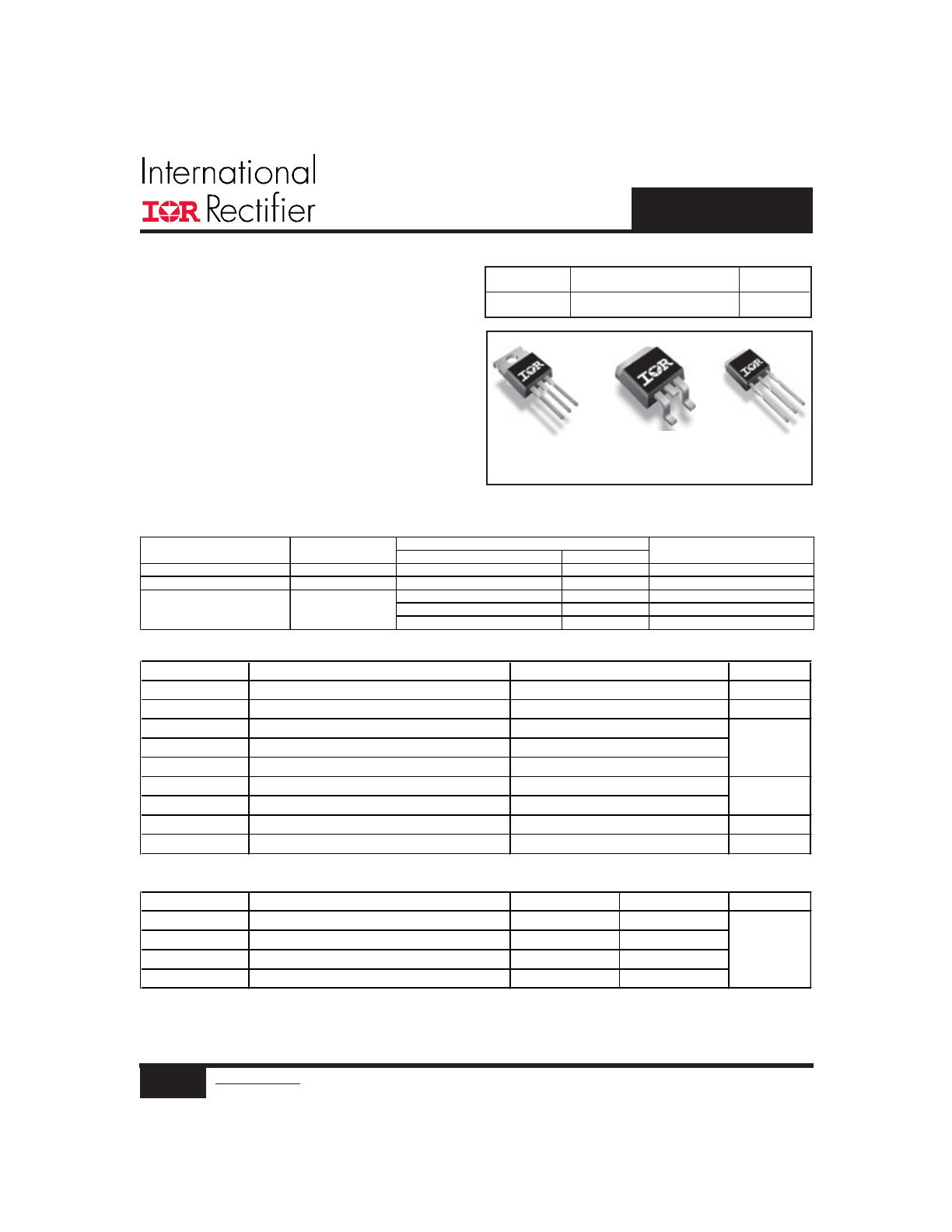
D
2
Pak
IRL3713SPbF
TO-220AB
IRL3713PbF
TO-262
IRL3713LPbF
Applications
Benefits
l
Ultra-Low Gate Impedance
l
Very Low R
DS(on)
at 4.5V V
GS
l
Fully Characterized Avalanche Voltage
and Current
l
Lead-Free
l
High Frequency Isolated DC-DC
Converters with Synchronous Rectification
for Telecom and Industrial Use
l
High Frequency Buck Converters for Computer
Processor Powe
r
l
100% R
G
Tested
V
DSS
R
DS(on)
max (m
W)
I
D
30V
3.0@V
GS
= 10V
260A
* R
θJC
(end of life) for D
2
Pak and TO-262 = 0.50°C/W. This is the maximum measured value after 1000 temperature
cycles from -55 to 150°C and is accounted for by the physical wearout of the die attach medium.
Symbol
Parameter
Units
V
DS
Drain-Source Voltage
V
V
GS
Gate-to-Source Voltage
V
I
D
@ T
C
= 25°C
Continuous Drain Current, V
GS
@ 10V
I
D
@ T
C
= 100°C Continuous Drain Current, V
GS
@ 10V
A
I
DM
Pulsed Drain Current
c
P
D
@T
C
= 25°C
Maximum Power Dissipation
P
D
@Tc = 100°C Maximum Power Dissipation
Linear Derating Factor
W/°C
T
J
, T
STG
Junction and Storage Temperature Range
°C
Symbol
Parameter
Typ
Max
Units
R
θJC
Junction-to-Case
i
–––
0.45*
R
qCS
Case-to-Sink, Flat, Greased Surface
f
0.50
–––
R
θJA
Junction-to-Ambient
fi
–––
62
R
θJA
Junction-to-Ambient (PCB Mount)
gi
–––
40
Thermal Resistance
Absolute Maximum Ratings
Max
260
h
180
h
1040
h
30
± 20
2.2
170
°C/W
W
-55 to +175
330
SMPS MOSFET
IRL3713SPbF
1
www.irf.com
©
2013 International Rectifier June 21, 2013
Base Part Number
Form
Quantity
IRL3713PbF
TO-220
Tube
50
IRL3713PbF
IRL3713SLPbF
TO-262
Tube
50
IRL3713SLPbF
Tube
50
IRL3713SPbF
Tape and Reel Left
800
IRL3713STRLPbF
Tape and Reel Right
800
IRL3713STRRPbF
Package Type
Standard Pack
Orderable Part Number
IRL3713SPbF
D
2
Pak
2
www.irf.com
©
2013 International Rectifier June 21, 2013
IRL3713/S/LPbF
Symbol
Parameter
Min
Typ Max Units
V
(BR)DSS
Drain-to-Source Breakdown Voltage
30
–––
–––
V
ΔV
(BR)DSS
/
ΔT
J
Breakdown Voltage Temp. Coefficient
–––
0.027
–––
V/°C
–––
2.6
3.0
–––
3.3
4.0
V
GS(th)
Gate Threshold Voltage
1.0
–––
2.5
V
–––
–––
50
–––
–––
20
–––
–––
100
Gate-to-Source Forward Leakage
–––
–––
200
Gate-to-Source Reverse Leakage
–––
–––
-200
Symbol
Parameter
Min
Typ Max Units
gfs
Forward Transconductance
76
–––
–––
S
Q
g
Total Gate Charge
–––
75
110
Q
gs
Gate-to-Source Charge
–––
24
–––
nC
Q
gd
Gate-to-Drain ("Miller") Charge
–––
37
–––
Q
OSS
Output Gate Charge
61
92
R
G
Gate Resistance
0.5
–––
3.4
Ω
t
d(on)
Turn-On Delay Time
–––
16
–––
t
r
Rise Time
–––
160
–––
t
d(off)
Turn-Off Delay Time
–––
40
–––
t
f
Fall Time
–––
57
–––
C
iss
Input Capacitance
–––
5890
–––
C
oss
Output Capacitance
–––
3130
–––
C
rss
Reverse Transfer Capacitance
–––
630
–––
Symbol
Parameter
Units
E
AS
mJ
I
AR
A
Symbol
Parameter
Min
Typ Max Units
Continuous Source Current
(Body Diode)
Pulsed Source Current
(Body Diode)
ch
–––
0.80
1.3
–––
0.68
–––
t
rr
Reverse Recovery Time
–––
75
110
ns
Q
rr
Reverse Recovery Charge
–––
140
210
nC
t
rr
Reverse Recovery Time
–––
78
120
ns
Q
rr
Reverse Recovery Charge
–––
160
240
nC
T
J
= 125°C, I
F
= 30A, V
R
= 20V
di/dt = 100A/μs
e
T
J
= 125°C, I
S
= 30A, V
GS
= 0V
e
T
J
= 25°C, I
F
= 30A, V
R
= 0V
di/dt = 100A/μs
e
Conditions
integral reverse
p-n junction diode.
T
J
= 25°C, I
S
= 30A, V
GS
= 0V
e
MOSFET symbol
showing the
–––
Conditions
V
DS
= 15V, I
D
= 30A
I
D
= 30A
V
DS
= 15V
V
GS
= 4.5V
e
V
GS
= 0V
V
DS
= 15V
1530
46
V
DS
= 30V, V
GS
= 0V
V
DS
= 24V, V
GS
= 0V, T
J
= 125°C
V
GS
= 20V
Conditions
V
GS
= 0V, I
D
= 250μA
Reference to 25°C, I
D
= 1mA
V
GS
= 10V, I
D
= 38A
e
V
GS
= -20V
V
GS
= 4.5V, I
D
= 30A
e
Max
V
GS
= 4.5V
f
V
DD
= 15V
I
D
= 30A
R
G
= 1.8
Ω
V
DS
= 24V, V
GS
= 0V
ƒ = 1.0MHz
V
DS
= V
GS
, I
D
= 250μA
Static @ T
J
= 25°C (unless otherwise specified)
R
DS(on)
Static Drain-to-Source On-Resistance
I
GSS
Diode Characteristics
Avalanche Characteristics
Dynamic @ T
J
= 25°C (unless otherwise specified)
m
Ω
I
DSS
Drain-to-Source Leakage Current
μA
Avalanche Current
c
Typ
–––
nA
ns
pF
Single Pulse Avalanche Energy
d
I
S
–––
––– 260
h
V
GS
= 0V, V
DS
= 15V
V
SD
Diode Forward Voltage
V
A
I
SM
–––
––– 1040
h
3
www.irf.com
©
2013 International Rectifier June 21, 2013
IRL3713/S/LPbF
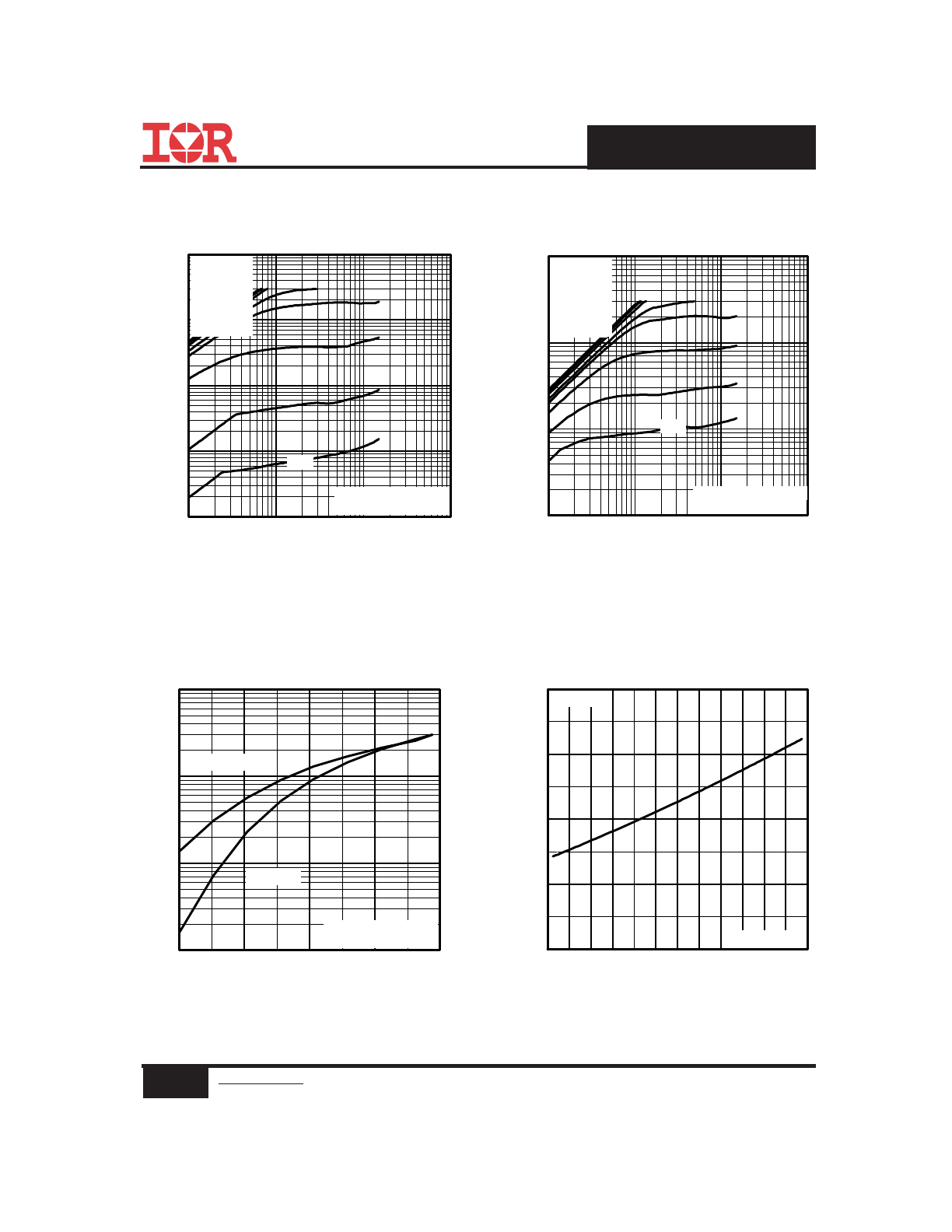
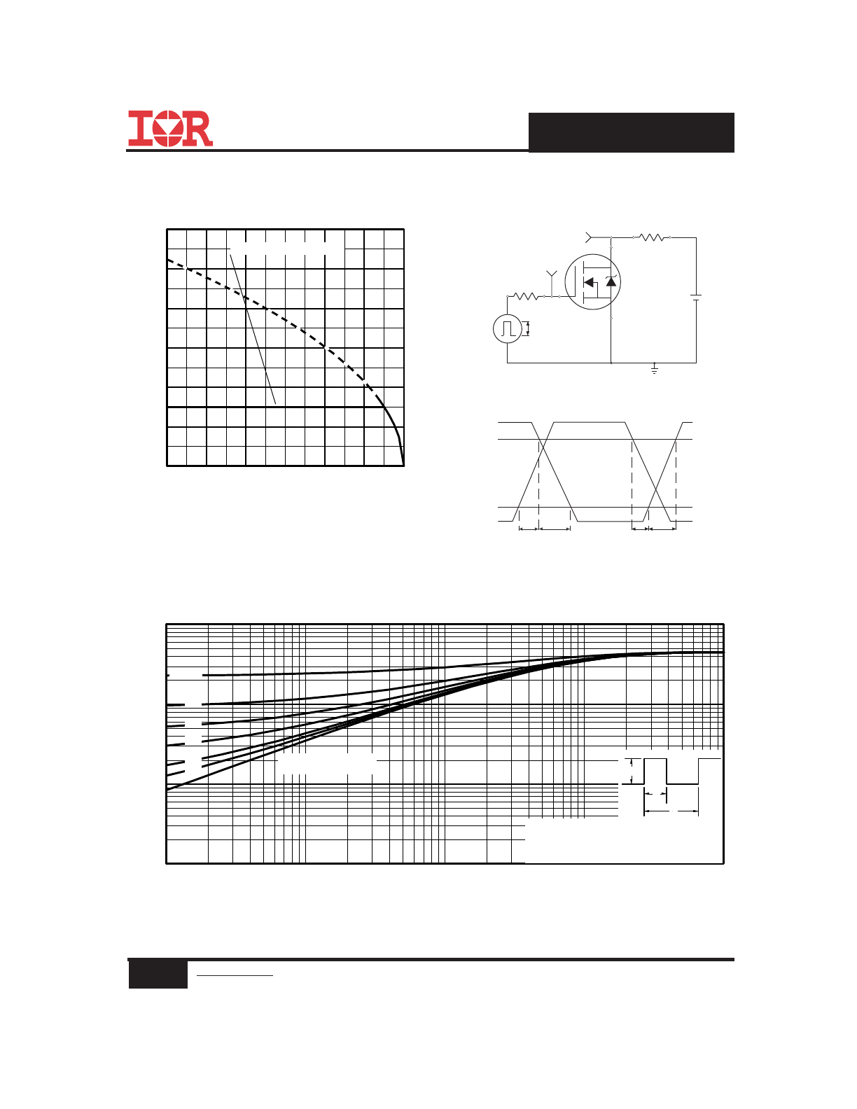
Fig 4. Normalized On-Resistance
Vs. Temperature
Fig 2. Typical Output Characteristics
Fig 1. Typical Output Characteristics
Fig 3. Typical Transfer Characteristics
0.1
1
10
100
1000
0.1
1
10
100
20μs PULSE WIDTH
T = 25 C
J
°
TOP
BOTTOM
VGS
10V
8.0V
6.0V
4.5V
4.0V
3.3V
2.8V
2.5V
V , Drain-to-Source Voltage (V)
I , Drain-to-Source Current (A)
DS
D
2.5V
1
10
100
1000
0.1
1
10
100
20μs PULSE WIDTH
T = 175 C
J
°
TOP
BOTTOM
VGS
10V
8.0V
6.0V
4.5V
4.0V
3.3V
2.8V
2.5V
V , Drain-to-Source Voltage (V)
I , Drain-to-Source Current (A)
DS
D
2.5V
1
10
100
1000
2.5
3.0
3.5
4.0
4.5
V = 15V
20μs PULSE WIDTH
DS
V , Gate-to-Source Voltage (V)
I , Drain-to-Source Current (A)
GS
D
T = 25 C
J
°
T = 175 C
J
°
-60 -40 -20 0 20 40 60 80 100 120 140 160 180
0.0
0.5
1.0
1.5
2.0
T , Junction Temperature ( C)
R , Drain-to-Source On Resistance
(Normalized)
J
D
S
(on)
°
V
=
I =
GS
D
10V
260A
4
www.irf.com
©
2013 International Rectifier June 21, 2013
IRL3713/S/LPbF
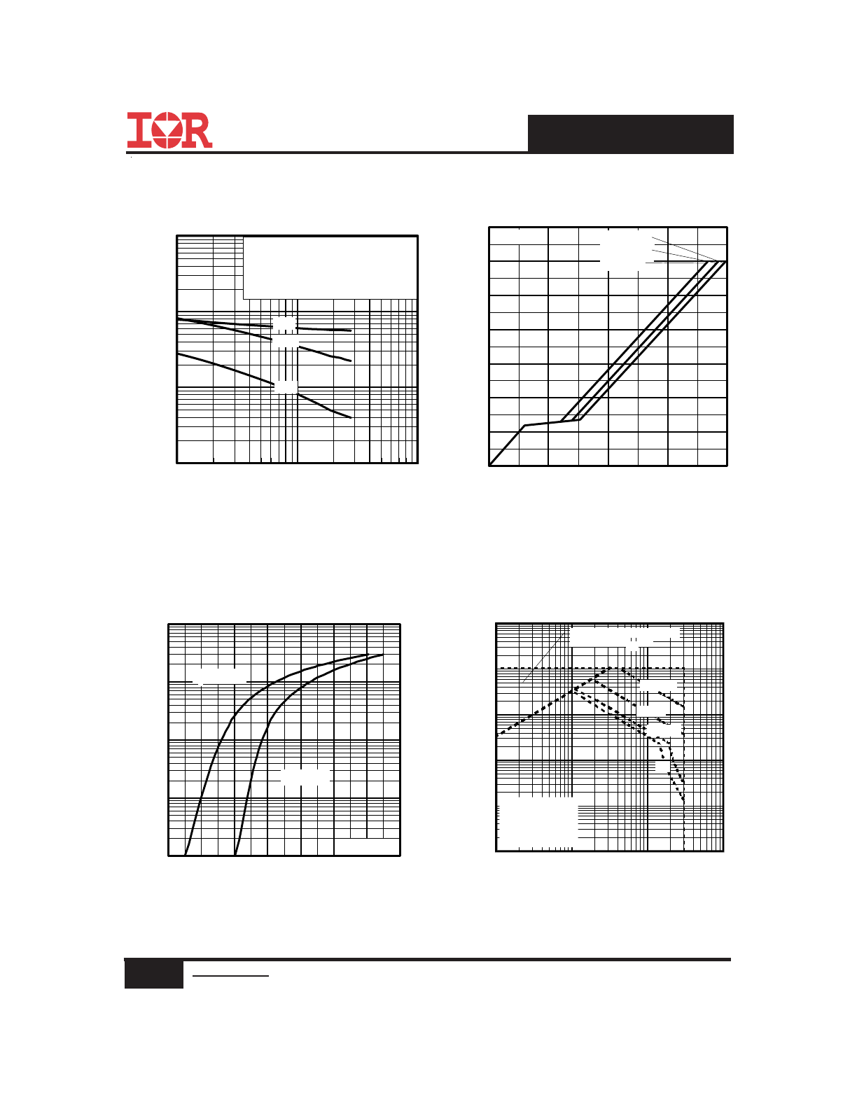
Fig 8. Maximum Safe Operating Area
Fig 6. Typical Gate Charge Vs.
Gate-to-Source Voltage
Fig 5. Typical Capacitance Vs.
Drain-to-Source Voltage
Fig 7. Typical Source-Drain Diode
Forward Voltage
0
40
80
120
160
0
2
4
6
8
10
12
14
Q , Total Gate Charge (nC)
V ,
G
at
e-t
o-Source Vol
tage (V)
G
GS
I =
D
30A
V
= 6V
DS
V
= 15V
DS
V
= 24V
DS
0.1
1
10
100
1000
0.2
0.4
0.6
0.8
1.0
1.2
1.4
1.6
V ,Source-to-Drain Voltage (V)
I , Reverse Drain Current (A)
SD
SD
V = 0 V
GS
T = 25 C
J
°
T = 175 C
J
°
1
10
100
VDS, Drain-to-Source Voltage (V)
100
1000
10000
100000
C
, C
ap
ac
ita
nc
e(
pF
)
Coss
Crss
Ciss
VGS = 0V, f = 1 MHZ
Ciss = Cgs + Cgd, Cds SHORTED
Crss = Cgd
Coss = Cds + Cgd
0.1
1
10
100
VDS, Drain-to-Source Voltage (V)
0.1
1
10
100
1000
10000
I D
,
D
ra
in
-t
o-
S
ou
rc
e
C
ur
re
nt
(
A
)
Tc = 25°C
Tj = 175°C
Single Pulse
1msec
10msec
OPERATION IN THIS AREA
LIMITED BY RDS(on)
100μsec
DC
5
www.irf.com
©
2013 International Rectifier June 21, 2013
IRL3713/S/LPbF
Fig 10a. Switching Time Test Circuit
V
DS
90%
10%
V
GS
t
d(on)
t
r
t
d(off)
t
f
Fig 10b. Switching Time Waveforms
V
DS
Pulse Width ≤ 1 µs
Duty Factor ≤ 0.1 %
R
D
V
GS
R
G
D.U.T.
10V
+
-
V
DD
Fig 11. Maximum Effective Transient Thermal Impedance, Junction-to-Case
Fig 9. Maximum Drain Current Vs.
Case Temperature
0.001
0.01
0.1
1
0.00001
0.0001
0.001
0.01
0.1
Notes:
1. Duty factor D = t / t
2. Peak T = P
x Z
+ T
1
2
J
DM
thJC
C
P
t
t
DM
1
2
t , Rectangular Pulse Duration (sec)
Ther
m
al
R
esponse
(Z
)
1
thJC
0.01
0.02
0.05
0.10
0.20
D = 0.50
SINGLE PULSE
(THERMAL RESPONSE)
25
50
75
100
125
150
175
0
50
100
150
200
250
300
T , Case Temperature ( C)
I , Drain Current (A)
°
C
D
LIMITED BY PACKAGE
6
www.irf.com
©
2013 International Rectifier June 21, 2013
IRL3713/S/LPbF
Q
G
Q
GS
Q
GD
V
G
Charge
D.U.T.
V
DS
I
D
I
G
3mA
V
GS
.3
μF
50K
Ω
.2
μF
12V
Current Regulator
Same Type as D.U.T.
Current Sampling Resistors
+
-
10 V
Fig 13b. Gate Charge Test Circuit
Fig 13a. Basic Gate Charge Waveform
Fig 12c. Maximum Avalanche Energy
Vs. Drain Current
Fig 12b. Unclamped Inductive Waveforms
Fig 12a. Unclamped Inductive Test Circuit
tp
V
(BR)DSS
I
AS
25
50
75
100
125
150
175
0
500
1000
1500
2000
2500
3000
Starting T , Junction Temperature ( C)
E
,
S
ingl
e P
ul
se A
val
anche E
ner
gy (
m
J)
J
AS
°
ID
TOP
BOTTOM
30A
38A
46A
RG
IAS
0.01
Ω
tp
D.U.T
L
VDS
+
- VDD
DRIVER
A
15V
20V
V
GS
7
www.irf.com
©
2013 International Rectifier June 21, 2013
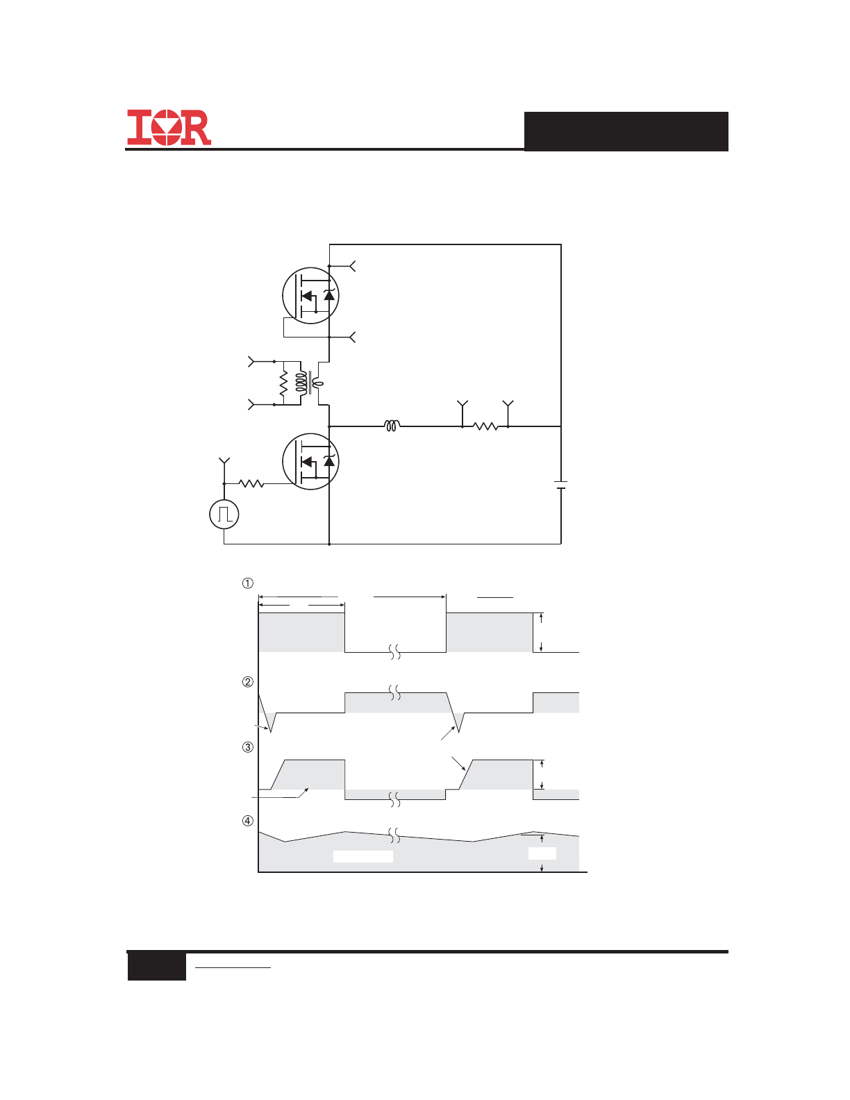
IRL3713/S/LPbF
P.W.
Period
di/dt
Diode Recovery
dv/dt
Ripple
≤ 5%
Body Diode Forward Drop
Re-Applied
Voltage
Reverse
Recovery
Current
Body Diode Forward
Current
V
GS
=10V
V
DD
I
SD
Driver Gate Drive
D.U.T. I
SD
Waveform
D.U.T. V
DS
Waveform
Inductor Curent
D =
P.W.
Period
+
-
+
+
+
-
-
-
Fig 14. For N-Channel HEXFET
®
Power MOSFETs
*
V
GS
= 5V for Logic Level Devices
Peak Diode Recovery dv/dt Test Circuit
R
G
V
DD
• dv/dt controlled by R
G
• Driver same type as D.U.T.
• I
SD
controlled by Duty Factor "D"
• D.U.T. - Device Under Test
D.U.T
Circuit Layout Considerations
• Low Stray Inductance
• Ground Plane
• Low Leakage Inductance
Current Transformer
*
8
www.irf.com
©
2013 International Rectifier June 21, 2013
IRL3713/S/LPbF
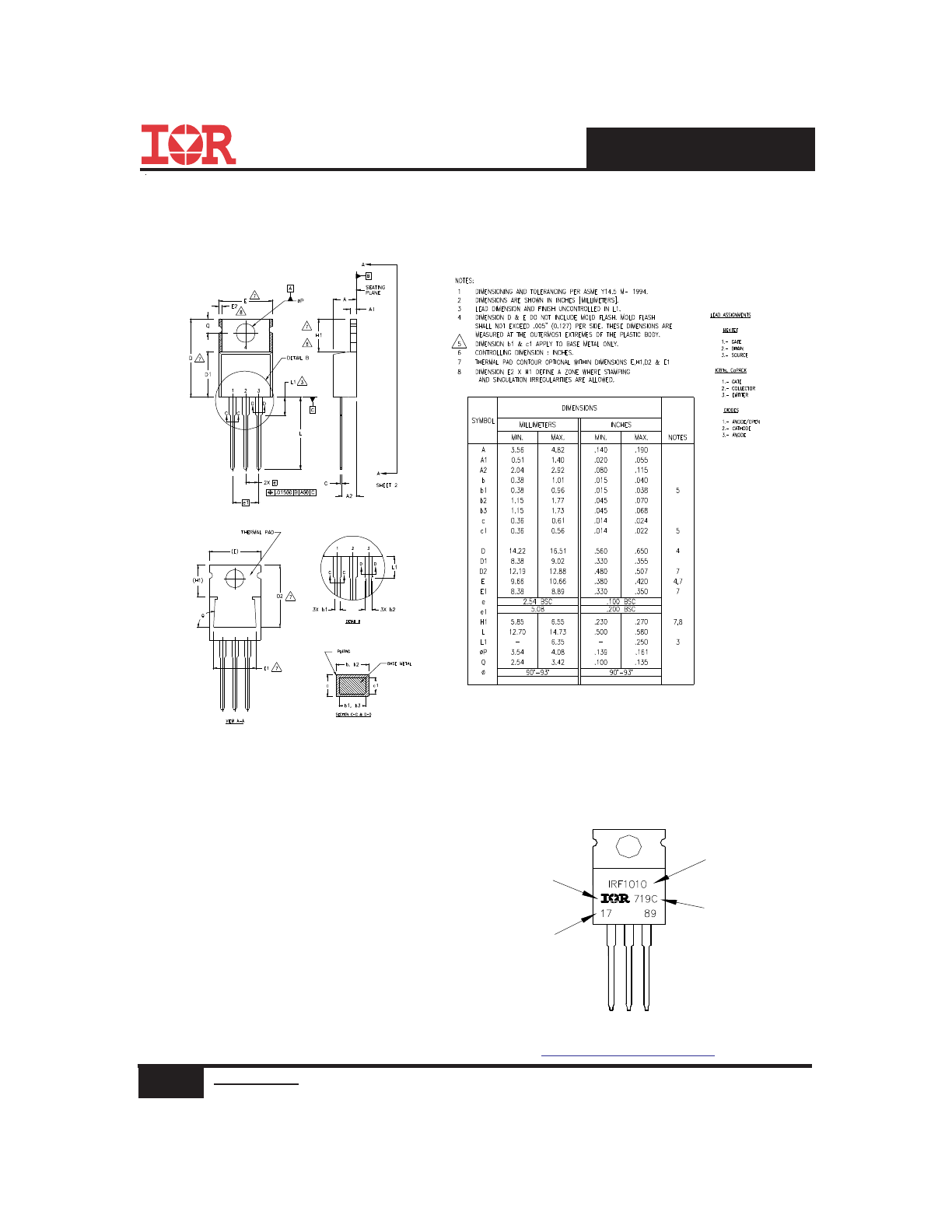
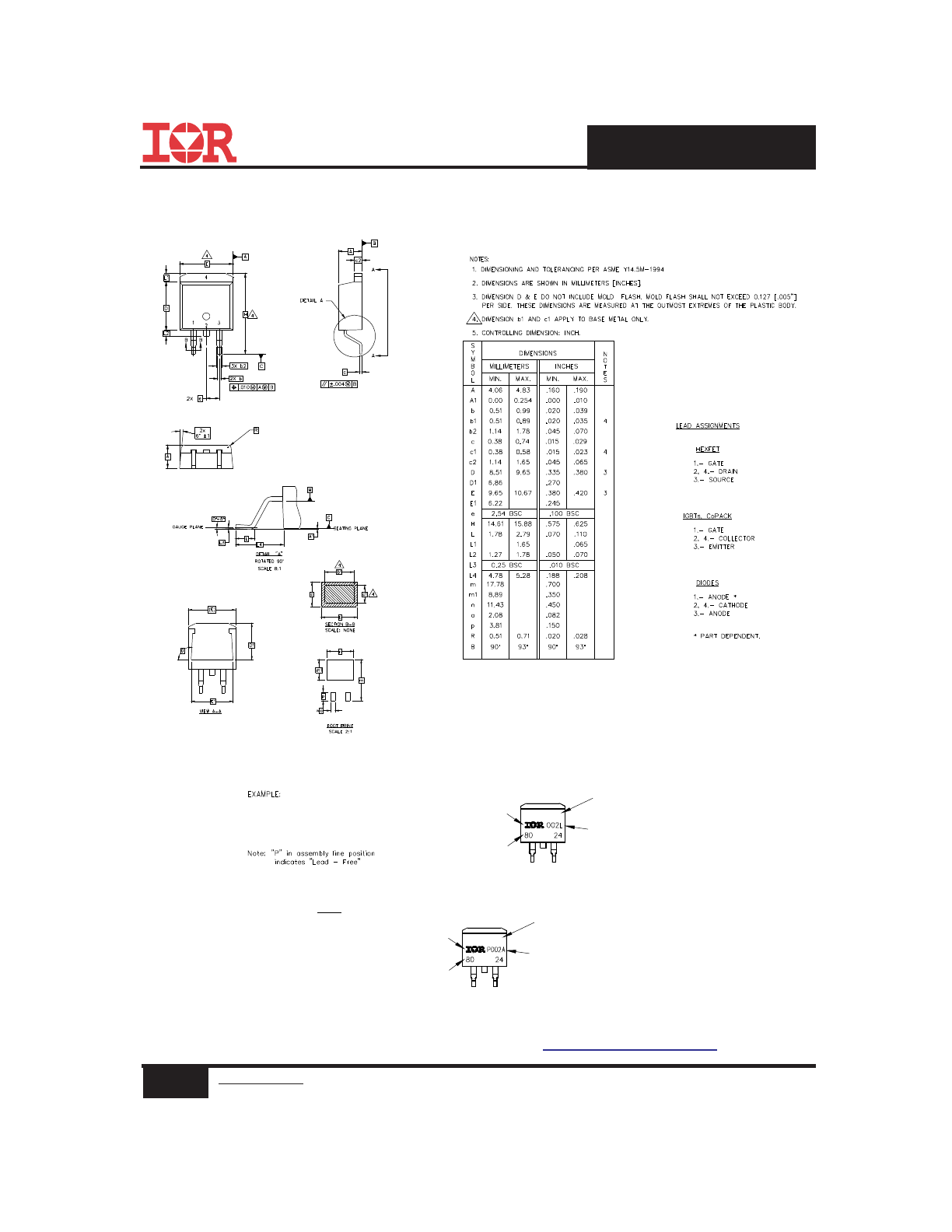
TO-220AB Part Marking Information
E XAMPLE :
IN T HE AS S E MB LY LINE "C"
T HIS IS AN IRF 1010
LOT CODE 1789
AS S E MB L ED ON WW 19, 1997
PART NU MB ER
AS S EMBL Y
L OT CODE
DAT E CODE
YE AR 7 = 1997
L INE C
WEE K 19
L OGO
R ECT IF IE R
INT E RNAT IONAL
Note: "P" in assembly line
position indicates "Lead-Free"
TO-220AB Package Outline
Dimensions are shown in millimeters (inches)
Note: For the most current drawing please refer to IR website at
http://www.irf.com/package/
9
www.irf.com
©
2013 International Rectifier June 21, 2013
IRL3713/S/LPbF
D
2
Pak Part Marking Information
D
2
Pak Package Outline
Dimensions are shown in millimeters (inches)
DAT E CODE
YE AR 0 = 2000
WEEK 02
A = AS S EMB LY S IT E CODE
RECT IF IER
INT ERNAT IONAL
PART NUMB ER
P = DES IGNAT ES LEAD - F REE
PRODU CT (OPT IONAL)
F 530S
IN T HE AS S EMB LY L INE "L"
AS S EMB L ED ON WW 02, 2000
T HIS IS AN IR F530S WIT H
L OT CODE 8024
INT ERNAT IONAL
LOGO
RECT IF IER
L OT CODE
AS S E MB L Y
YE AR 0 = 2000
PART NUMB ER
DAT E CODE
L INE L
WEE K 02
OR
F 530S
LOGO
AS S E MB L Y
L OT CODE
Note: For the most current drawing please refer to IR website at
http://www.irf.com/package/
10
www.irf.com
©
2013 International Rectifier June 21, 2013
IRL3713/S/LPbF
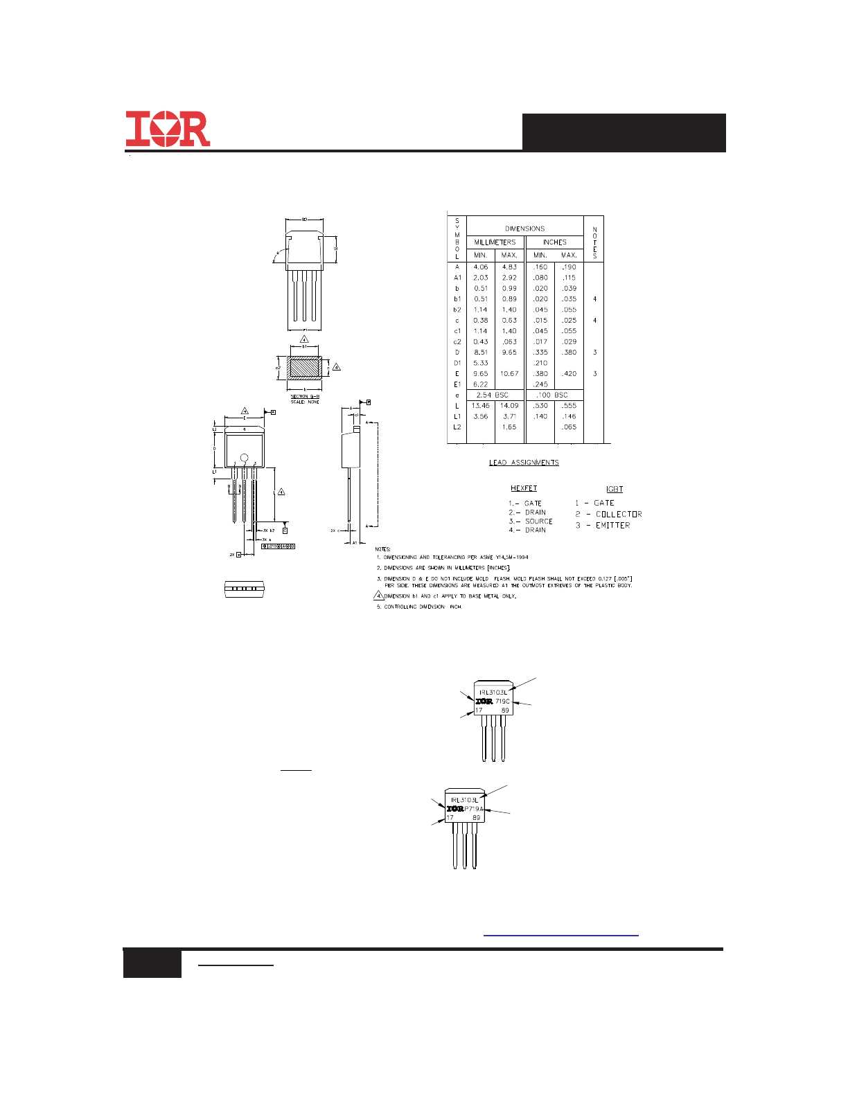
TO-262 Part Marking Information
TO-262 Package Outline
Dimensions are shown in millimeters (inches)
AS S E MB LY
L OT CODE
RE CT IF IER
INT E RNAT IONAL
AS S E MB L E D ON WW 19, 1997
Note: "P" in ass embly line
pos ition indicates "Lead-F ree"
IN T HE AS S E MB L Y LINE "C"
LOGO
T HIS IS AN IRL 3103L
L OT CODE 1789
E XAMPL E:
LINE C
DAT E CODE
WE E K 19
YE AR 7 = 1997
PART NUMB E R
PART NUMB E R
L OGO
LOT CODE
AS S E MB LY
INT E RNAT IONAL
RE CT IF IE R
PR ODU CT (OPT IONAL)
P = DE S IGNAT E S LE AD-F RE E
A = AS S E MB LY S IT E CODE
WE E K 19
YE AR 7 = 1997
DAT E CODE
OR
Note: For the most current drawing please refer to IR website at
http://www.irf.com/package/