
IRL3705NPbF
1
2018-05-25
Absolute Maximum Ratings
Symbol Parameter
Max.
Units
I
D
@ T
C
= 25°C
Continuous Drain Current, V
GS
@ 10V
89
A
I
D
@ T
C
= 100°C
Continuous Drain Current, V
GS
@ 10V
63
I
DM
Pulsed Drain Current 310
W
P
D
@T
C
= 25°C
Maximum Power Dissipation
170
Linear Derating Factor
1.1
W/°C
V
GS
Gate-to-Source Voltage
± 16
V
E
AS
Single Pulse Avalanche Energy 340
mJ
I
AR
Avalanche Current 46
A
E
AR
Repetitive Avalanche Energy 17
mJ
dv/dt
Peak Diode Recovery dv/dt 5.0
V/ns
T
J
Operating Junction and
-55 to + 175
T
STG
Storage Temperature Range
°C
Soldering Temperature, for 10 seconds (1.6mm from case)
300
Mounting torque, 6-32 or M3 screw
10 lbf•in (1.1N•m)
Thermal Resistance
Symbol Parameter
Typ.
Max.
Units
R
JC
Junction-to-Case
–––
0.90
°C/W
R
JA
Junction-to-Ambient
–––
62
R
CS
Case-to-Sink, Flat, Greased Surface
0.50
–––
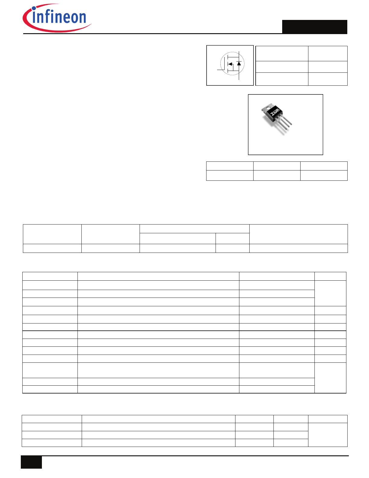
G D S
Gate Drain Source
TO-220AB
IRL3705NPbF
HEXFET
®
Power MOSFET
D
S
G
V
DSS
55V
R
DS(on)
max.
0.01
I
D
89A
Description
Fifth Generation HEXFETs utilize advanced
processing techniques to achieve extremely low on-
resistance per silicon area. This benefit, combined
with the fast switching speed and ruggedized device
design that HEXFET Power MOSFETs are well
known for, provides the designer with an extremely
efficient and reliable device for use in a wide variety
of applications.
The TO-220 package is universally preferred for all
commercial industrial applications at power
dissipation levels to approximately 50 watts. The low
thermal resistance and low package cost of the TO-
220 contribute to its wide acceptance throughout the
industry.
Logic - Level Gate Drive
Advanced Process Technology
Dynamic dv/dt Rating
175°C Operating Temperature
Fast
Switching
Fully Avalanche Rated
Lead-Free
Base part number
Package Type
Standard Pack
Orderable Part Number
Form
Quantity
IRL3705NPbF
TO-220
Tube
50
IRL3705NPbF
S
D
G
IRL3705NPbF
2
2018-05-25
Notes:
Repetitive rating; pulse width limited by max. junction temperature. (See fig.11)
V
DD
= 25V, starting T
J
= 25°C, L = 320
H, R
G
= 25
, I
AS
= 46A.(See fig.12)
I
SD
46A, di/dt 250A/µs, V
DD
V
(BR)DSS
, T
J
175°C.
Pulse width
300µs; duty cycle 2%.
Calculated continuous current based on maximum allowable junction temperature; for recommended current- handling of the
package refer to Design TIP # 93-4
.
Electrical Characteristics @ T
J
= 25°C (unless otherwise specified)
Parameter Min.
Typ.
Max.
Units
Conditions
V
(BR)DSS
Drain-to-Source Breakdown Voltage
55
–––
–––
V V
GS
= 0V, I
D
= 250µA
V
(BR)DSS
/
T
J
Breakdown Voltage Temp. Coefficient ––– 0.056 ––– V/°C Reference to 25°C, I
D
= 1mA
R
DS(on)
Static Drain-to-Source On-
Resistance
––– ––– 0.010
V
GS
= 10V, I
D
= 46A
––– ––– 0.012
V
GS
= 5.0V, I
D
= 46A
––– ––– 0.018
V
GS
= 4.0V, I
D
= 39A
V
GS(th)
Gate Threshold Voltage
1.0
–––
2.0
V V
DS
= V
GS
, I
D
= 250µA
gfs
Forward Trans conductance
50
–––
–––
S V
DS
= 25V, I
D
= 46A
I
DSS
Drain-to-Source Leakage Current
––– ––– 25
µA
V
DS
= 55V, V
GS
= 0V
––– ––– 250
V
DS
= 44V,V
GS
= 0V,T
J
=150°C
I
GSS
Gate-to-Source Forward Leakage
–––
–––
100
nA
V
GS
= 16V
Gate-to-Source Reverse Leakage
–––
––– -100
V
GS
= -16V
Q
g
Total Gate Charge
–––
–––
98
nC
I
D
= 46A
Q
gs
Gate-to-Source Charge
–––
–––
19
V
DS
= 44V
Q
gd
Gate-to-Drain Charge
–––
–––
49
V
GS
= 5.0V , See Fig. 6 and 13
t
d(on)
Turn-On Delay Time
–––
12
–––
ns
V
DD
= 28V
t
r
Rise Time
–––
140
–––
I
D
= 46A
t
d(off)
Turn-Off Delay Time
–––
37
–––
R
G
= 1.8
V
GS
= 5.0V
t
f
Fall Time
–––
78
–––
R
D
= 0.59
See Fig. 10
L
D
Internal Drain Inductance
–––
4.5
–––
Between lead,
6mm (0.25in.)
L
S
Internal Source Inductance
–––
7.5
–––
from package
and center of die contact
C
iss
Input Capacitance
––– 3600 –––
pF
V
GS
= 0V
C
oss
Output Capacitance
–––
870
–––
V
DS
= 25V
C
rss
Reverse Transfer Capacitance
–––
320
–––
ƒ = 1.0MHz, See Fig. 5
Source-Drain Ratings and Characteristics
Parameter
Min. Typ. Max. Units
Conditions
I
S
Continuous Source Current
––– ––– 89
A
MOSFET symbol
(Body Diode)
showing the
I
SM
Pulsed Source Current
––– ––– 310
integral reverse
(Body Diode)
p-n junction diode.
V
SD
Diode Forward Voltage
–––
–––
1.3
V T
J
= 25°C,I
S
= 46A,V
GS
= 0V
t
rr
Reverse Recovery Time
–––
94
140
ns T
J
= 25°C ,I
F
= 46A
Q
rr
Reverse Recovery Charge
–––
290
440
nC di/dt = 100A/µs
t
on
Forward Turn-On Time
Intrinsic turn-on time is negligible (turn-on is dominated by L
S
+L
D
)
nH
IRL3705NPbF
3
2018-05-25
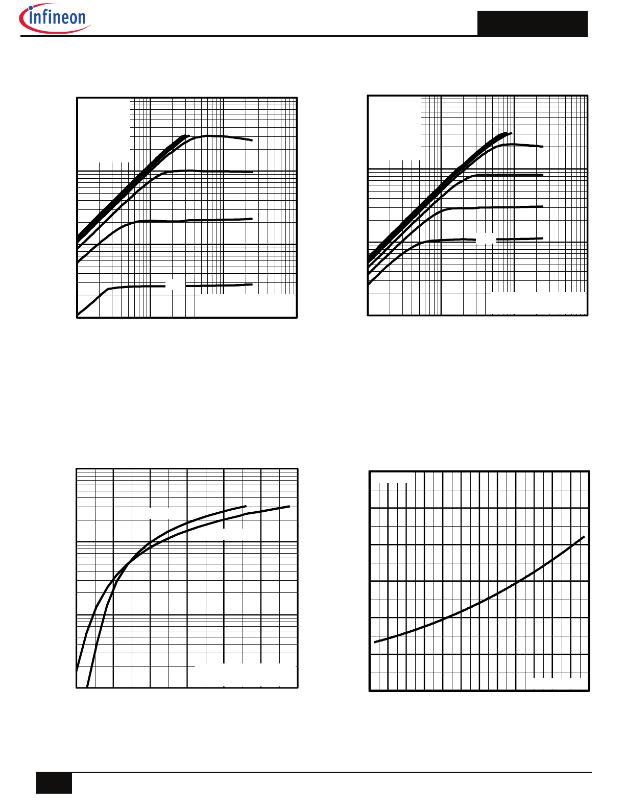
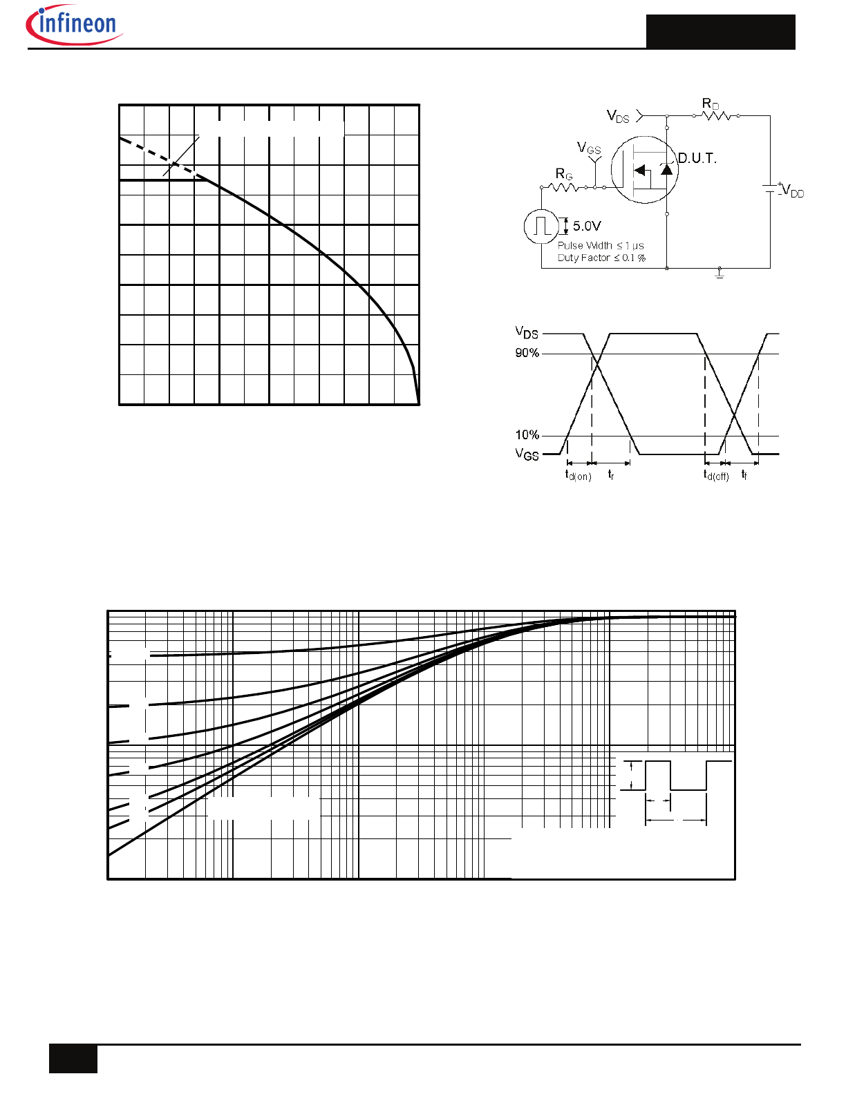
Fig. 2 Typical Output Characteristics
Fig. 3
Typical Transfer Characteristics
Fig. 4 Normalized On-Resistance
vs. Temperature
Fig. 1 Typical Output Characteristics
1
10
100
1000
0.1
1
10
100
I , Dr
ai
n-
to-
S
ourc
e
C
ur
re
nt
(
A
)
D
V , Drain-to-Source Voltage (V)
DS
A
20µs PULSE WIDTH
T = 25°C
J
VGS
TOP 15V
12V
10V
8.0V
6.0V
4.0V
3.0V
BOTTOM 2.5V
2.5V
1
10
100
1000
0.1
1
10
100
I
,
Dr
ain-
to
-Sour
ce
Cur
re
nt
(
A
)
D
V , Drain-to-Source Voltage (V)
DS
A
20µs PULSE WIDTH
T = 175°C
VGS
TOP 15V
12V
10V
8.0V
6.0V
4.0V
3.0V
BOTTOM 2.5V
2.5V
J
1
10
100
1000
2.0
3.0
4.0
5.0
6.0
7.0
8.0
T = 25°C
J
GS
V , Gate-to-Source Voltage (V)
D
I
,
Drain-t
o
-S
o
u
rce C
u
rr
e
nt (
A
)
T = 175°C
J
A
V = 25V
20µs PULSE WIDTH
DS
0.0
0.5
1.0
1.5
2.0
2.5
3.0
-60 -40 -20
0
20
40
60
80 100 120 140 160 180
J
T , Junction Temperature (°C)
R
,
Dra
in
-to
-S
ou
rce
O
n Re
si
sta
nc
e
DS
(o
n)
(N
or
m
al
ized
)
V = 10V
GS
A
I = 77A
D
IRL3705NPbF
4
2018-05-25
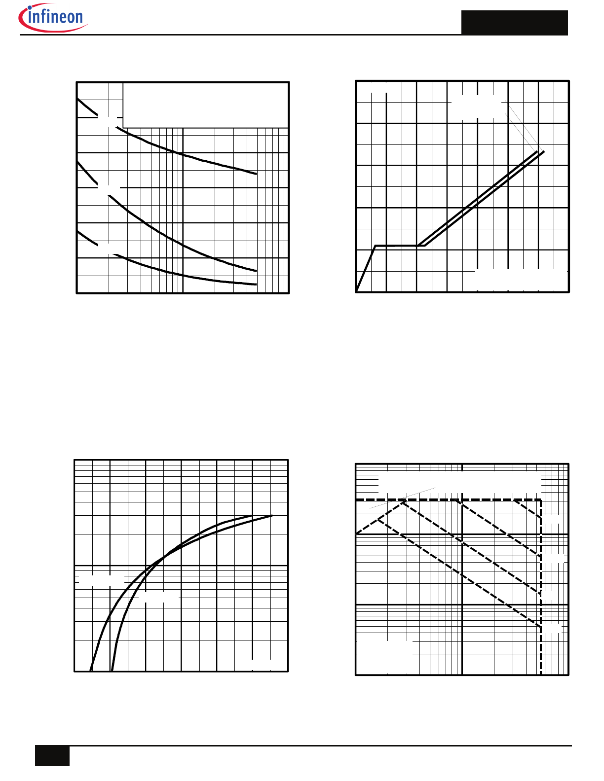
Fig 5. Typical Capacitance vs.
Drain-to-Source Voltage
Fig 8. Maximum Safe Operating Area
Fig. 7 Typical Source-to-Drain Diode
Forward Voltage
Fig 6. Typical Gate Charge vs.
Gate-to-Source Voltage
0
1000
2000
3000
4000
5000
6000
1
10
100
C
, C
apac
ita
nc
e
(p
F)
DS
V , Drain-to-Source Voltage (V)
A
V = 0V, f = 1MHz
C = C + C , C SHORTED
C = C
C = C + C
GS
iss gs gd ds
rss gd
oss ds gd
C
iss
C
oss
C
rss
0
3
6
9
12
15
0
20
40
60
80
100
120
140
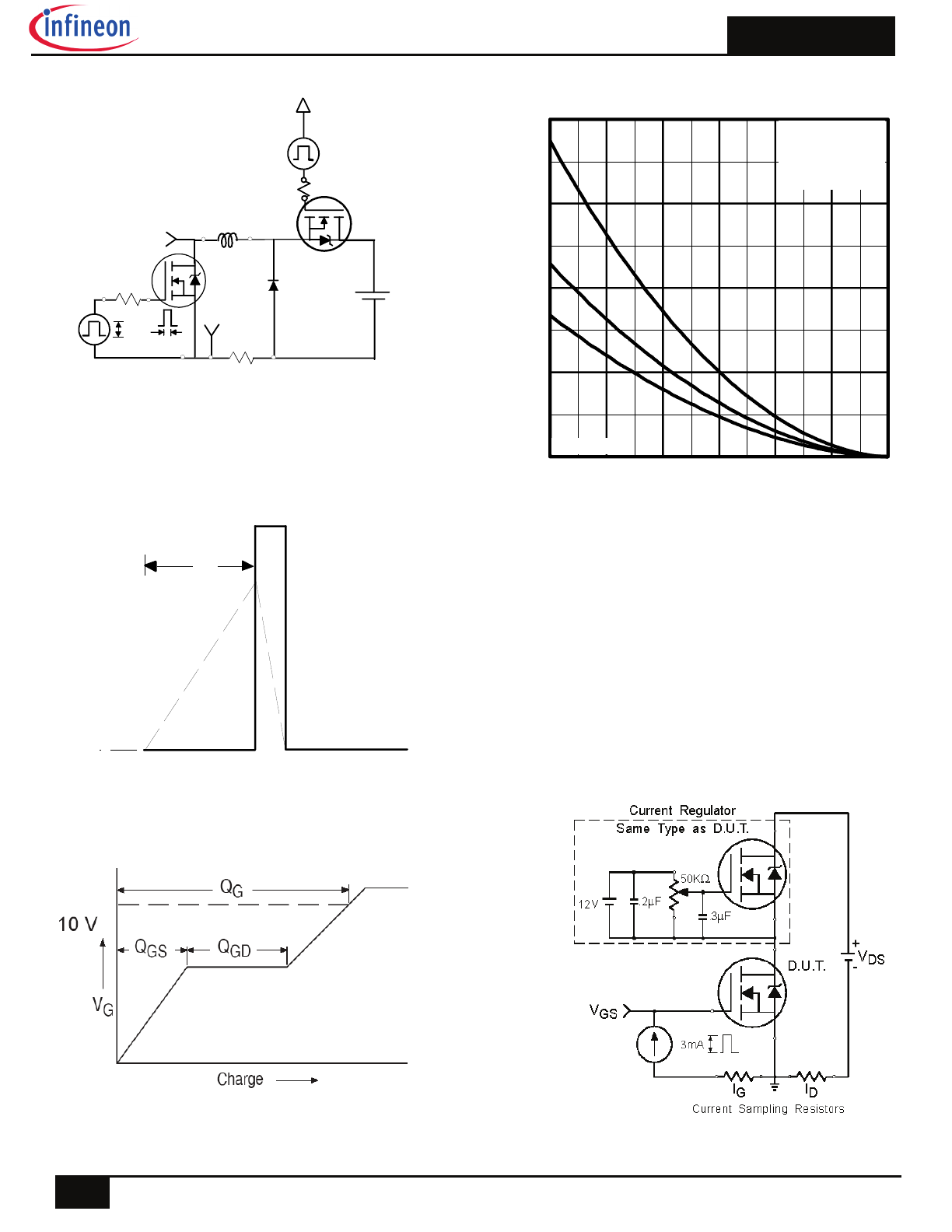
Q , Total Gate Charge (nC)
G
V
,
G
at
e-
to-
S
ourc
e V
ol
tag
e (
V
)
GS
A
FOR TEST CIRCUIT
SEE FIGURE 13
I = 46A
V = 44V
V = 28V
D
DS
DS
10
100
1000
0.4
0.8
1.2
1.6
2.0
2.4
2.8
T = 25°C
J
V = 0V
GS
V , Source-to-Drain Voltage (V)
I
,
R
ev
er
se
D
rain C
ur
rent
(
A)
SD
SD
A
T = 175°C
J
1
10
100
1000
1
10
100
V , Drain-to-Source Voltage (V)
DS
I
, Dr
ai
n Cur
re
nt
(
A
)
OPERATION IN THIS AREA LIMITED
BY R
D
DS(on)
10µs
100µs
1ms
10ms
A
T = 25°C
T = 175°C
Single Pulse
C
J
IRL3705NPbF
5
2018-05-25
Fig 11. Maximum Effective Transient Thermal Impedance, Junction-to-Case
Fig 9. Maximum Drain Current vs. Case Temperature
Fig 10a. Switching Time Test Circuit
Fig 10b. Switching Time Waveforms
25
50
75
100
125
150
175
0
20
40
60
80
100
T , Case Temperature ( C)
I
, D
ra
in
C
ur
re
nt
(
A
)
°
C
D
LIMITED BY PACKAGE
0.01
0.1
1
0.00001
0.0001
0.001
0.01
0.1
1
Notes:
1. Duty factor D = t / t
2. Peak T = P
x Z
+ T
1
2
J
DM
thJC
C
P
t
t
DM
1
2
t , Rectangular Pulse Duration (sec)
Th
e
rm
a
l R
e
spon
se
(Z
)
1
th
JC
0.01
0.02
0.05
0.10
0.20
D = 0.50
SINGLE PULSE
(THERMAL RESPONSE)
IRL3705NPbF
6
2018-05-25
Fig 12c. Maximum Avalanche Energy
vs. Drain Current
Fig 12a. Unclamped Inductive Test Circuit
Fig 12b. Unclamped Inductive Waveforms
Fig 13b. Gate Charge Test Circuit
Fig 13a. Gate Charge Waveform
0
200
400
600
800
25
50
75
100
125
150
175
J
E
,
S
ingle Pul
se
Aval
an
ch
e E
ne
rg
y (
m
J)
AS
A
Starting T , Junction Temperature (°C)
V = 25V
I
TOP 19A
33A
BOTTOM 46A
DD
D
RG
I
AS
0.01
tp
D.U.T
L
VDS
+
- VDD
DRIVER
A
15V
10V
tp
V
(BR)DSS
I
AS
IRL3705NPbF
7
2018-05-25
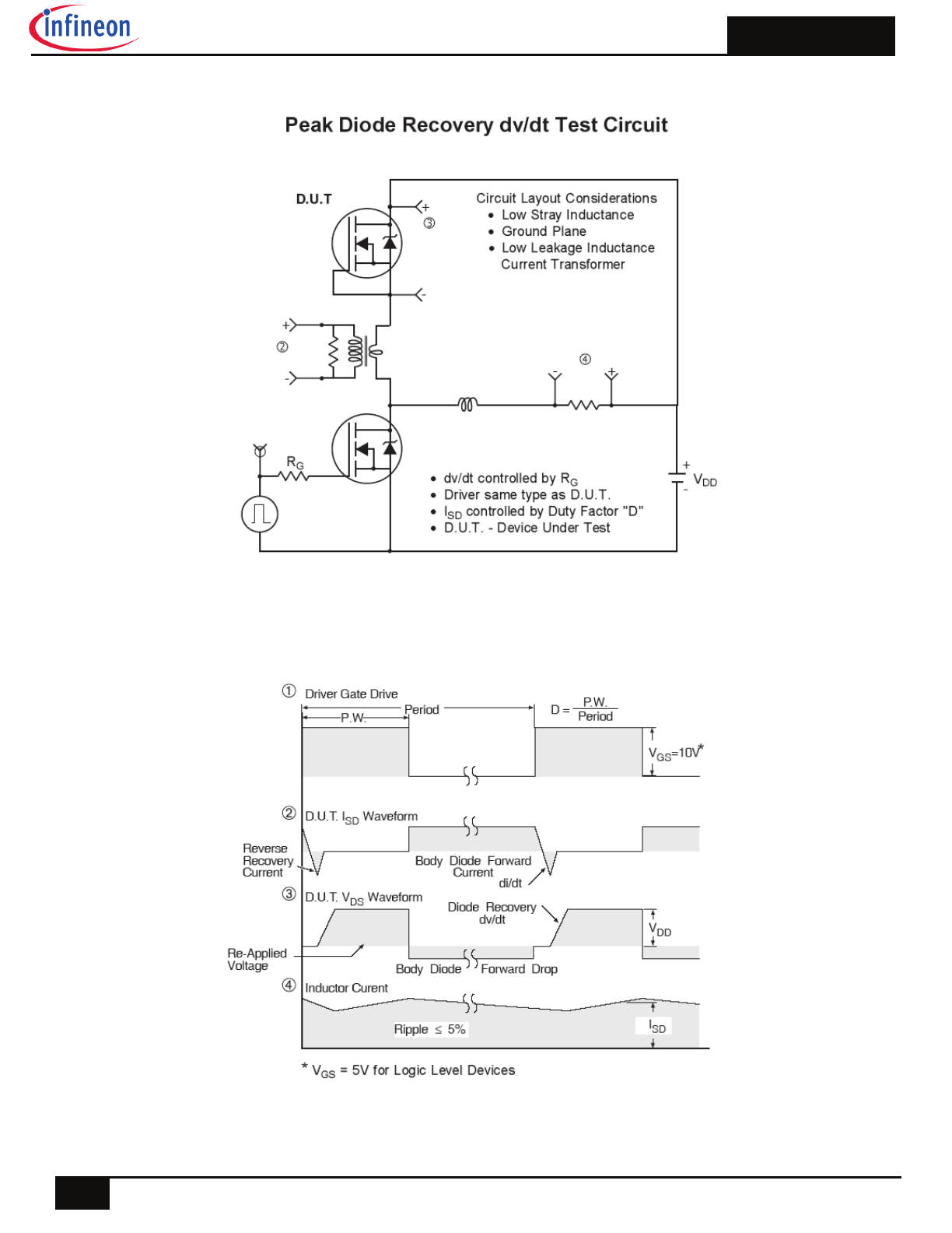
Fig 14. Peak Diode Recovery dv/dt Test Circuit for N-Channel HEXFET® Power MOSFETs
IRL3705NPbF
8
2018-05-25
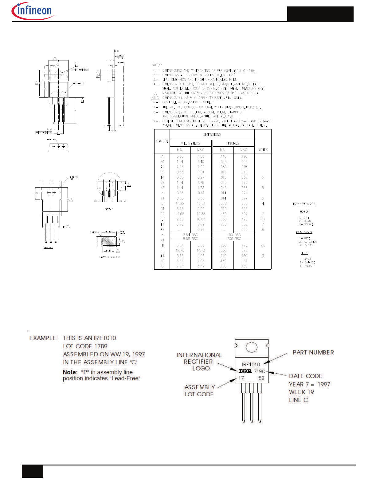
TO-220 Package Outline (Dimensions are shown in millimeters (inches)
TO-220 Part Marking Information
TO-220AB packages are not recommended for Surface Mount Application
.
IRL3705NPbF
9
2018-05-25
Revision History
Date Comments
05/25/2018
Changed datasheet with Infineon logo - all pages.
Corrected TO-220 Package outline on page 8.
Added disclaimer on last page.
Trademarks of Infineon Technologies AG
µHVIC™, µIPM™, µPFC™, AU-ConvertIR™, AURIX™, C166™, CanPAK™, CIPOS™, CIPURSE™, CoolDP™, CoolGaN™, COOLiR™, CoolMOS™, CoolSET™, CoolSiC™,
DAVE™, DI-POL™, DirectFET™, DrBlade™, EasyPIM™, EconoBRIDGE™, EconoDUAL™, EconoPACK™, EconoPIM™, EiceDRIVER™, eupec™, FCOS™,
GaNpowIR™, HEXFET™, HITFET™, HybridPACK™, iMOTION™, IRAM™, ISOFACE™, IsoPACK™, LEDrivIR™, LITIX™, MIPAQ™, ModSTACK™, my-d™, NovalithIC™,
OPTIGA™, OptiMOS™, ORIGA™, PowIRaudio™, PowIRStage™, PrimePACK™, PrimeSTACK™, PROFET™, PRO-SIL™, RASIC™, REAL3™, SmartLEWIS™, SOLID
FLASH™, SPOC™, StrongIRFET™, SupIRBuck™, TEMPFET™, TRENCHSTOP™, TriCore™, UHVIC™, XHP™, XMC™
Trademarks updated November 2015
Other Trademarks
All referenced product or service names and trademarks are the property of their respective owners.
Edition 2016-04-19
Published by
Infineon Technologies AG
81726 Munich, Germany
© 2016 Infineon Technologies AG.
All Rights Reserved.
Do you have a question about this
document?
Email:
erratum@infineon.com
Document reference
ifx1
IMPORTANT NOTICE
The information given in this document shall in no
event be regarded as a guarantee of conditions or
characteristics (“Beschaffenheitsgarantie”) .
With respect to any examples, hints or any typical
values stated herein and/or any information
regarding the application of the product, Infineon
Technologies hereby disclaims any and all
warranties and liabilities of any kind, including
without limitation warranties of non-infringement
of intellectual property rights of any third party.
In addition, any information given in this
document is subject to customer’s compliance
with its obligations stated in this document and
any applicable legal requirements, norms and
standards concerning customer’s products and
any use of the product of Infineon Technologies in
customer’s applications.
The data contained in this document is exclusively
intended for technically trained staff. It is the
responsibility of customer’s technical
departments to evaluate the suitability of the
product for the intended application and the
completeness of the product information given in
this document with respect to such application.
For further information on the product, technology,
delivery terms and conditions and prices please
contact your nearest Infineon Technologies office
(
www.infineon.com
).
Please note that this product is not qualified
according to the AEC Q100 or AEC Q101 documents
of the Automotive Electronics Council.
WARNINGS
Due to technical requirements products may
contain dangerous substances. For information on
the types in question please contact your nearest
Infineon Technologies office.
Except as otherwise explicitly approved by Infineon
Technologies in a written document signed by
authorized representatives of Infineon
Technologies, Infineon Technologies’ products
may not be used in any applications where a failure
of the product or any consequences of the use
thereof can reasonably be expected to result in
personal injury.
Qualification Information
Qualification Level
Industrial
(per JEDEC JESD47F)
†
Moisture Sensitivity Level
TO-220
N/A
RoHS Compliant
Yes
† Applicable version of JEDEC standard at the time of product release.