
INSULATED GATE BIPOLAR TRANSISTOR WITH
ULTRAFAST SOFT RECOVERY DIODE
IRGS4064DPbF
1
www.irf.com
02/16/12
V
CES
= 600V
I
C
= 10A, T
C
= 100°C
t
sc
> 5µs, T
jmax
= 175°C
V
CE(on) typ.
= 1.6V
PD - 96424
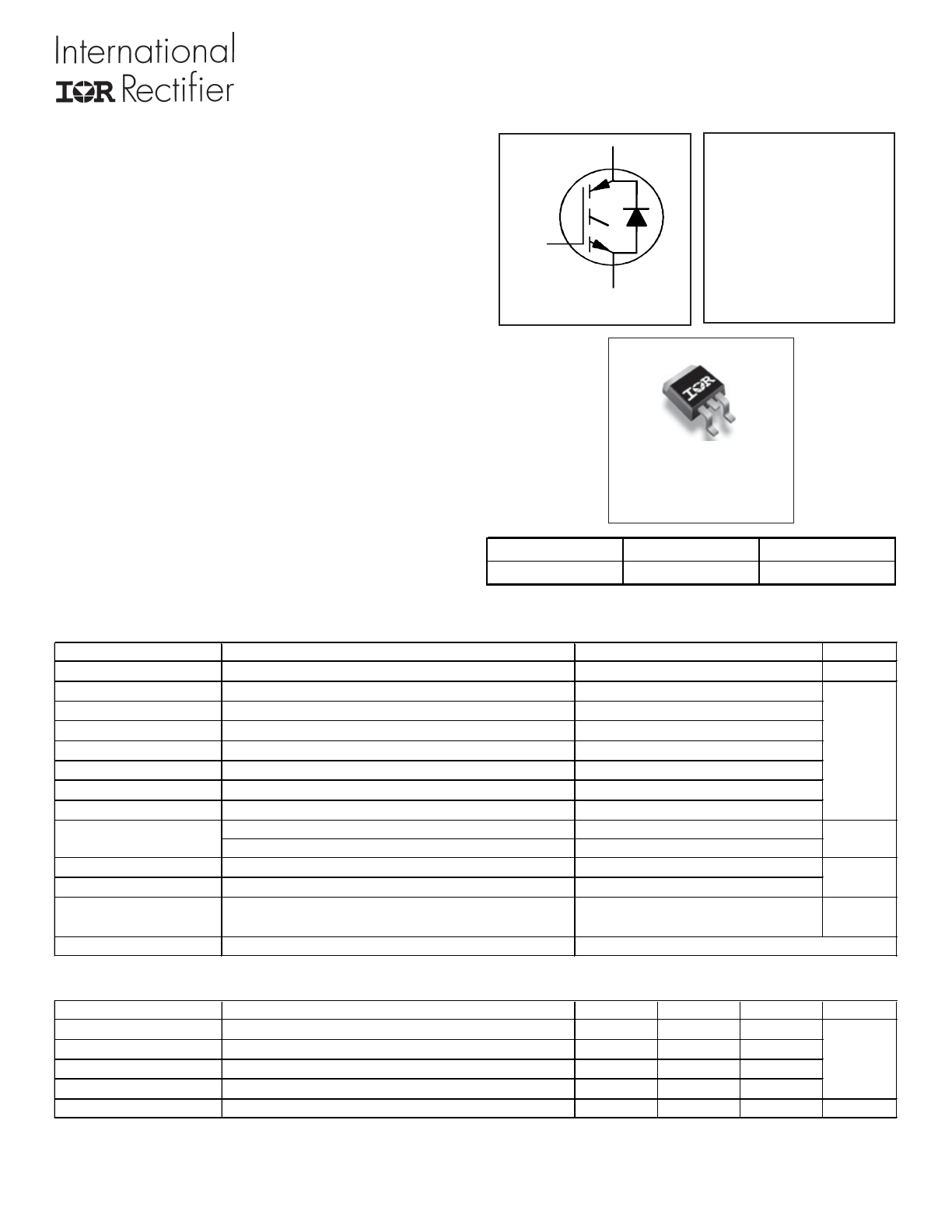
G
C
E
Gate
Collector
Emitter
E
G
n-channel
C
Features
•
Low V
CE (on)
Trench IGBT Technology
•
Low Switching Losses
•
Maximum Junction temperature 175 °C
•
5μs SCSOA
•
Square RBSOA
•
100% of The Parts Tested for (I
LM
)
•
Positive V
CE (on)
Temperature Coefficient.
•
Ultra Fast Soft Recovery Co-pak Diode
•
Tighter Distribution of Parameters
•
Lead-Free Package
Benefits
•
High Efficiency in a Wide Range of Applications
•
Suitable for a Wide Range of Switching Frequencies due
to Low V
CE (ON)
and Low Switching Losses
•
Rugged Transient Performance for Increased Reliability
•
Excellent Current Sharing in Parallel Operation
•
Low EMI
D
2
Pak
C
E
C
G
Absolute Maximum Ratings
Parameter
Max.
Units
V
CES
Collector-to-Emitter Breakdown Voltage
600
V
I
C
@ T
C
= 25°C
Continuous Collector Current
20
I
C
@ T
C
= 100°C
Continuous Collector Current
10
I
CM
Pulsed Collector Current
40
I
LM
Clamped Inductive Load Current
c
40
A
I
F
@T
C
=25°C
Diode Continuous Forward Current
20
I
F
@T
C
=100°C
Diode Continuous Forward Current
10
I
FM
Diode Maximum Forward Current
d
40
Continuous Gate-to-Emitter Voltage
±20
V
Transient Gate-to-Emitter Voltage
±30
P
D
@ T
C
=25°
Maximum Power Dissipation
101
W
P
D
@ T
C
=100°
Maximum Power Dissipation
50
T
J
Operating Junction and
°C
T
STG
Storage Temperature Range
Soldering Temperature, for 10 seconds
Thermal Resistance
Parameter
Min.
Typ.
Max. Units
R
θJC
Junction-to-Case - IGBT
e
–––
–––
1.49
R
θJC
Junction-to-Case - Diode
e
–––
–––
3.66
R
θCS
Case-to-Sink, flat, greased surface
–––
0.50
–––
R
θJA
Junction-to-Ambient, typical socket mount
e
–––
–––
40
Wt
Weight
1.5
g
°C/W
V
GE
-55 to + 175
300 (0.063 in. (1.6mm) from case)
IRGS4064DPbF
2
www.irf.com
Notes:
V
CC
= 80% (V
CES
), V
GE
= 15V, L = 28 μH, R
G
= 22
Ω.
Pulse width limited by max. junction temperature.
R
θ
is measured at T
J
approximately 90°C
Refer to AN-1086 for guidelines for measuring V
(BR)CES
safely
Maximum limits are based on statistical sample size characterization
Electrical Characteristics @ T
J
= 25°C (unless otherwise specified)
Parameter
Min. Typ.
Max.
Units Conditions
Ref.Fig
V
(BR)CES
Collector-to-Emitter Breakdown Voltage
600
—
—
V
V
GE
= 0V, I
C
= 100μA
f
ΔV
(BR)CES
/
ΔT
J
Temperature Coeff. of Breakdown Voltage
—
0.47
—
V/°C
V
GE
= 0V, I
C
= 500μA (25°C-175°C)
—
1.6
1.91
I
C
= 10A, V
GE
= 15V, T
J
= 25°C
V
CE(on)
Collector-to-Emitter Saturation Voltage
—
1.9
—
V
I
C
= 10A, V
GE
= 15V, T
J
= 150°C
5,6,7,9,
—
2.0
—
I
C
= 10A, V
GE
= 15V, T
J
= 175°C
10 ,11
V
GE(th)
Gate Threshold Voltage
4.0
—
6.5
V
V
CE
= V
GE
, I
C
= 275μA
ΔV
GE(th)
/
ΔTJ
Threshold Voltage temp. coefficient
—
-11
—
mV/°C V
CE
= V
GE
, I
C
= 1.0mA (25°C - 175°C)
gfe
Forward Transconductance
—
6.9
—
S
V
CE
= 50V, I
C
= 10A, PW = 80μs
I
CES
Collector-to-Emitter Leakage Current
—
—
25
μA
V
GE
= 0V, V
CE
= 600V
—
328
—
V
GE
= 0V, V
CE
= 600V, T
J
= 175°C
8
V
FM
Diode Forward Voltage Drop
—
2.5
3.1
V
I
F
= 10A
—
1.7
—
I
F
= 10A, T
J
= 175°C
I
GES
Gate-to-Emitter Leakage Current
—
—
±100
nA
V
GE
= ±20V
Switching Characteristics @ T
J
= 25°C (unless otherwise specified)
Parameter
Min. Typ.
Max.g Units
R ef .F ig
Q
g
Total Gate Charge (turn-on)
—
21
32
I
C
= 10A
24
Q
ge
Gate-to-Emitter Charge (turn-on)
—
5.3
8.0
nC
V
GE
= 15V
CT 1
Q
gc
Gate-to-Collector Charge (turn-on)
—
8.9
13
V
CC
= 400V
E
on
Turn-On Switching Loss
—
29
40
I
C
= 10A, V
CC
= 400V, V
GE
= 15V
E
off
Turn-Off Switching Loss
—
200
281
μJ
R
G
= 22
Ω, L = 1.0mH, T
J
= 25°C
CT 4
E
total
Total Switching Loss
—
229
313
E nergy los s es include tail & diode revers e recovery
t
d(on)
Turn-On delay time
—
27
37
I
C
= 10A, V
CC
= 400V, V
GE
= 15V
t
r
Rise time
—
15
23
ns
R
G
= 22
Ω, L = 1.0mH, T
J
= 25°C
CT 4
t
d(off)
Turn-Off delay time
—
79
90
t
f
Fall time
—
21
29
E
on
Turn-On Switching Loss
—
99
—
I
C
= 10A, V
CC
= 400V, V
GE
= 15V
13,15
E
off
Turn-Off Switching Loss
—
316
—
μJ
R
G
=22
Ω, L=1.0mH, T
J
= 175°C
f
CT 4
E
total
Total Switching Loss
—
415
—
E nergy los s es include tail & diode revers e recovery
WF 1,WF 2
t
d(on)
Turn-On delay time
—
27
—
I
C
= 10A, V
CC
= 400V, V
GE
= 15V
14,16
t
r
Rise time
—
16
—
ns
R
G
= 22
Ω, L = 1.0mH, T
J
= 175°C
CT 4
t
d(off)
Turn-Off delay time
—
98
—
WF 1,WF 2
t
f
Fall time
—
33
—
C
ies
Input Capacitance
—
594
—
pF
V
GE
= 0V
22
C
oes
Output Capacitance
—
49
—
V
CC
= 30V
C
res
Reverse Transfer Capacitance
—
17
—
f = 1.0Mhz
T
J
= 175°C, I
C
= 40A
4
RBSOA
Reverse Bias Safe Operating Area
FULL SQUARE
V
CC
= 480V, Vp =600V
CT 2
Rg = 22
Ω, V
GE
= +15V to 0V
SCSOA
Short Circuit Safe Operating Area
5
—
—
μs
V
CC
= 400V, Vp =600V
22, CT 3
Rg = 22
Ω, V
GE
= +15V to 0V
WF 4
Erec
Reverse Recovery Energy of the Diode
—
191
—
μJ
T
J
= 175°C
17,18,19
t
rr
Diode Reverse Recovery Time
—
62
—
ns
V
CC
= 400V, I
F
= 10A
20,21
I
rr
Peak Reverse Recovery Current
—
16
—
A
V
GE
= 15V, Rg = 22
Ω, L=1.0mH
WF 3
CT 6
9,10,11,12
Conditions
IRGS4064DPbF
www.irf.com
3
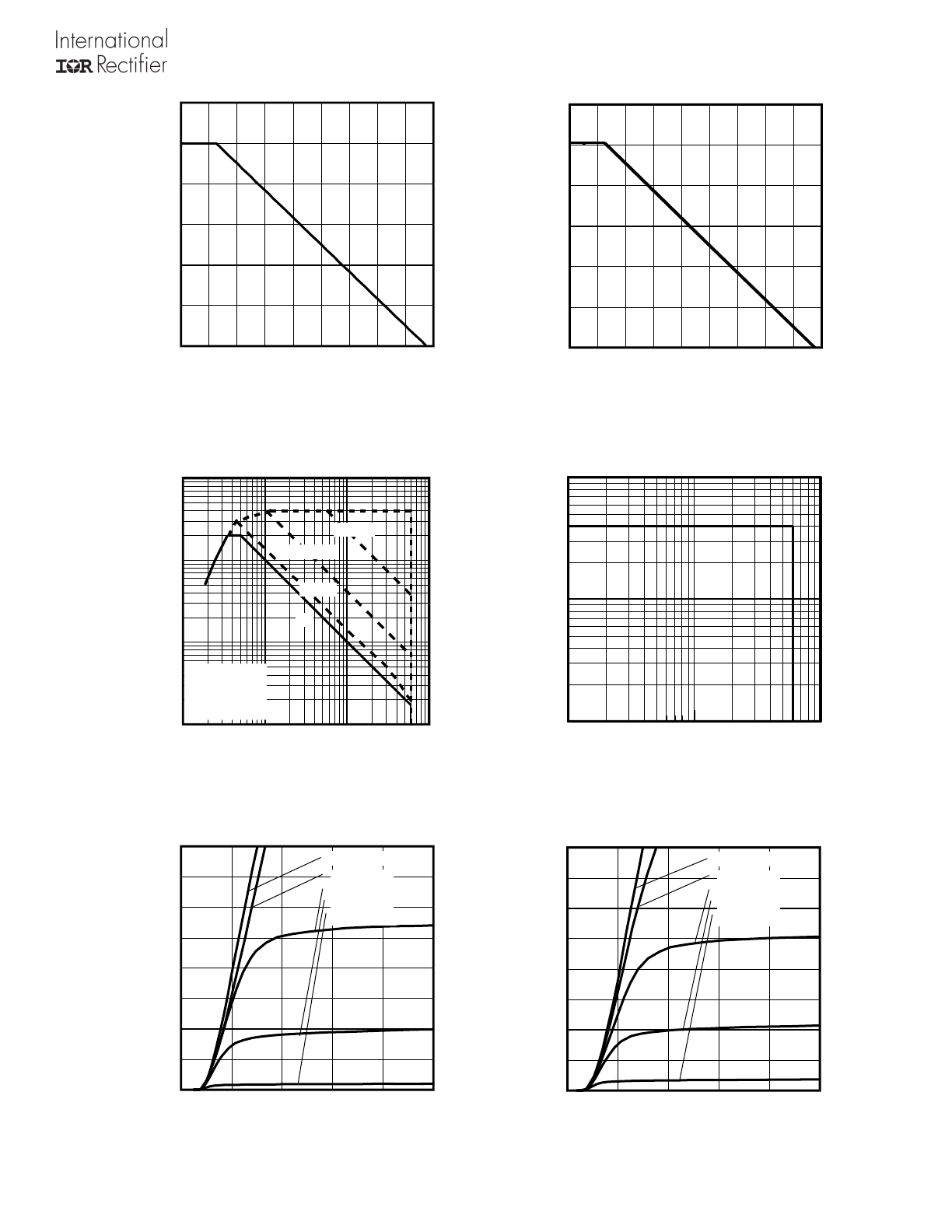
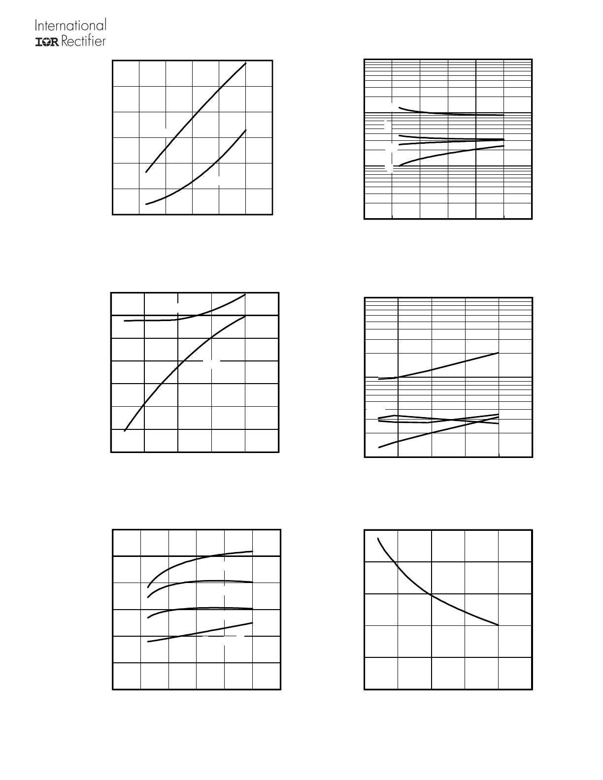
Fig. 1 - Maximum DC Collector Current vs.
Case Temperature
Fig. 2 - Power Dissipation vs. Case
Temperature
Fig. 4 - Reverse Bias SOA
T
J
= 175°C; V
CE
= 15V
Fig. 5 - Typ. IGBT Output Characteristics
T
J
= -40°C; tp = 80μs
Fig. 6 - Typ. IGBT Output Characteristics
T
J
= 25°C; tp = 80μs
Fig. 3 - Forward SOA,
T
C
= 25°C; T
J
≤
175°C
0
20 40 60 80 100 120 140 160 180
TC (°C)
0
4
8
12
16
20
24
I C
(
A
)
0
20 40
60 80 100 120 140 160 180
TC (°C)
0
20
40
60
80
100
120
P
to
t (
W
)
10
100
1000
VCE (V)
1
10
100
I C
A
)
0
2
4
6
8
10
VCE (V)
0
10
20
30
40
I C
E
(
A
)
VGE = 18V
VGE = 15V
VGE = 12V
VGE = 10V
VGE = 8.0V
0
2
4
6
8
10
VCE (V)
0
10
20
30
40
I C
E
(
A
)
VGE = 18V
VGE = 15V
VGE = 12V
VGE = 10V
VGE = 8.0V
1
10
100
1000
VCE (V)
0.1
1
10
100
I C
(
A
)
10μsec
100μsec
Tc = 25°C
Tj = 175°C
Single Pulse
DC
1msec
IRGS4064DPbF
4
www.irf.com
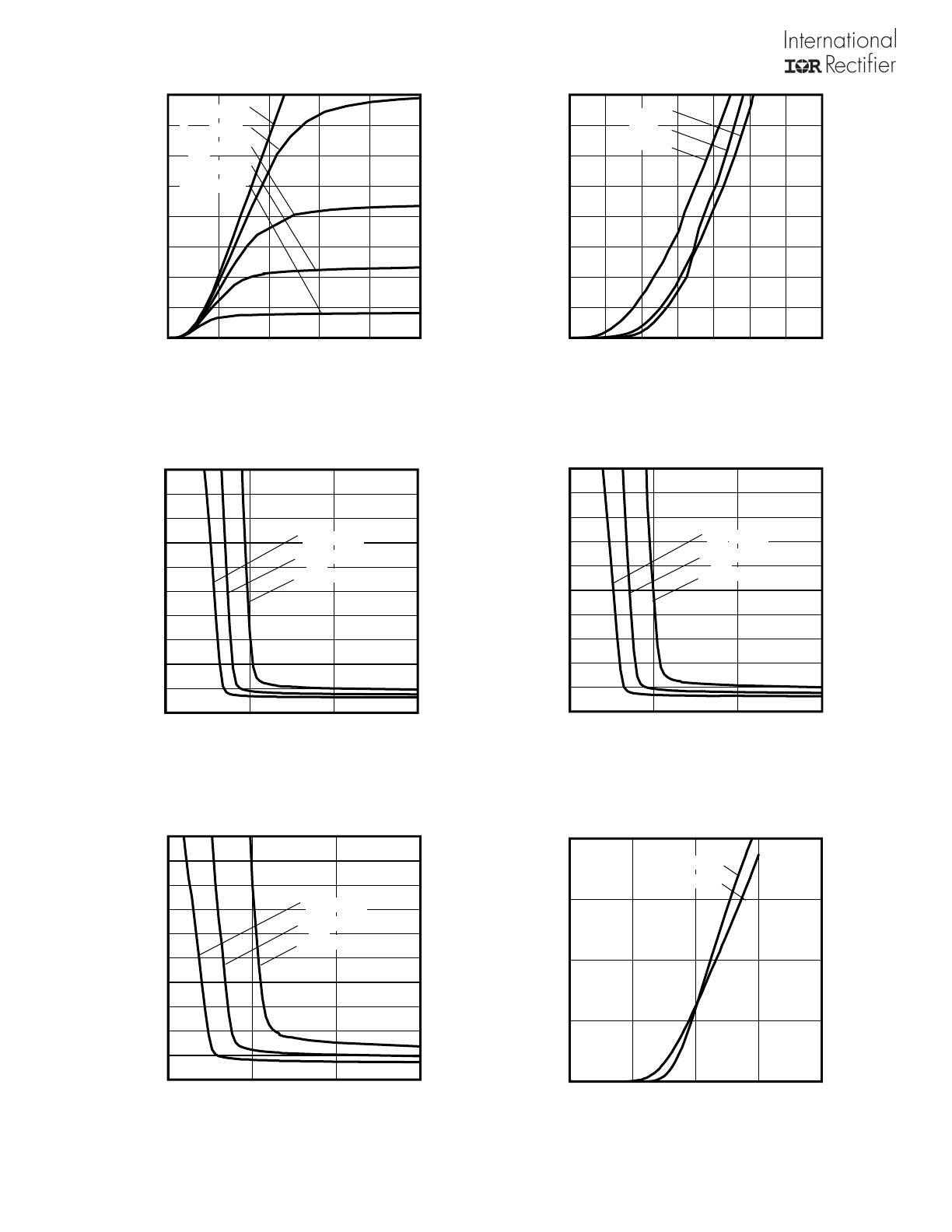
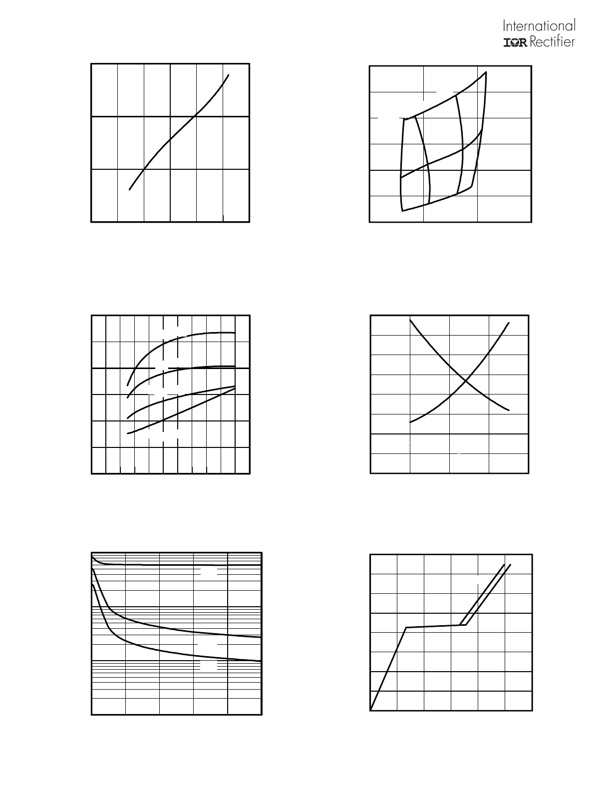
Fig. 9 - Typical V
CE
vs. V
GE
T
J
= -40°C
Fig. 7 - Typ. IGBT Output Characteristics
T
J
= 175°C; tp = 80μs
Fig. 10 - Typical V
CE
vs. V
GE
T
J
= 25°C
Fig. 8 - Typ. Diode Forward Characteristics
tp = 80μs
Fig. 12 - Typ. Transfer Characteristics
V
CE
= 50V; tp = 10μs
Fig. 11 - Typical V
CE
vs. V
GE
T
J
= 175°C
0
5
10
15
20
VGE (V)
0
10
20
30
40
I C
E
(
A
)
TJ = 25°C
TJ = 175°C
0
2
4
6
8
10
VCE (V)
0
10
20
30
40
I C
E
(
A
)
VGE = 18V
VGE = 15V
VGE = 12V
VGE = 10V
VGE = 8.0V
0.0
1.0
2.0
3.0
4.0
5.0
6.0
7.0
VF (V)
0
10
20
30
40
50
60
70
80
I F
(
A
)
-40°C
25°C
175°C
5
10
15
20
VGE (V)
0
2
4
6
8
10
12
14
16
18
20
V
C
E
(
V
)
ICE = 5.0A
ICE = 10A
ICE = 20A
5
10
15
20
VGE (V)
0
2
4
6
8
10
12
14
16
18
20
V
C
E
(
V
)
ICE = 5.0A
ICE = 10A
ICE = 20A
5
10
15
20
VGE (V)
0
2
4
6
8
10
12
14
16
18
20
V
C
E
(
V
)
ICE = 5.0A
ICE = 10A
ICE = 20A
IRGS4064DPbF
www.irf.com
5
Fig. 13 - Typ. Energy Loss vs. I
C
T
J
= 175°C; L = 1mH; V
CE
= 400V, R
G
= 22
Ω; V
GE
= 15V.
Fig. 15 - Typ. Energy Loss vs. R
G
T
J
= 175°C; L = 1mH; V
CE
= 400V, I
CE
= 10A; V
GE
= 15V
Fig. 14 - Typ. Switching Time vs. I
C
T
J
= 175°C; L=1mH; V
CE
= 400V
R
G
= 22
Ω; V
GE
= 15V
Fig. 16- Typ. Switching Time vs. R
G
T
J
= 175°C; L=1mH; V
CE
= 400V
I
CE
= 10A; V
GE
= 15V
Fig. 17 - Typical Diode I
RR
vs. I
F
T
J
= 175°C
Fig. 18 - Typical Diode I
RR
vs. R
G
T
J
= 175°C; I
F
= 10A
0
4
8
12
16
20
24
IC (A)
0
100
200
300
400
500
600
E
ne
rg
y
(μ
J)
EOFF
EON
0
4
8
12
16
20
24
IC (A)
1
10
100
1000
S
w
ic
hi
ng
T
im
e
(n
s)
tR
tdOFF
tF
tdON
0
25
50
75
100
125
RG (Ω)
0
50
100
150
200
250
300
350
E
ne
rg
y
(μ
J)
EON
EOFF
0
25
50
75
100
125
RG (Ω)
10
100
1000
S
w
ic
hi
ng
T
im
e
(n
s)
tR
tdOFF
tF
tdON
0
4
8
12
16
20
24
IF (A)
0
4
8
12
16
20
24
I R
R
(
A
)
RG = 100 Ω
RG =10 Ω
RG =22 Ω
RG =47 Ω
0
25
50
75
100
125
RG (Ω)
0
4
8
12
16
20
I R
R
(
A
)
IRGS4064DPbF
6
www.irf.com
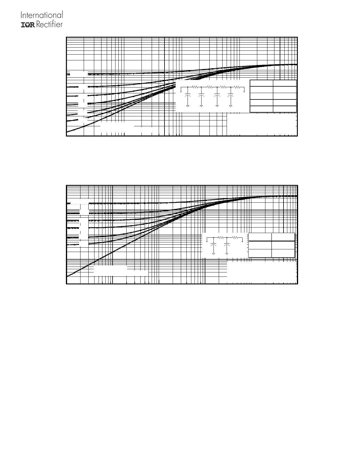
Fig. 20 - Typical Diode Q
RR
V
CC
= 400V; V
GE
= 15V; T
J
= 175°C
Fig. 19- Typical Diode I
RR
vs. di
F
/dt
V
CC
= 400V; V
GE
= 15V;
I
CE
= 10A; T
J
= 175°C
Fig. 24 - Typical Gate Charge
vs. V
GE
I
CE
= 10A, L=600μH
Fig. 23- Typ. Capacitance vs. V
CE
V
GE
= 0V; f = 1MHz
Fig. 22- Typ. V
GE
vs Short Circuit Time
V
CC
=400V, T
C
=25°C
Fig. 21 - Typical Diode E
RR
vs. I
F
T
J
= 175°C
0
200
400
600
800
1000 1200
diF /dt (A/μs)
5
10
15
20
I R
R
(
A
)
0
2
4
6
8 10 12 14 16 18 20 22
IF (A)
0
50
100
150
200
250
300
I R
R
(
A
)
RG = 10Ω
RG = 22Ω
RG = 47Ω
RG = 100Ω
8
10
12
14
16
VGE (V)
0
2
4
6
8
10
12
14
16
T
im
e
(μ
s)
0
10
20
30
40
50
60
70
80
C
ur
re
nt
(A
)
Tsc
Isc
0
500
1000
1500
diF /dt (A/μs)
300
400
500
600
700
800
900
Q
R
R
(
nC
)
10
Ω
22
Ω
47
Ω
100
Ω
20A
10A
5.0A
0
4
8
12
16
20
24
Q G, Total Gate Charge (nC)
0
2
4
6
8
10
12
14
16
V
G
E
(
V
)
300V
400V
0
20
40
60
80
100
VCE (V)
1
10
100
1000
C
ap
ac
ita
nc
e
(p
F
)
Cies
Coes
Cres
IRGS4064DPbF
www.irf.com
7
Fig. 26. Maximum Transient Thermal Impedance, Junction-to-Case (DIODE)
Fig 25. Maximum Transient Thermal Impedance, Junction-to-Case (IGBT)
1E-006
1E-005
0.0001
0.001
0.01
t1 , Rectangular Pulse Duration (sec)
0.01
0.1
1
10
T
he
rm
al
R
es
po
ns
e
(
Z
th
JC
)
0.20
0.10
D = 0.50
0.02
0.01
0.05
SINGLE PULSE
( THERMAL RESPONSE )
Notes:
1. Duty Factor D = t1/t2
2. Peak Tj = P dm x Zthjc + Tc
1E-006
1E-005
0.0001
0.001
0.01
0.1
t1 , Rectangular Pulse Duration (sec)
0.001
0.01
0.1
1
10
T
he
rm
al
R
es
po
ns
e
(
Z
th
JC
)
0.20
0.10
D = 0.50
0.02
0.01
0.05
SINGLE PULSE
( THERMAL RESPONSE )
Notes:
1. Duty Factor D = t1/t2
2. Peak Tj = P dm x Zthjc + Tc
Ri (°C/W)
τι (sec)
1.939783 0.000975
1.721867 0.006135
τ
J
τ
J
τ
1
τ
1
τ
2
τ
2
R
1
R
1
R
2
R
2
τ
C
C
Ci=
τi/Ri
Ri (°C/W)
τι (sec)
0.007362
0
0.342317 0.000048
0.647826 0.000192
0.493231 0.001461
τ
J
τ
J
τ
1
τ
1
τ
2
τ
2
τ
3
τ
3
R
1
R
1
R
2
R
2
R
3
R
3
Ci i
/Ri
Ci=
τi/Ri
τ
τ
C
τ
4
τ
4
R
4
R
4
IRGS4064DPbF
8
www.irf.com
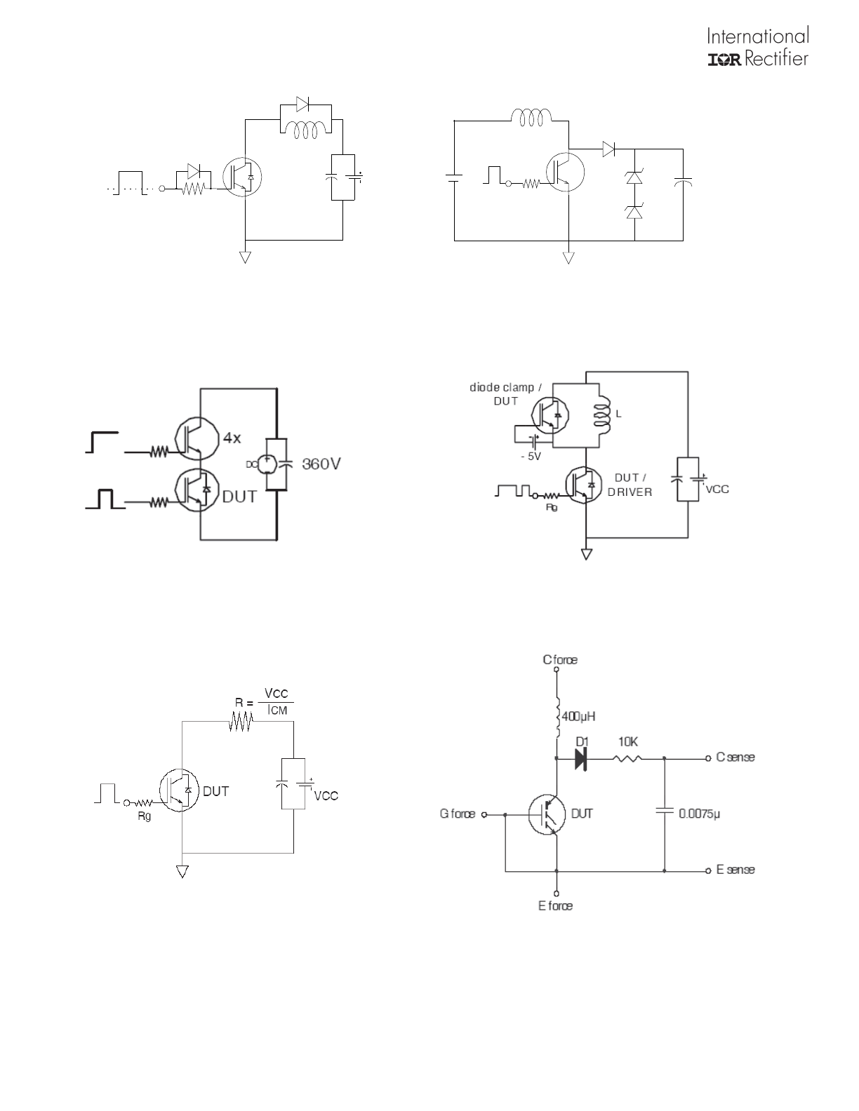
Fig.C.T.1 - Gate Charge Circuit (turn-off)
Fig.C.T.2 - RBSOA Circuit
1K
VCC
DUT
0
L
Fig.C.T.3 - S.C.SOA Circuit
Fig.C.T.4 - Switching Loss Circuit
L
Rg
80 V
DUT
480V
+
-
Fig.C.T.5 - Resistive Load Circuit
Fig.C.T.6 - Typical Filter Circuit for
V
(BR)CES
Measurement
IRGS4064DPbF
www.irf.com
9
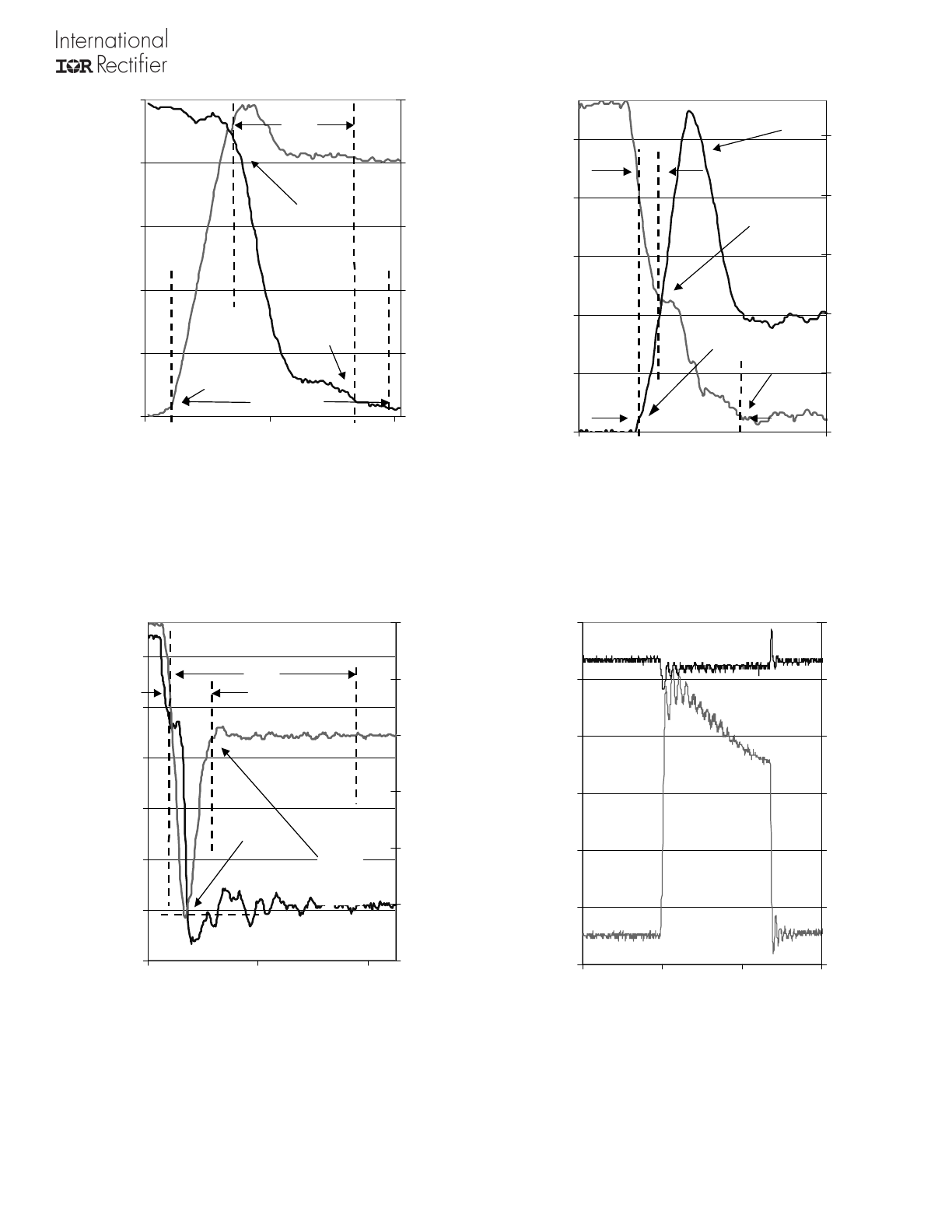
Fig. WF1 - Typ. Turn-off Loss Waveform
@ T
J
= 175°C using Fig. CT.4
Fig. WF2 - Typ. Turn-on Loss Waveform
@ T
J
= 175°C using Fig. CT.4
WF.3- Typ. Reverse Recovery Waveform
@ T
J
= 175°C using CT.4
WF.4- Typ. Short Circuit Waveform
@ T
J
= 25°C using CT.3
0
100
200
300
400
500
-0.04
0.06
0.16
time(μs)
V
CE
(V
)
0
2
4
6
8
10
I
CE
(A
)
90% I
CE
5% V
CE
5% I
CE
Eoff Loss
tf
-25
50
125
200
275
350
-0.1
0.1
time (μs)
V
CE
(V
)
0
5
10
15
20
25
I
CE
(A
)
TEST CURRENT
90% test current
5% V
CE
10% test current
tr
Eon Loss
-475
-400
-325
-250
-175
-100
-25
-0.05
0.15
0.35
time (μS)
V
F
(V
)
-20
-15
-10
-5
0
5
10
I
F
(A
)
Peak
I
RR
t
RR
Q
RR
10%
Peak
IRR
-10
10
30
50
70
90
110
-5
0
5
10
Time (uS)
Vc
e (
V
)
0
75
150
225
300
375
450
Ic
e
(A
)
VC
IC
IRGS4064DPbF
10
www.irf.com
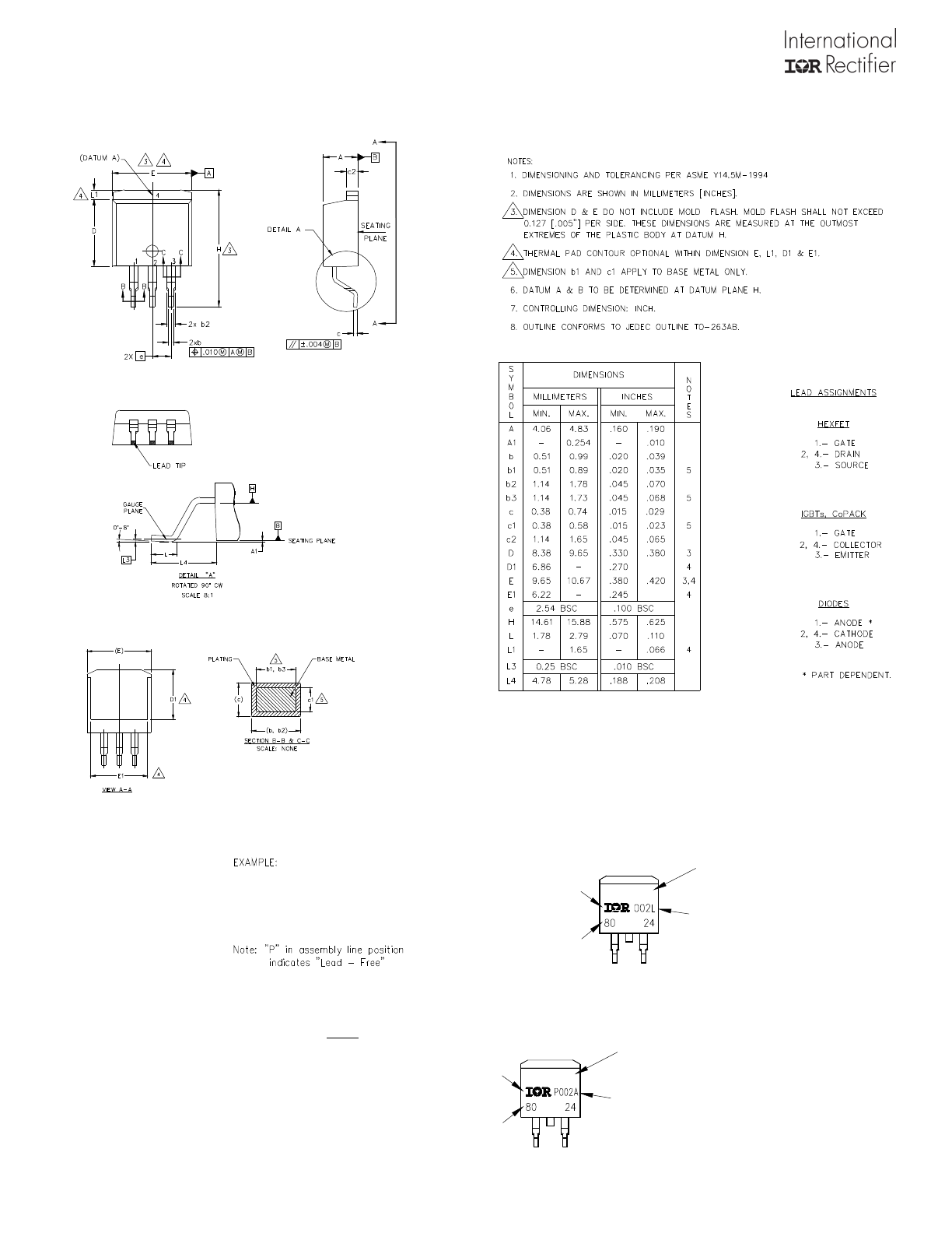
D
2
Pak Part Marking Information
D
2
Pak Package Outline
(Dimensions are shown in millimeters (inches))
DATE CODE
YEAR 0 = 2000
WEEK 02
A = ASSEMBLY SITE CODE
RECTIFIER
INTERNATIONAL
PART NUMBER
P = DESIGNATES LEAD - FREE
PRODUCT (OPTIONAL)
F530S
IN THE ASSEMBLY LINE "L"
ASSEMBLED ON WW 02, 2000
THIS IS AN IRF530S WITH
LOT CODE 8024
INTERNATIONAL
LOGO
RECTIFIER
LOT CODE
ASSEMBLY
YEAR 0 = 2000
PART NUMBER
DATE CODE
LINE L
WEEK 02
OR
F530S
LOGO
ASSEMBLY
LOT CODE