
Insulated Gate Bipolar Transistor with Ultrafast Soft Recovery Diode
V
CES
= 600V
I
C
= 10A, T
C
= 100°C
t
sc
> 5µs, T
jmax
= 175°C
V
CE(on) typ.
= 1.7V @ 6A
G
C
E
Gate
Collector
Em itter
E
G
n-channel
C
D
2
-Pak
IRGS4610DPbF
G
C
E
Applications
•
Appliance Drives
•
Inverters
•
UPS
Features
Benefits
Low V
CE(ON)
and switching losses
High efficiency in a wide range of applications and switching frequencies
Square RBSOA and maximum junction temperature 175°C
Improved reliability due to rugged hard switching performance and higher
power capability
Positive V
CE(ON)
temperature coefficient and tighter distribution of
parameters
Excellent current sharing in parallel operation
5μs short circuit SOA
Enables short circuit protection scheme
Lead-free, RoHS compliant
Environmentally friendly
→
D-Pak
IRGR4610DPbF
TO-220AB
IRGB4610DPbF
C
E
C
G
G
C
E
IRGR4610DPbF
IRGS4610DPbF
IRGB4610DPbF
1
www.irf.com
©
2014 International Rectifier
Submit Datasheet Feedback
November 14, 2014
Base part number
Package Type
Orderable Part Number
Form
Quantity
Tube
75
IRGR4610DPbF
Tape and Reel
2000
IRGR4610DTRPbF
Tape and Reel Right
3000
IRGR4610DTRRPbF
Tape and Reel Left
3000
IRGR4610DTRLPbF
Tube
50
IRGS4610DPbF
Tape and Reel Right
800
IRGS4610DTRRPbF
Tape and Reel Left
800
IRGS4610DTRLPbF
IRGB4610DPbF
TO-220AB
Tube
50
IRGB4610DPbF
Standard Pack
D
2
PAK
D-PAK
IRGR4610DPbF
IRGS4610DPbF
Absolute Maximum Ratings
Parameter
Max.
Units
V
CES
Collector-to-Emitter Breakdown Voltage
V
I
C
@ T
C
= 25°C
Continuous Collector Current
I
C
@ T
C
= 100°C
Continuous Collector Current
I
CM
Pulsed Collector Current, V
GE
= 15V
I
LM
Clamped Inductive Load Current, V
GE
= 20V c
A
I
F
@ T
C
= 25°C
Diode Continuous Forward Current
I
F
@ T
C
=100°C
Diode Continuous Forward Current
I
FM
Diode Maximum Forward Current f
Continuous Gate-to-Emitter Voltage
V
Transient Gate-to-Emitter Voltage
P
D
@ T
C
=25°
Maximum Power Dissipation
W
P
D
@ T
C
=100°
Maximum Power Dissipation
T
J
Operating Junction and
T
STG
Storage Temperature Range
Soldering Temperature, for 10 seconds (1.6mm from case)
Mounting Torque, 6-32 or M3 Screw TO-220
24
-40 to + 175
10lbf. In (1.1 N.m)
± 20
± 30
77
39
°C
300
V
GE
600
16
10
18
24
10
6
IRGR/S/B4610DPbF
2
www.irf.com
©
2014 International Rectifier
Submit Datasheet Feedback
November 14, 2014
Notes:
V
CC
= 80% (V
CES
), V
GE
= 20V, L = 1.0mH, R
G
= 100
Ω.
R
θ
is measured at T
J
approximately 90°C
.
Refer to AN-1086 for guidelines for measuring V
(BR)CES
safely.
Pulse width limited by max. junction temperature.
Values influenced by parasitic L and C in measurement
When mounted on 1" square PCB (FR-4 or G-10 Material). For recommended footprint and soldering techniques refer to application
note #AN-994
: http://www.irf.com/technical-info/appnotes/an-994.pdf
Thermal Resistance
Parameter
Min.
Typ.
Max. Units
R
θJC
Thermal Resistance, Junction-to-Case -(IGBT)d
–––
–––
1.9
R
θJC
Thermal Resistance, Junction-to-Case -(Diode)d
–––
–––
6.3
R
θCS
Thermal Resistance, Case-to-Sink (flat, greased surface) (TO-220)
–––
0.5
–––
Thermal Resistance, Junction-to-Ambient (PCB mount) (D-PAK)h
–––
–––
50
Thermal Resistance, Junction-to-Ambient (D-PAK)
–––
–––
110
Thermal Resistance, Junction-to-Ambient (PCB mount, Steady State)
(D
2
PAK)h
–––
–––
40
Thermal Resistance, Junction-to-Ambient ( Socket mount) (TO-220)
–––
–––
62
R
θJA
°C/W
Electrical Characteristics @ T
J
= 25°C (unless otherwise specified)
Parameter
Min.
Typ.
Max. Units Conditions
V
(BR)CES
Collector-to-Emitter Breakdown Voltage
600
—
—
V
V
GE
= 0V, I
c
=100 μA e
ΔV
(BR)CES
/ΔT
J
Temperature Coeff. of Breakdown Voltage
—
0.36
—
V/°C V
GE
= 0V, I
c
= 250μA ( 25 -175
o
C )
—
1.7
2.0
I
C
= 6.0A, V
GE
= 15V, T
J
= 25°C
V
CE(on)
Collector-to-Emitter Saturation Voltage
—
2.07
—
V
I
C
= 6.0A, V
GE
= 15V, T
J
= 150°C
—
2.14
—
I
C
= 6.0A, V
GE
= 15V, T
J
= 175°C
V
GE(th)
Gate Threshold Voltage
4.0
—
6.5
V
V
CE
= V
GE
, I
C
= 150μA
ΔV
GE(th)
/ΔTJ Threshold Voltage temp. coefficient
—
-13
—
mV/°C V
CE
= V
GE
, I
C
= 250μA ( 25 -175
o
C )
gfe
Forward Transconductance
—
5.8
—
S
V
CE
= 25V, I
C
= 6.0A, PW =80μS
I
CES
—
—
25
μA
V
GE
= 0V,V
CE
= 600V
—
—
250
V
GE
= 0V, V
CE
= 600V, T
J
=175°C
V
FM
—
1.60
2.30
V
I
F
= 6.0A
—
1.30
—
I
F
= 6.0A, T
J
= 175°C
I
GES
Gate-to-Emitter Leakage Current
—
—
±100
nA
V
GE
= ± 20 V
Diode Forward Voltage Drop
Collector-to-Emitter Leakage Current
IRGR/S/B4610DPbF
3
www.irf.com
©
2014 International Rectifier
Submit Datasheet Feedback
November 14, 2014
Switching Characteristics @ T
J
= 25°C (unless otherwise specified)
Parameter
Min.
Typ.
Max. Units
Q
g
Total Gate Charge (turn-on)
—
13
—
I
C
= 6.0A
Q
ge
Gate-to-Emitter Charge (turn-on)
—
3.0
—
nC
V
CC
= 400V
Q
gc
Gate-to-Collector Charge (turn-on)
—
6.4
—
V
GE
= 15V
E
on
Turn-On Switching Loss
—
56
—
I
C
= 6.0A, V
CC
= 400V, V
GE
= 15V
E
off
Turn-Off Switching Loss
—
122
—
μJ
R
G
= 47Ω, L=1mH, L
S
= 150nH, T
J
= 25°C
E
total
Total Switching Loss
—
178
—
Energy losses include tail and diode reverse recovery
t
d(on)
Turn-On delay time
—
27
—
I
C
= 6.0A, V
CC
= 400V
t
r
Rise time
—
11
—
ns
R
G
= 47Ω, L=1mH, L
S
= 150nH
t
d(off)
Turn-Off delay time
—
75
—
T
J
= 25°C g
t
f
Fall time
—
17
—
E
on
Turn-On Switching Loss
—
140
—
I
C
= 6.0A, V
CC
= 400V, V
GE
= 15V
E
off
Turn-Off Switching Loss
—
189
—
μJ R
G
= 47Ω, L=1mH, L
S
= 150nH, T
J
= 175°C
E
total
Total Switching Loss
—
329
—
Energy losses include tail and diode reverse recovery
t
d(on)
Turn-On delay time
—
26
—
I
C
= 6.0A, V
CC
= 400V
t
r
Rise time
—
12
—
ns
R
G
= 47Ω, L=1mH, L
S
= 150nH
t
d(off)
Turn-Off delay time
—
95
—
T
J
= 175°C g
t
f
Fall time
—
32
—
C
ies
Input Capacitance
—
350
—
V
GE
= 0V
C
oes
Output Capacitance
—
29
—
V
CC
= 30V
C
res
Reverse Transfer Capacitance
—
10
—
f = 1Mhz
T
J
= 175°C, I
C
= 24A
RBSOA
Reverse Bias Safe Operating Area
FULL SQUARE
V
CC
= 500V, Vp =600V
R
G
= 100Ω, V
GE
= +20V to 0V
V
CC
= 400V, Vp =600V
R
G
= 100Ω, V
GE
= +15V to 0V
Erec
Reverse recovery energy of the diode
—
178
—
μJ
T
J
= 175
o
C
trr
Diode Reverse recovery time
—
74
—
ns
V
CC
= 400V, I
F
= 6.0A
Irr
Peak Reverse Recovery Current
—
12
—
A
V
GE
= 15V, Rg = 47Ω, L=1mH, L
S
=150nH
μs
pF
Conditions
—
SCSOA
Short Circuit Safe Operating Area
—
5
IRGR/S/B4610DPbF
4
www.irf.com
©
2014 International Rectifier
Submit Datasheet Feedback
November 14, 2014
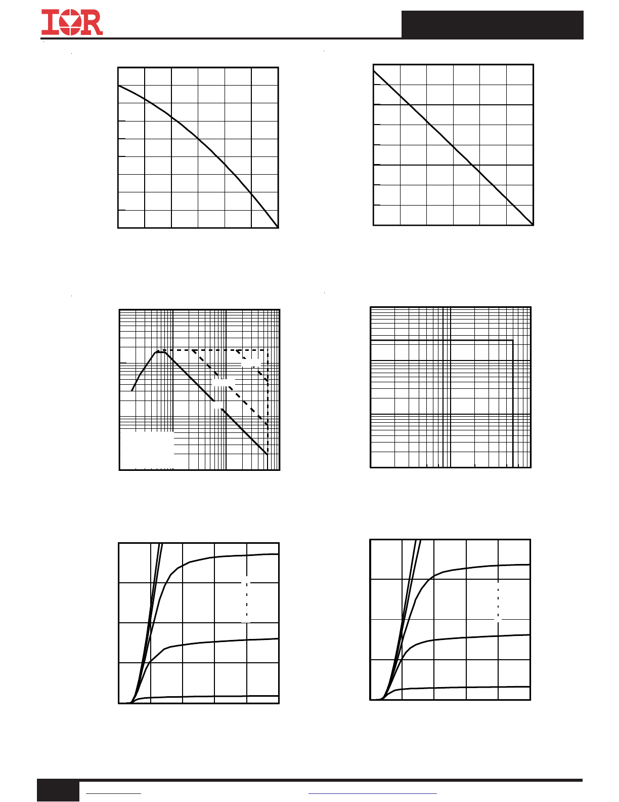
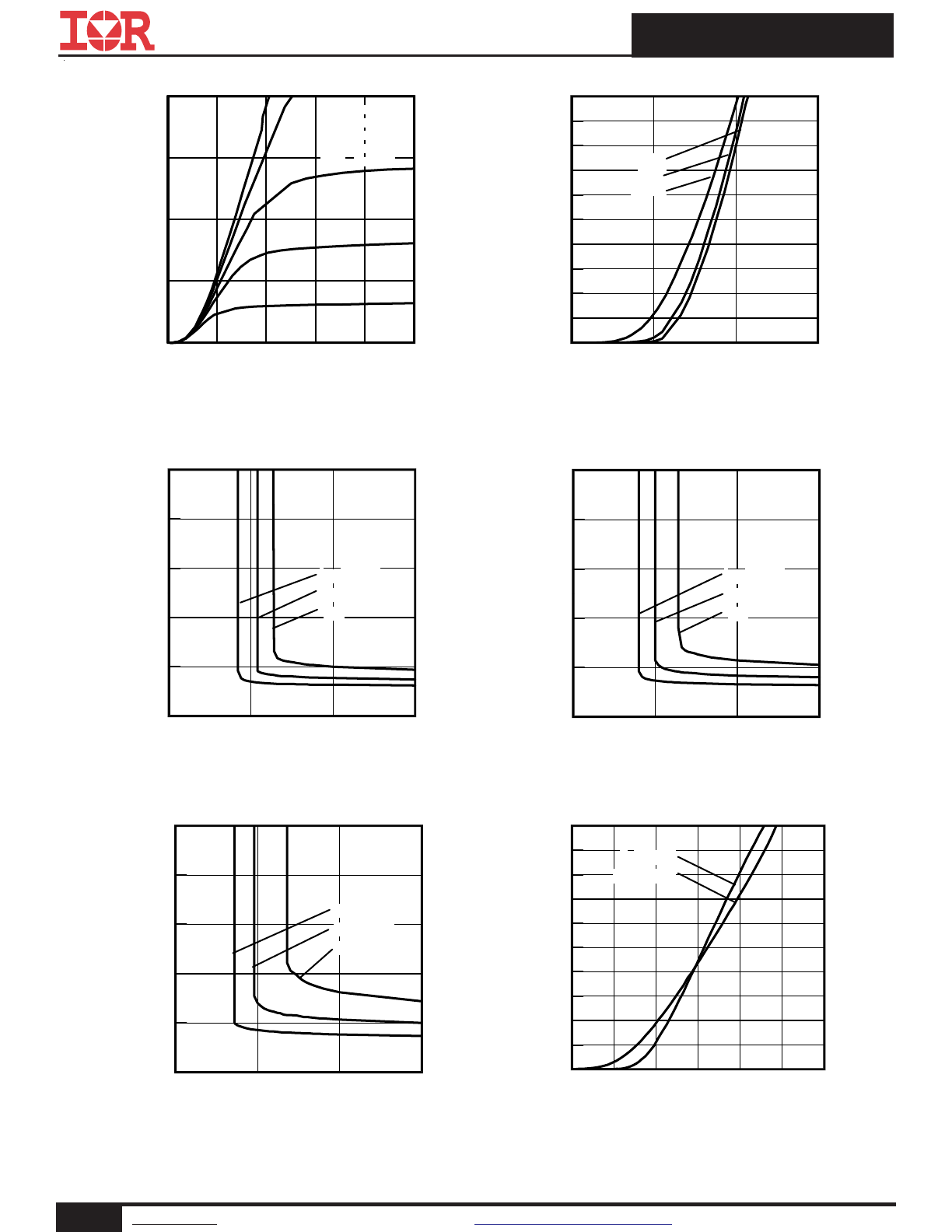
Fig. 1 - Maximum DC Collector Current vs.
Case Temperature
Fig. 2 - Power Dissipation vs. Case
Temperature
Fig. 4 - Reverse Bias SOA
T
J
= 175°C, V
GE
= 20V
Fig. 5 - Typ. IGBT Output Characteristics
T
J
= -40°C; tp = 80μs
Fig. 6 - Typ. IGBT Output Characteristics
T
J
= 25°C; tp = 80μs
Fig. 3 - Forward SOA,
T
C
= 25°C, T
J
≤
175°C, V
GE
= 15V
0
2
4
6
8
10
VCE (V)
0
5
10
15
20
I C
E
(
A
)
Top
V
GE
= 18V
V
GE
= 15V
V
GE
= 12V
V
GE
= 10V
Bottom V
GE
= 8.0V
0
2
4
6
8
10
VCE (V)
0
5
10
15
20
I C
E
(
A
)
Top
VGE = 18V
VGE = 15V
VGE = 12V
VGE = 10V
Bottom VGE = 8.0V
25
50
75
100
125
150
175
TC (°C)
0
2
4
6
8
10
12
14
16
18
I C
(
A
)
25
50
75
100
125
150
175
TC (°C)
0
10
20
30
40
50
60
70
80
P
to
t
(W
)
10
100
1000
VCE (V)
0
1
10
100
I C
A
)
1
10
100
1000
VCE (V)
0.1
1
10
100
I C
(
A
)
10μsec
100μsec
Tc = 25°C
Tj = 175°C
Single Pulse
DC
IRGR/S/B4610DPbF
5
www.irf.com
©
2014 International Rectifier
Submit Datasheet Feedback
November 14, 2014
Fig. 9 - Typical V
CE
vs. V
GE
T
J
= -40°C
Fig. 7 - Typ. IGBT Output Characteristics
T
J
= 175°C; tp = 80μs
Fig. 10 - Typical V
CE
vs. V
GE
T
J
= 25°C
Fig. 8 - Typ. Diode Forward Characteristics
tp = 80μs
Fig. 12 - Typ. Transfer Characteristics
V
CE
= 50V; tp = 10μs
Fig. 11 - Typical V
CE
vs. V
GE
T
J
= 175°C
0.0
1.0
2.0
3.0
VF (V)
0
2
4
6
8
10
12
14
16
18
20
I F
(
A
)
-40°C
25°C
175°C
5
10
15
20
VGE (V)
0
2
4
6
8
10
V
C
E
(
V
)
ICE = 3.0A
ICE = 6.0A
ICE = 12A
5
10
15
20
VGE (V)
0
2
4
6
8
10
V
C
E
(
V
)
ICE = 3.0A
ICE = 6.0A
ICE = 12A
5
10
15
20
VGE (V)
0
2
4
6
8
10
V
C
E
(
V
)
ICE = 3.0A
ICE = 6.0A
ICE = 12A
0
2
4
6
8
10
VCE (V)
0
5
10
15
20
I C
E
(
A
)
Top
V
GE
= 18V
V
GE
= 15V
V
GE
= 12V
V
GE
= 10V
Bottom V
GE
= 8.0V
4
6
8
10
12
14
16
VGE, Gate-to-Emitter Voltage (V)
0
2
4
6
8
10
12
14
16
18
20
I C
, C
ol
le
ct
or
-t
o-
E
m
itt
er
C
ur
re
nt
(
A
)
TJ = 25°C
TJ = 175°C
IRGR/S/B4610DPbF
6
www.irf.com
©
2014 International Rectifier
Submit Datasheet Feedback
November 14, 2014
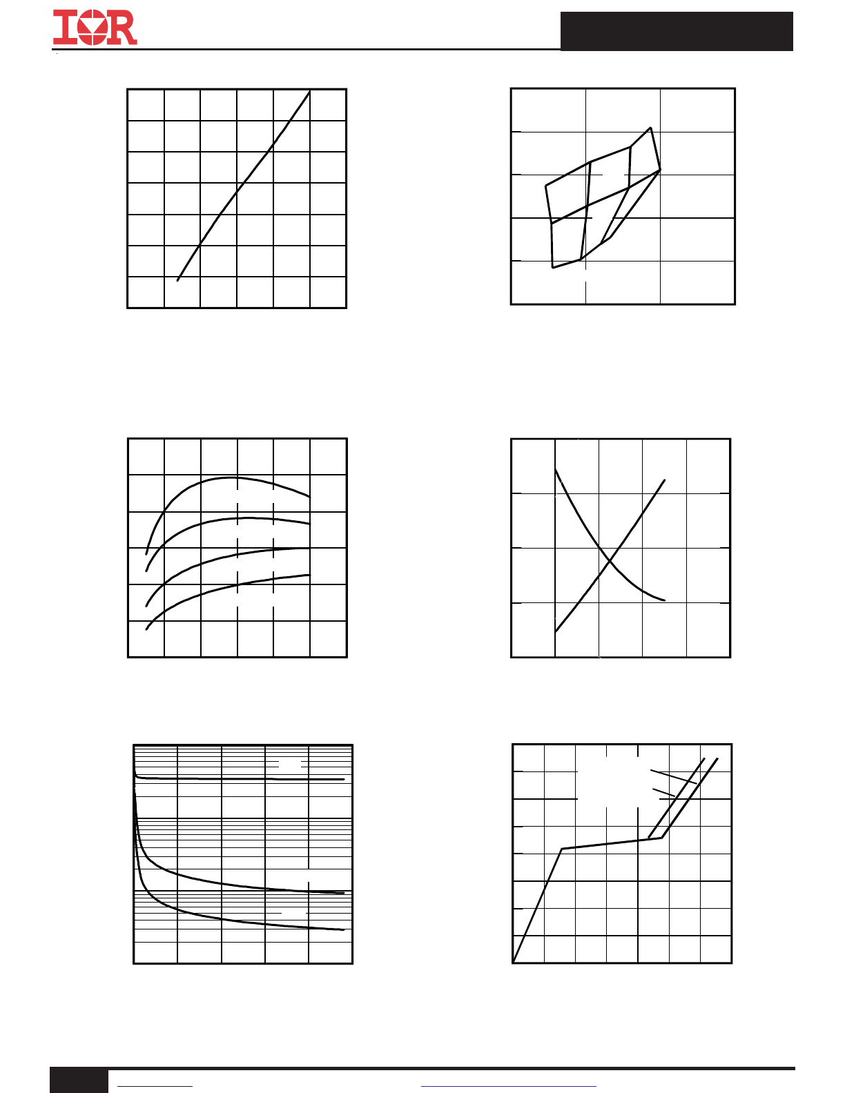
Fig. 13 - Typ. Energy Loss vs. I
C
T
J
= 175°C; L = 1mH; V
CE
= 400V, R
G
= 47
Ω; V
GE
= 15V.
Fig. 15 - Typ. Energy Loss vs. R
G
T
J
= 175°C; L = 1mH; V
CE
= 400V, I
CE
= 6.0A; V
GE
= 15V
Fig. 14 - Typ. Switching Time vs. I
C
T
J
= 175°C; L=1mH; V
CE
= 400V
R
G
= 47
Ω; V
GE
= 15V
Fig. 16- Typ. Switching Time vs. R
G
T
J
= 175°C; L=1mH; V
CE
= 400V
I
CE
= 6.0A; V
GE
= 15V
Fig. 17 - Typical Diode I
RR
vs. I
F
T
J
= 175°C
Fig. 18 - Typical Diode I
RR
vs. R
G
T
J
= 175°C; I
F
= 6.0A
0
2
4
6
8
10
12
14
IC (A)
50
100
150
200
250
300
350
400
E
ne
rg
y
(μ
J)
EOFF
EON
2
4
6
8
10
12
14
IC (A)
1
10
100
1000
S
w
ic
hi
ng
T
im
e
(n
s)
tR
tdOFF
tF
tdON
0
25
50
75
100
125
Rg (
Ω)
60
80
100
120
140
160
180
200
220
E
ne
rg
y
(μ
J)
EOFF
EON
0
25
50
75
100
125
RG (Ω)
1
10
100
1000
S
w
ic
hi
ng
T
im
e
(n
s)
tR
tdOFF
tF
tdON
2
4
6
8
10
12
14
IF (A)
0
5
10
15
20
25
30
I R
R
(
A
)
RG = 10Ω
RG = 22Ω
RG = 47Ω
RG = 100Ω
0
25
50
75
100
125
RG (Ω)
6
8
10
12
14
16
18
20
22
I R
R
(
A
)
IRGR/S/B4610DPbF
7
www.irf.com
©
2014 International Rectifier
Submit Datasheet Feedback
November 14, 2014
Fig. 20 - Typical Diode Q
RR
V
CC
= 400V; V
GE
= 15V; T
J
= 175°C
Fig. 19- Typical Diode I
RR
vs. di
F
/dt
V
CC
= 400V; V
GE
= 15V;
I
CE
= 6.0A; T
J
= 175°C
Fig. 24 - Typical Gate Charge
vs. V
GE
I
CE
= 6.0A, L=600μH
Fig. 23- Typ. Capacitance vs. V
CE
V
GE
= 0V; f = 1MHz
Fig. 22- Typ. V
GE
vs. Short Circuit Time
V
CC
=400V, T
C
=25°C
Fig. 21 - Typical Diode E
RR
vs. I
F
T
J
= 175°C
0
100
200
300
400
500
VCE (V)
1
10
100
1000
C
ap
ac
ita
nc
e
(p
F
)
Cies
Coes
Cres
0
200
400
600
800
1000 1200
diF /dt (A/μs)
6
8
10
12
14
16
18
20
I R
R
(
A
)
2
4
6
8
10
12
14
IF (A)
50
100
150
200
250
300
350
E
ne
rg
y
(μ
J)
RG = 10Ω
RG = 22Ω
RG = 47Ω
RG = 100Ω
8
10
12
14
16
18
VGE (V)
0
5
10
15
20
T
im
e
(
μs
)
10
20
30
40
50
C
ur
re
nt
(A
)
Tsc
Isc
0
2
4
6
8
10
12
14
Q G, Total Gate Charge (nC)
0
2
4
6
8
10
12
14
16
V
G
E
, G
at
e-
to
-E
m
itt
er
V
ol
ta
ge
(
V
)
VCES = 400V
VCES = 300V
0
500
1000
1500
diF /dt (A/μs)
200
400
600
800
1000
1200
Q
R
R
(
nC
)
10Ω
22Ω
100Ω
47Ω
6.0A
12A
3.0A
IRGR/S/B4610DPbF
8
www.irf.com
©
2014 International Rectifier
Submit Datasheet Feedback
November 14, 2014
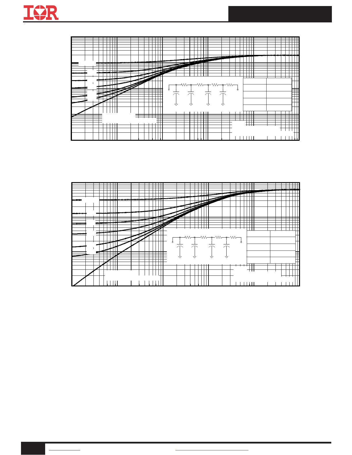
Fig. 26. Maximum Transient Thermal Impedance, Junction-to-Case (DIODE)
Fig 25. Maximum Transient Thermal Impedance, Junction-to-Case (IGBT)
1E-006
1E-005
0.0001
0.001
0.01
0.1
t1 , Rectangular Pulse Duration (sec)
0.001
0.01
0.1
1
10
T
he
rm
al
R
es
po
ns
e
(
Z
th
JC
)
0.20
0.10
D = 0.50
0.02
0.01
0.05
SINGLE PULSE
( THERMAL RESPONSE )
Notes:
1. Duty Factor D = t1/t2
2. Peak Tj = P dm x Zthjc + Tc
τ
J
τ
J
τ
1
τ
1
τ
2
τ
2
τ
3
τ
3
R
1
R
1
R
2
R
2
R
3
R
3
Ci i
/Ri
Ci=
τi/Ri
τ
τ
C
τ
4
τ
4
R
4
R
4
Ri (°C/W)
τi (sec)
0.0415 0.000005
0.7262 0.000076
0.7721 0.000810
0.4016 0.004929
1E-006
1E-005
0.0001
0.001
0.01
0.1
t1 , Rectangular Pulse Duration (sec)
0.01
0.1
1
10
T
he
rm
al
R
es
po
ns
e
(
Z
th
JC
)
0.20
0.10
D = 0.50
0.02
0.01
0.05
SINGLE PULSE
( THERMAL RESPONSE )
Notes:
1. Duty Factor D = t1/t2
2. Peak Tj = P dm x Zthjc + Tc
τ
J
τ
J
τ
1
τ
1
τ
2
τ
2
τ
3
τ
3
R
1
R
1
R
2
R
2
R
3
R
3
Ci i
/Ri
Ci=
τi/Ri
τ
τ
C
τ
4
τ
4
R
4
R
4
Ri (°C/W)
τi (sec)
0.2195 0.000023
1.7733 0.000165
2.9352 0.001493
1.3704 0.013255
IRGR/S/B4610DPbF
9
www.irf.com
©
2014 International Rectifier
Submit Datasheet Feedback
November 14, 2014
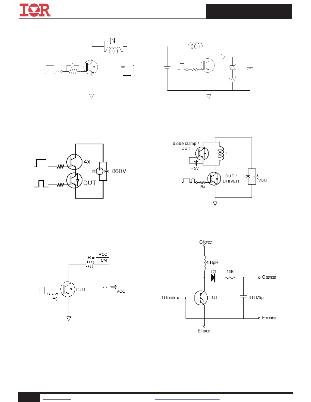
Fig.C.T.1 - Gate Charge Circuit (turn-off)
Fig.C.T.2 - RBSOA Circuit
1K
VCC
DUT
0
L
Fig.C.T.3 - S.C.SOA Circuit
Fig.C.T.4 - Switching Loss Circuit
L
Rg
80 V
DUT
480V
+
-
Fig.C.T.5 - Resistive Load Circuit
Fig.C.T.6 - Typical Filter Circuit for
V
(BR)CES
Measurement
IRGR/S/B4610DPbF
10
www.irf.com
©
2014 International Rectifier
Submit Datasheet Feedback
November 14, 2014
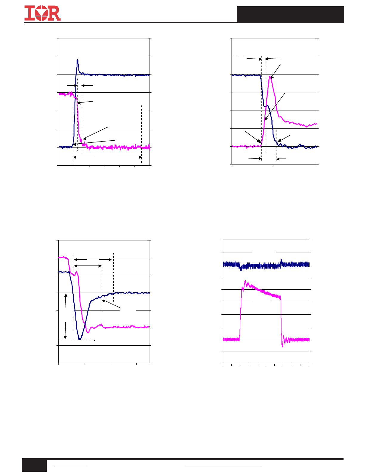
Fig. WF1 - Typ. Turn-off Loss Waveform
@ T
J
= 175°C using Fig. CT.4
Fig. WF2 - Typ. Turn-on Loss Waveform
@ T
J
= 175°C using Fig. CT.4
WF.3- Typ. Diode Recovery Waveform
@ T
J
= 175°C using CT.4
WF.4- Typ. Short Circuit Waveform
@ T
J
= 25°C using CT.3
0
50
100
150
200
250
300
350
400
450
500
-2 -1 0 1 2 3 4 5 6 7 8
Time (uS)
Vc
e (
V
)
-20
-10
0
10
20
30
40
50
60
70
80
V
CE
I
CE
-600
-500
-400
-300
-200
-100
0
100
-0.05
0.05
0.15
0.25
time (μS)
V
F
(V
)
-20
-15
-10
-5
0
5
10
15
Peak
I
RR
t
RR
Q
RR
10%
Peak
IRR
-100
0
100
200
300
400
500
600
-0.2
0
0.2
0.4
0.6
0.8
1
time(μs)
V
CE
(V
)
-2
0
2
4
6
8
10
12
90% I
CE
5% V
CE
5% I
CE
Eoff Loss
tf
-100
0
100
200
300
400
500
600
4.3
4.5
4.7
time (μs)
V
CE
(V
)
-5
0
5
10
15
20
25
30
TEST
CURRENT
90% test
current
5% V
CE
10% test
current
tr
Eon Loss