
IRGP4063D1PbF
IRGP4063D1-EPbF
1
www.irf.com
© 2013 International Rectifier
June 24, 2013
V
CES
= 600V
I
C
= 60A, T
C
=100°C
t
SC
5µs, T
J(max)
= 175°C
V
CE(ON)
typ. = 1.65V
@ I
C
= 48A
G C E
Gate Collector Emitter
E
G
n-channel
C
Base part number
Package Type
Standard Pack
Orderable Part Number
Form Quantity
IRGP4063D1PbF TO-247AC
Tube
25
IRGP4063D1PbF
IRGP4063D1-EPbF TO-247AD
Tube
25
IRGP4063D1-EPbF
Parameter Max.
Units
V
CES
Collector-to-Emitter Voltage
600
V
I
C
@ T
C
= 25°C
Continuous Collector Current
100
I
C
@ T
C
= 100°C
Continuous Collector Current
60
I
CM
Pulse Collector Current, V
GE
= 15V
200
A
I
LM
Clamped Inductive Load Current, V
GE
= 20V 192
I
F
@ T
C
= 25°C
Diode Continous Forward Current
30
I
F
@ T
C
= 100°C
Diode Continous Forward Current
15
I
FM
Diode Maximum Forward Current 120
V
GE
Continuous Gate-to-Emitter Voltage
±20
V
Transient Gate-to-Emitter Voltage
±30
P
D
@ T
C
= 25°C
Maximum Power Dissipation
330
W
P
D
@ T
C
= 100°C
Maximum Power Dissipation
170
T
J
Operating Junction and
-40 to +175
T
STG
Storage Temperature Range
°C
Soldering Temperature, for 10 sec.
300 (0.063 in. (1.6mm) from case)
Mounting Torque, 6-32 or M3 Screw
10 lbf·in (1.1 N·m)
G
G
E
C
G
G
C
E
IRGP4063D1PbF
IRGP4063D1‐EPbF
Insulated Gate Bipolar Transistor with Ultrafast Soft Recovery Diode
Thermal Resistance
Parameter Min.
Typ.
Max.
Units
R
JC
(IGBT) Thermal Resistance Junction-to-Case-(each IGBT)
––– ––– 0.45
R
JC
(Diode) Thermal Resistance Junction-to-Case-(each Diode)
––– ––– 2.4
R
CS
Thermal Resistance, Case-to-Sink (flat, greased surface)
––– 0.24 –––
R
JA
Thermal Resistance, Junction-to-Ambient (typical socket mount)
––– ––– 40
°C/W
Absolute Maximum Ratings
Applica ons
• Industrial Motor Drive
• Inverters
• UPS
• Welding
Features
Benefits
Low V
CE(ON)
and switching losses
High efficiency in a wide range of applications and
switching frequencies
Square RBSOA and maximum junction temperature 175°C
Improved reliability due to rugged hard switching
performance and higher power capability
Positive V
CE (ON)
temperature coefficient
Excellent current sharing in parallel operation
5µs short circuit SOA
Enables short circuit protection scheme
Lead-free, RoHS compliant
Environmentally friendly
IRGP4063D1PbF/IRGP4063D1-EPbF
2
www.irf.com
© 2013 International Rectifier
June 24, 2013
Electrical Characteristics @ T
J
= 25°C (unless otherwise specified)
Parameter
Min. Typ. Max. Units
Conditions
V
(BR)CES
Collector-to-Emitter Breakdown Voltage
600 — —
V V
GE
= 0V, I
C
= 100µA
V
(BR)CES
/
T
J
Temperature Coeff. of Breakdown Voltage — 0.3 — V/°C
V
GE
=0V, I
C
=1mA (25°C-175°C)
V
CE(on)
Collector-to-Emitter Saturation Voltage
— 1.65 2.14
V
I
C
= 48A, V
GE
= 15V, T
J
= 25°C
— 2.05 —
I
C
= 48A,V
GE
= 15V, T
J
= 175°C
V
GE(th)
Gate Threshold Voltage
4.0 — 6.5 V V
CE
= V
GE
, I
C
= 1.4mA
V
GE(th)
/
TJ Threshold Voltage temp. coefficient
— -21 — mV/°C
V
CE
=V
GE
, I
C
=1.4mA (25°C-175°C)
gfe Forward
Transconductance
— 32 — S V
CE
= 50V, I
C
= 48A, PW = 20µs
I
CES
Collector-to-Emitter Leakage Current
— 1.0 200
V
GE
= 0V, V
CE
= 600V
— 850 —
V
GE
= 0V, V
CE
= 600V,T
J
= 175°C
V
FM
Diode Forward Voltage Drop
— 1.9 2.4
V
I
F
= 8A
— 1.2 —
I
F
= 8A, T
J
= 175°C
I
GES
Gate-to-Emitter Leakage Current
—
—
±100
nA V
GE
= ±20V
Switching Characteristics @ T
J
= 25°C (unless otherwise specified)
Parameter Min.
Typ.
Max. Units
Conditions
Q
g
Total Gate Charge (turn-on)
—
100
150
nC
I
C
= 48A
Q
ge
Gate-to-Emitter Charge (turn-on)
—
25
40
V
GE
= 15V
Q
gc
Gate-to-Collector Charge (turn-on)
—
40
60
V
CC
= 400V
E
on
Turn-On Switching Loss
—
1.4
2.3
mJ I
C
= 48A, V
CC
= 400V, V
GE
= 15V
R
G
= 10
, L = 485µH, T
J
= 25°C
Energy losses include tail & diode
reverse recovery
E
off
Turn-Off Switching Loss
—
1.1
2.0
E
total
Total Switching Loss
—
2.5
4.3
t
d(on)
Turn-On delay time
—
60
80
t
r
Rise time
—
50
70
ns
t
d(off)
Turn-Off delay time
—
160
185
t
f
Fall time
—
30
50
E
on
Turn-On Switching Loss
—
2.0
—
I
C
= 48A, V
CC
= 400V, V
GE
=15V
R
G
=10
, L= 485µH, T
J
= 175°C
Energy losses include tail & diode
reverse recovery
E
off
Turn-Off Switching Loss
—
1.5
—
mJ
E
total
Total Switching Loss
—
3.5
—
t
d(on)
Turn-On delay time
—
50
—
t
r
Rise time
—
55
—
ns
t
d(off)
Turn-Off delay time
—
165
—
t
f
Fall time
—
55
—
C
ies
Input Capacitance
—
2900
—
V
GE
= 0V
C
oes
Output Capacitance
—
200
—
pF V
CC
= 30V
C
res
Reverse Transfer Capacitance
—
90
—
f = 1.0Mhz
RBSOA
Reverse Bias Safe Operating Area
T
J
= 175°C, I
C
= 192A
FULL SQUARE
V
CC
= 480V, Vp ≤ 600V
Rg = 50
, V
GE
= +20V to 0V
SCSOA
Short Circuit Safe Operating Area
5
—
—
µs
V
CC
= 400V, Vp ≤600V
Rg = 50
, V
GE
= +15V to 0V
Erec
Reverse Recovery Energy of the Diode
—
245
—
µJ T
J
= 175°C
t
rr
Diode Reverse Recovery Time
—
80
—
ns V
CC
= 400V, I
F
= 48A
I
rr
Peak Reverse Recovery Current
—
20
—
A
V
GE
= 15V, Rg = 10
, L = 485µH
µA
Notes:
V
CC
= 80% (V
CES
), V
GE
= 20V, L = 50µH, R
G
= 50
.
R
is measured at T
J
of approximately 90°C.
Refer to AN-1086 for guidelines for measuring V
(BR)CES
safely.
Maximum limits are based on statistical sample size characterization.
Pulse width limited by max. junction temperature.
Values influenced by parasitic L and C in measurement.
IRGP4063D1PbF/IRGP4063D1-EPbF
3
www.irf.com
© 2013 International Rectifier
June 24, 2013
10
100
1000
VCE (V)
1
10
100
1000
I C
(
A
)
Fig. 5 - Reverse Bias SOA
T
J
= 175°C; V
GE
= 20V
25
50
75
100
125
150
175
TC (°C)
0
50
100
150
200
250
300
350
P
to
t
(W
)
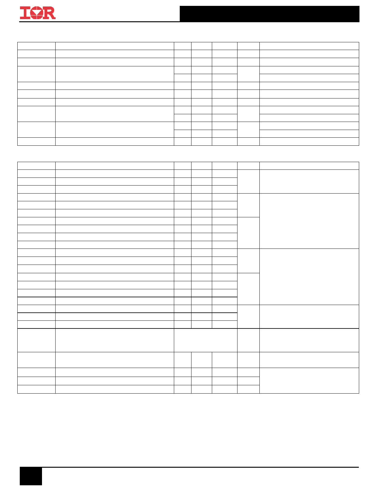
Fig. 3 - Power Dissipation vs.
Case Temperature
0.1
1
10
100
f , Frequency ( kHz )
20
40
60
80
100
Lo
ad
C
ur
re
nt
(
A
)
For both:
Duty cycle : 50%
Tj = 175°C
Tcase = 100°C
Gate drive as specified
Power Dissipation = 167W
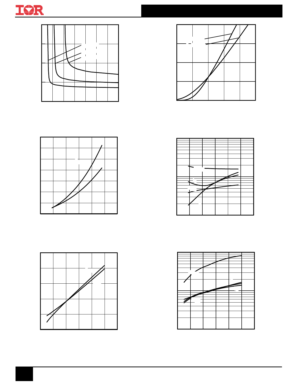
Fig. 1 - Typical Load Current vs. Frequency
(Load Current = I
RMS
of fundamental)
I
Square Wave:
V
CC
Diode as specified
25
50
75
100
125
150
175
TC (°C)
0
20
40
60
80
100
120
I C
(
A
)
Fig. 2 - Maximum DC Collector Current vs.
1
10
100
1000
VCE, Collector-to-Emitter Voltage (V)
0.01
0.1
1
10
100
1000
I C
,
C
ol
le
ct
or
-t
o
-E
m
itt
er
C
ur
re
nt
(
A
)
Tc = 25°C
Tj = 175°C
Single Pulse
1msec
10msec
OPERATION IN THIS AREA
LIMITED BY V CE(on)
100µsec
DC
Fig. 4 - Forward SOA
T
C
= 25°C, T
J
@ 175°C; V
GE
=15V
IRGP4063D1PbF/IRGP4063D1-EPbF
4
www.irf.com
© 2013 International Rectifier
June 24, 2013
0
2
4
6
8
10
VCE (V)
0
50
100
150
200
I C
E
(
A
)
VGE = 18V
VGE = 15V
VGE = 12V
VGE = 10V
VGE = 8.0V
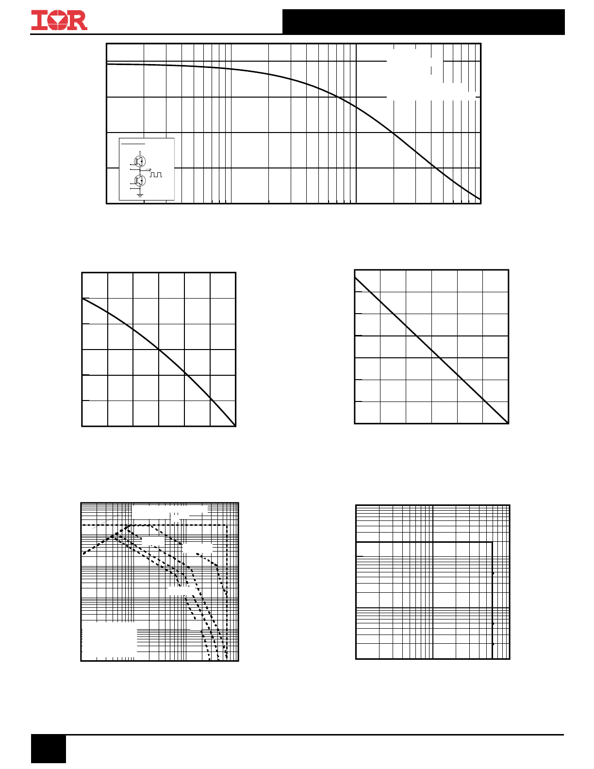
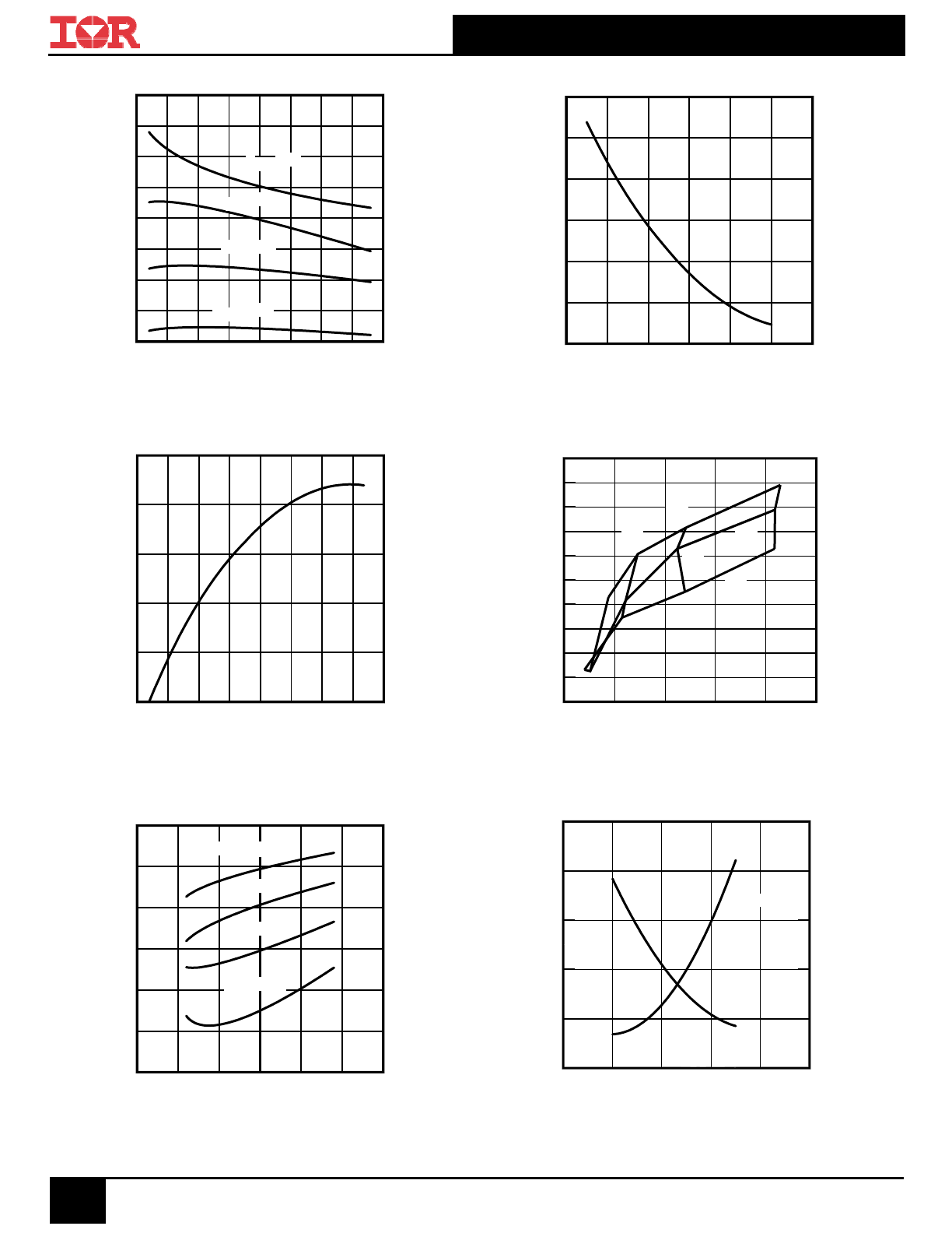
Fig. 7 - Typ. IGBT Output Characteristics
T
J
= 25°C; tp = 20µs
0
2
4
6
8
10
VCE (V)
0
50
100
150
200
I C
E
(
A
)
VGE = 18V
VGE = 15V
VGE = 12V
VGE = 10V
VGE = 8.0V
Fig. 6 - Typ. IGBT Output Characteristics
T
J
= -40°C; tp = 20µs
0
2
4
6
8
10
VCE (V)
0
50
100
150
200
I C
E
(
A
)
VGE = 18V
VGE = 15V
VGE = 12V
VGE = 10V
VGE = 8.0V
0.0
1.0
2.0
3.0
4.0
5.0
6.0
VF (V)
0
50
100
150
200
I F
(
A
)
TJ =175°C
TJ = 25°C
TJ = -40°C
6
8
10
12
14
16
18
20
VGE (V)
0
2
4
6
8
V
C
E
(
V
)
ICE = 24A
ICE = 48A
ICE = 96A
Fig. 8 - Typ. IGBT Output Characteristics
T
J
= 175°C; tp = 20µs
Fig. 10 - Typical V
CE
vs. V
GE
T
J
= -40°C
6
8
10
12
14
16
18
20
VGE (V)
0
2
4
6
8
V
C
E
(
V
)
ICE = 24A
ICE = 48A
ICE = 96A
Fig. 9 - Typ. Diode Forward Characteristics
tp = 20µs
Fig. 111 - Typical V
CE
vs. V
GE
T
J
= 25°C
IRGP4063D1PbF/IRGP4063D1-EPbF
5
www.irf.com
© 2013 International Rectifier
June 24, 2013
6
8
10
12
14
16
VGE, Gate-to-Emitter Voltage (V)
0
50
100
150
200
I C
, C
ol
le
ct
o
r-
to
-E
m
itt
er
C
ur
re
nt
(A
)
TJ = 25°C
TJ = 175°C
6
8
10
12
14
16
18
20
VGE (V)
0
2
4
6
8
V
C
E
(
V
)
ICE = 24A
ICE = 48A
ICE = 96A
0
20
40
60
80
100
120
IC (A)
10
100
1000
S
w
ic
h
in
g
T
im
e
(n
s)
tR
tdOFF
tF
tdON
Fig. 13 - Typ. Transfer Characteristics
V
CE
= 50V; tp = 20µs
Fig. 15 - Typ. Switching Time vs. IC
TJ = 175°C; L = 485µH; V
CE
= 400V, R
G
= 10
; V
GE
= 15V
Fig. 16 - Typ. Energy Loss vs. R
G
T
J
= 175°C; L = 485µH; V
CE
= 400V, I
CE
= 48A; V
GE
= 15V
0
20
40
60
80
100
120
RG ()
10
100
1000
S
w
ic
hi
ng
T
im
e
(n
s)
tR
tdOFF
tF
tdON
Fig. 17 - Typ. Switching Time vs. R
G
T
J
= 175°C; L = 485µH; V
CE
= 400V, I
CE
= 48A; V
GE
= 15V
0
20
40
60
80
100
120
IC (A)
0
1
2
3
4
5
6
7
E
ne
rg
y
(m
J)
EOFF
EON
Fig. 14 - Typ. Energy Loss vs. I
C
T
J
= 175°C; L = 485µH; V
CE
= 400V, R
G
= 10
; V
GE
= 15V
Fig. 12 - Typical V
CE
vs. V
GE
T
J
= 175°C
0
20
40
60
80
100
120
RG ()
1
2
3
4
5
6
E
ne
rg
y
(m
J)
EOFF
EON
IRGP4063D1PbF/IRGP4063D1-EPbF
6
www.irf.com
© 2013 International Rectifier
June 24, 2013
20
30
40
50
60
70
80
90 100
IF (A)
10
12
14
16
18
20
22
24
26
I R
R
(
A
)
RG = 22
RG = 47
RG = 10
RG = 100
0
20
40
60
80
100
120
RG (
)
10
12
14
16
18
20
22
I R
R
(
A
)
300 400 500 600 700 800 900 1000 1100
diF /dt (A/µs)
12
14
16
18
20
22
I R
R
(
A
)
Fig. 18 - Typ. Diode I
RR
vs. I
F
T
J
= 175°C
Fig. 20 - Typ. Diode I
RR
vs. diF/dt
V
CC
= 400V; V
GE
= 15V; I
F
= 48A; T
J
= 175°C
200
400
600
800
1000
1200
diF /dt (A/µs)
600
700
800
900
1000
1100
1200
1300
1400
1500
1600
Q
R
R
(
nC
)
48A
24A
96A
Fig. 19 - Typ. Diode I
RR
vs. R
G
T
J
= 175°C
Fig. 21 - Typ. Diode Q
RR
vs. diF/dt
V
CC
= 400V; V
GE
= 15V; T
J
= 175°C
0
20
40
60
80
100
120
IF (A)
0
50
100
150
200
250
300
E
ne
rg
y
(µ
J)
RG =10
RG = 22
RG = 47
RG = 100
Fig. 22 - Typ. Diode E
RR
vs. I
F
T
J
= 175°C
8
10
12
14
16
18
VGE (V)
0
4
8
12
16
20
T
im
e
(µ
s)
0
200
400
600
800
1000
C
u
rre
n
t (
A
)
Tsc
Isc
Fig. 23 - V
GE
vs. Short Circuit Time
V
CC
= 400V; T
C
= 25°C
IRGP4063D1PbF/IRGP4063D1-EPbF
7
www.irf.com
© 2013 International Rectifier
June 24, 2013
0
100
200
300
400
500
VCE (V)
10
100
1000
10000
C
ap
ac
ita
nc
e
(
pF
)
Cies
Coes
Cres
0
20
40
60
80
100
120
Q G, Total Gate Charge (nC)
0
2
4
6
8
10
12
14
16
18
V
G
E
, G
at
e-
to
-E
m
itt
er
V
ol
ta
ge
(
V
)
VCES = 400V
VCES = 300V
Fig 27. Maximum Transient Thermal Impedance, Junction-to-Case (IGBT)
1E-006
1E-005
0.0001
0.001
0.01
0.1
1
t1 , Rectangular Pulse Duration (sec)
0.0001
0.001
0.01
0.1
1
T
h
er
ma
l R
es
po
ns
e
(
Z t
hJ
C
)
0.20
0.10
D = 0.50
0.02
0.01
0.05
SINGLE PULSE
( THERMAL RESPONSE )
Notes:
1. Duty Factor D = t1/t2
2. Peak Tj = P dm x Zthjc + Tc
Fig. 24 - Typ. Capacitance vs. V
CE
V
GE
= 0V; f = 1MHz
Fig. 25 - Typical Gate Charge vs. V
GE
I
CE
= 48A
Ri (°C/W)
I (sec)
0.0120
0.000012
0.1158
0.00013
0.1820
0.00379
0.1399
0.02387
J
J
1
1
2
2
3
3
R
1
R
1
R
2
R
2
R
3
R
3
Ci=
iRi
Ci=
iRi
C
C
4
4
R
4
R
4
Fig 28. Maximum Transient Thermal Impedance, Junction-to-Case (DIODE)
1E-006
1E-005
0.0001
0.001
0.01
0.1
1
t1 , Rectangular Pulse Duration (sec)
0.001
0.01
0.1
1
10
T
he
rma
l R
es
po
n
se
(
Z
th
JC
)
0.20
0.10
D = 0.50
0.02
0.01
0.05
SINGLE PULSE
( THERMAL RESPONSE )
Notes:
1. Duty Factor D = t1/t2
2. Peak Tj = P dm x Zthjc + Tc
Ri (°C/W)
I (sec)
0.1343
0.00009
0.7058
0.00032
1.0181
0.00327
0.5434
0.03079
J
J
1
1
2
2
3
3
R
1
R
1
R
2
R
2
R
3
R
3
Ci=
iRi
Ci=
iRi
C
C
4
4
R
4
R
4
IRGP4063D1PbF/IRGP4063D1-EPbF
8
www.irf.com
© 2013 International Rectifier
June 24, 2013
L
Rg
80 V
DUT
VCC
+
-
G force
C sense
100K
DUT
0.0075µF
D1
22K
E force
C force
E sense
Fig.C.T.1 - Gate Charge Circuit (turn-off)
Fig.C.T.2 - RBSOA Circuit
Fig.C.T.6 - BVCES Filter Circuit
L
Rg
VCC
DUT /
DRIVER
diode clamp /
DUT
-5V
Rg
VCC
DUT
R =
VCC
ICM
Fig.C.T.4 - Switching Loss Circuit
Fig.C.T.5 - Resistive Load Circuit
DC
4X
DUT
VCC
R
SH
Fig.C.T.3 - S.C. SOA Circuit
IRGP4063D1PbF/IRGP4063D1-EPbF
9
www.irf.com
© 2013 International Rectifier
June 24, 2013
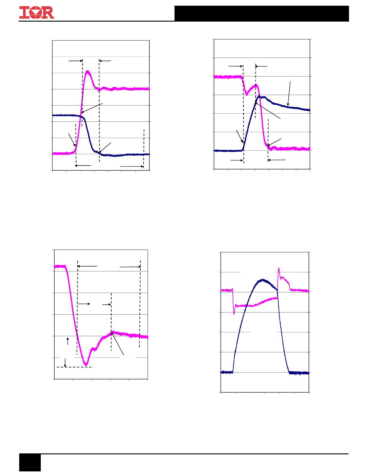
Fig. WF2 - Typ. Turn-on Loss Waveform
@ T
J
= 175°C using Fig. CT.4
Fig. WF3 - Typ. Diode Recovery Waveform
@ T
J
= 175°C using Fig. CT.4
Fig. WF4 - Typ. S.C. Waveform
@ T
J
= 25°C using Fig. CT.3
Fig. WF1 - Typ. Turn-off Loss Waveform
@ T
J
= 175°C using Fig. CT.4
-200
0
200
400
600
800
1000
1200
-100
0
100
200
300
400
500
600
-1
0
1
2
3
4
5
Ic
e (
A
)
Vc
e (
V
)
Time (uS)
V
CE
I
CE
-30
-15
0
15
30
45
60
-1.50 -0.50 0.50
1.50
2.50
3.50
I
F
(A
)
time (µS)
Peak
I
RR
t
RR
Q
RR
10%
Peak
IRR
-20
0
20
40
60
80
100
120
140
-100
0
100
200
300
400
500
600
700
-2
-1
0
1
2
3
4
5
I
CE
(A
)
V
CE
(V
)
time(µs)
90% I
CE
5% V
CE
5% I
CE
Eoff Loss
tf
-20
0
20
40
60
80
100
120
-100
0
100
200
300
400
500
600
-3
-2
-1
0
1
2
3
4
I
CE
(A
)
V
CE
(V
)
time (µs)
TEST
CURRENT
90%
I
CE
5% V
CE
10%
I
CE
tr
Eon Loss
IRGP4063D1PbF/IRGP4063D1-EPbF
10
www.irf.com
© 2013 International Rectifier
June 24, 2013
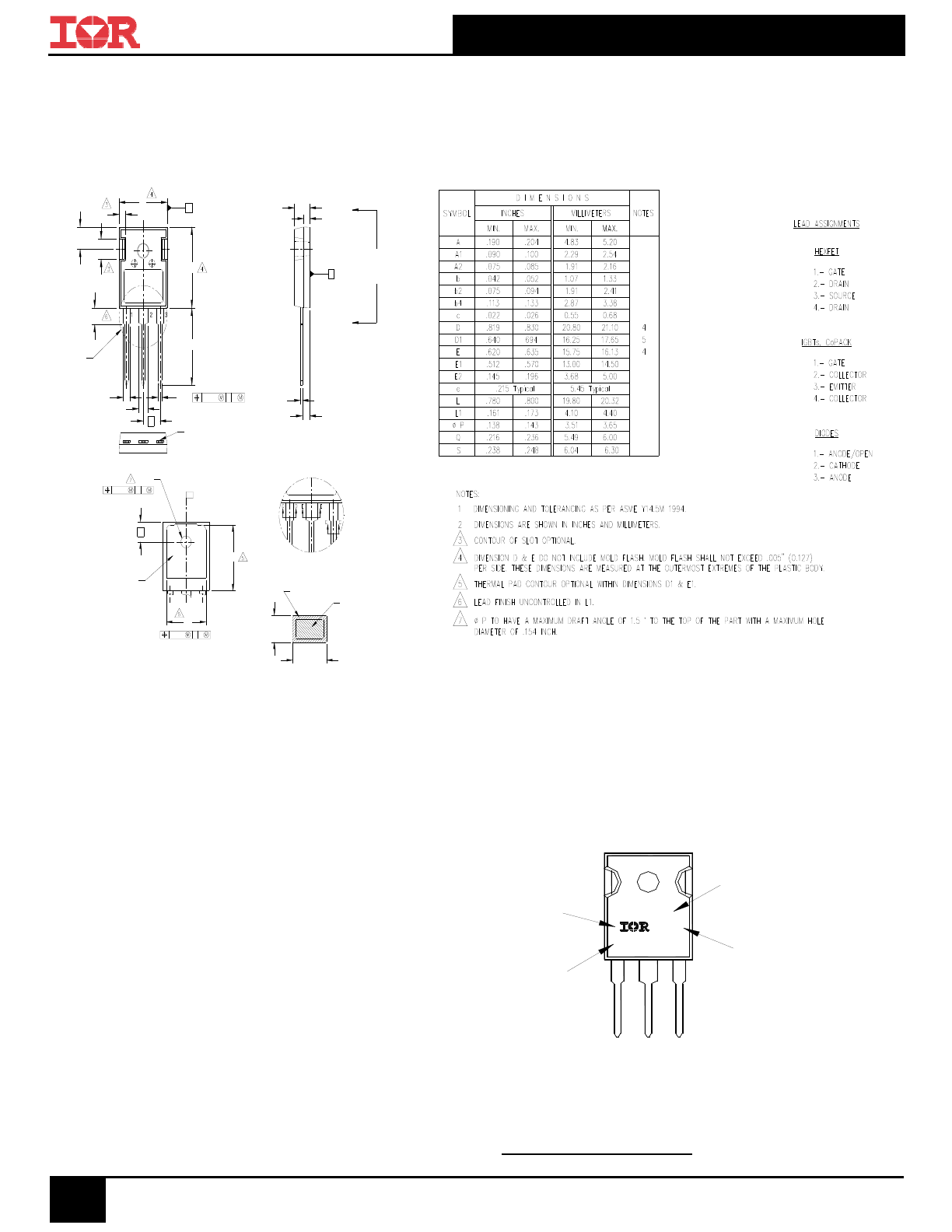
TO-247AC Package Outline
Dimensions are shown in millimeters (inches)
2x
c
"A"
"A"
E
E2/2
Q
E2
2X
L1
L
D
A
e
2x b2
3x b
LEAD TIP
SEE
VIEW "B"
b4
B
A
Ø .010
B A
A2
A1
Ø .010
B A
D1
S
E1
THERMAL PAD
-A-
Ø P
Ø .010
B A
VIEW: "B"
SECTION: C-C, D-D, E-E
(b, b2, b4)
(c)
BASE METAL
PLATING
VIEW: "A" - "A"
YEAR 1 = 2001
DATE CODE
PART NUMBER
INTERNATIONAL
LOGO
RECTIFIER
ASSEMBLY
56 57
IRFPE30
135H
LINE H
indicates "Lead-Free"
WEEK 35
LOT CODE
IN THE ASSEMBLY LINE "H"
ASSEMBLED ON WW 35, 2001
Notes: This part marking information applies to devices produced after 02/26/2001
Note: "P" in assembly line position
EXAMPLE:
WITH ASSEMBLY
THIS IS AN IRFPE30
LOT CODE 5657
TO-247AC Part Marking Information
Note: For the most current drawing please refer to IR website at http://www.irf.com/package/
TO-247AC package is not recommended for Surface Mount Application.