
www.irf.com
1
02/29/12
IRFTS9342PbF
HEXFET
®
Power MOSFET
Notes
through
are on page 2
Applications
l
Battery operated DC motor inverter MOSFET
l
System/Load Switch
Features and Benefits
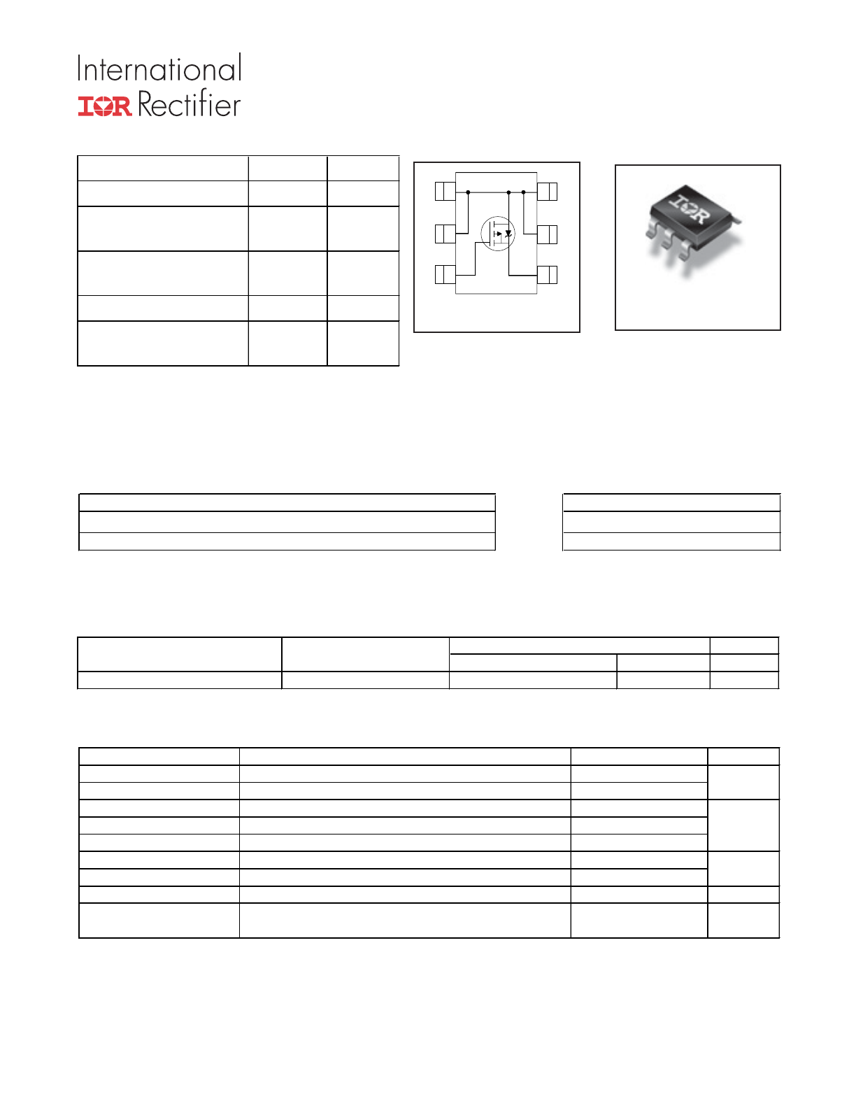
Top View
1
2
D
G
A
D
D
D
S
3
4
5
6
TSOP-6
V
DS
-30
V
V
GS max
±20
V
R
DS(on) max
(@V
GS
= -10V)
40
m
Ω
R
DS(on) max
(@V
GS
= -4.5V)
66
m
Ω
Q
g typ
12
nC
I
D
(@T
A
= 25°C)
-5.8
A
Absolute Maximum Ratings
Parameter
Units
V
DS
Drain-to-Source Voltage
V
GS
Gate-to-Source Voltage
I
D
@ T
A
= 25°C
Continuous Drain Current, V
GS
@ 4.5V
I
D
@ T
A
= 70°C
Continuous Drain Current, V
GS
@ 4.5V
I
DM
Pulsed Drain Current
c
P
D
@T
A
= 25°C
Power Dissipation
P
D
@T
A
= 70°C
Power Dissipation
Linear Derating Factor
W/°C
T
J
Operating Junction and
T
STG
Storage Temperature Range
V
W
A
°C
Max.
-5.8
-46
±20
-30
-4.6
-55 to + 150
2.0
0.02
1.3
Note
Form
Quantity
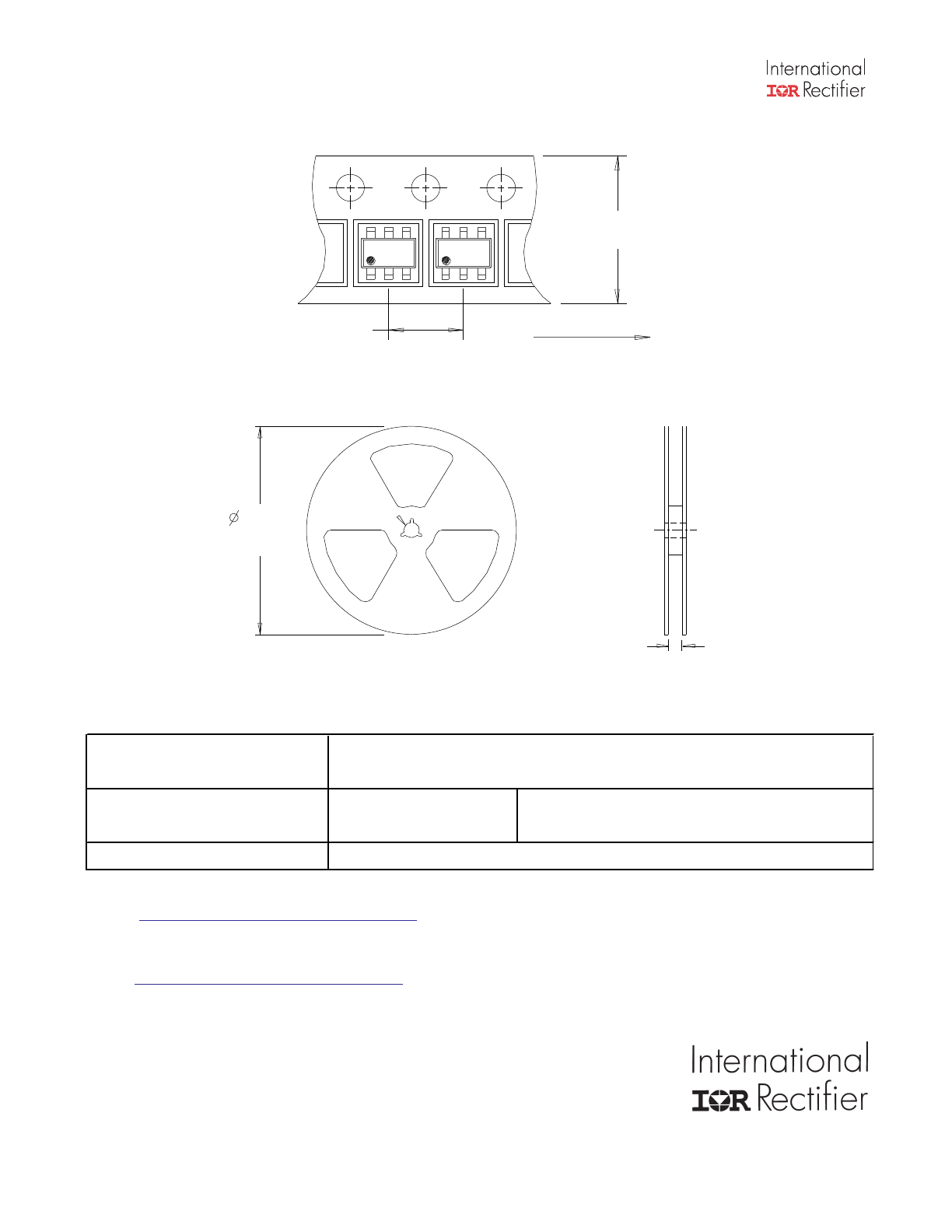
IRFTS9342TRPbF
TSOP-6
Tape and Reel
3000
Orderable part number
Package Type
Standard Pack
Features
Benefits
Industry-Standard TSOP-6 Package
results in Multi-Vendor Compatibility
RoHS Compliant Containing no Lead, no Bromide and no Halogen
⇒
Environmentally Friendlier
MSL1, Consumer Qualification
Increased Reliability
PD - 96411A
IRFTS9342PbF
2
www.irf.com
G
D
S
Notes:
Repetitive rating; pulse width limited by max. junction temperature.
Pulse width
≤ 400μs; duty cycle ≤ 2%.
When mounted on 1 inch square copper board.
Thermal Resistance
Parameter
Typ.
Max.
Units
R
θJA
Junction-to-Ambient
e
–––
62.5
°C/W
Static @ T
J
= 25°C (unless otherwise specified)
Parameter
Min. Typ. Max. Units
BV
DSS
Drain-to-Source Breakdown Voltage
-30
–––
–––
V
ΔΒV
DSS
/
ΔT
J
Breakdown Voltage Temp. Coefficient
–––
19
––– mV/°C
R
DS(on)
Static Drain-to-Source On-Resistance
–––
32
40
–––
53
66
V
GS(th)
Gate Threshold Voltage
-1.3
–––
-2.4
V
ΔV
GS(th)
Gate Threshold Voltage Coefficient
–––
-5.5
––– mV/°C
I
DSS
Drain-to-Source Leakage Current
–––
–––
-1.0
–––
–––
-150
I
GSS
Gate-to-Source Forward Leakage
–––
–––
-100
Gate-to-Source Reverse Leakage
–––
–––
100
gfs
Forward Transconductance
6.8
–––
–––
S
Q
g
Total Gate Charge
–––
12
–––
Q
gs
Gate-to-Source Charge
–––
1.8
–––
Q
gd
Gate-to-Drain Charge
–––
3.1
–––
R
G
Gate Resistance
–––
17
–––
Ω
t
d(on)
Turn-On Delay Time
–––
4.6
–––
t
r
Rise Time
–––
13
–––
t
d(off)
Turn-Off Delay Time
–––
45
–––
t
f
Fall Time
–––
28
–––
C
iss
Input Capacitance
–––
595
–––
C
oss
Output Capacitance
–––
133
–––
C
rss
Reverse Transfer Capacitance
–––
85
–––
Diode Characteristics
Parameter
Min. Typ. Max. Units
I
S
Continuous Source Current
(Body Diode)
I
SM
Pulsed Source Current
(Body Diode)
c
V
SD
Diode Forward Voltage
–––
–––
-1.2
V
t
rr
Reverse Recovery Time
–––
20
30
ns
Q
rr
Reverse Recovery Charge
–––
11
17
nC
t
on
Forward Turn-On Time
Time is dominated by parasitic Inductance
V
DS
= V
GS
, I
D
= -25μA
V
GS
= -4.5V, I
D
= -4.6A
e
m
Ω
V
DD
= -15V, V
GS
= -10V
V
DS
= -15V
R
G
= 6.8
Ω
V
DS
= -10V, I
D
= -4.6A
V
DS
= -24V, V
GS
= 0V, T
J
= 125°C
μA
I
D
= -4.6A
I
D
= -4.6A
V
GS
= 0V
V
DS
= -25V
V
DS
= -24V, V
GS
= 0V
T
J
= 25°C, I
F
= -4.6A, V
DD
= -24V
di/dt = 100A/μs
e
T
J
= 25°C, I
S
= -4.6A, V
GS
= 0V
e
showing the
integral reverse
p-n junction diode.
Conditions
ƒ = 1.0KHz
Conditions
V
GS
= 0V, I
D
= -250μA
Reference to 25°C, I
D
= -1mA
V
GS
= -10V, I
D
= -5.8A
e
–––
–––
-46
–––
–––
-2.0
MOSFET symbol
nA
ns
A
pF
nC
V
GS
= -10V
V
GS
= -20V
V
GS
= 20V
IRFTS9342PbF
www.irf.com
3
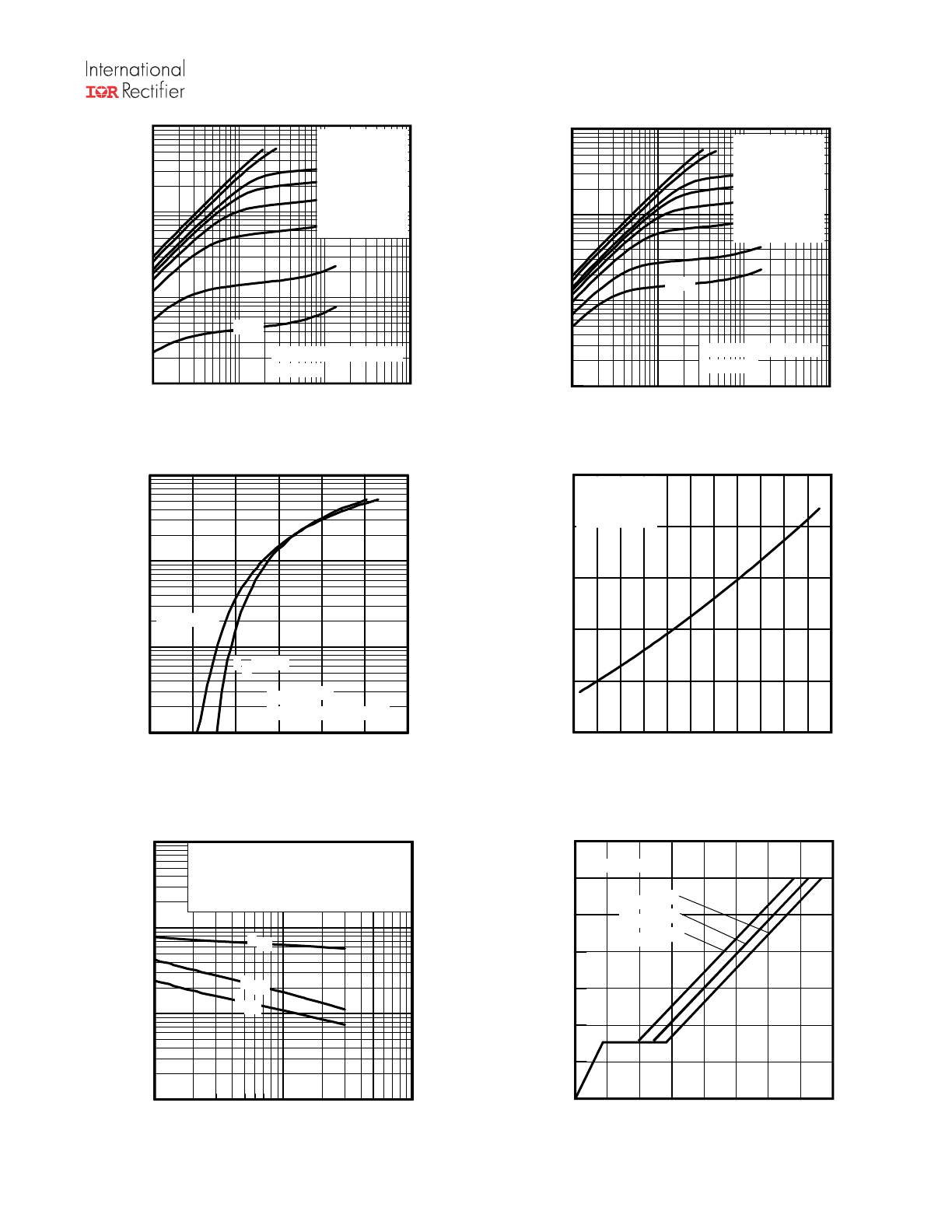
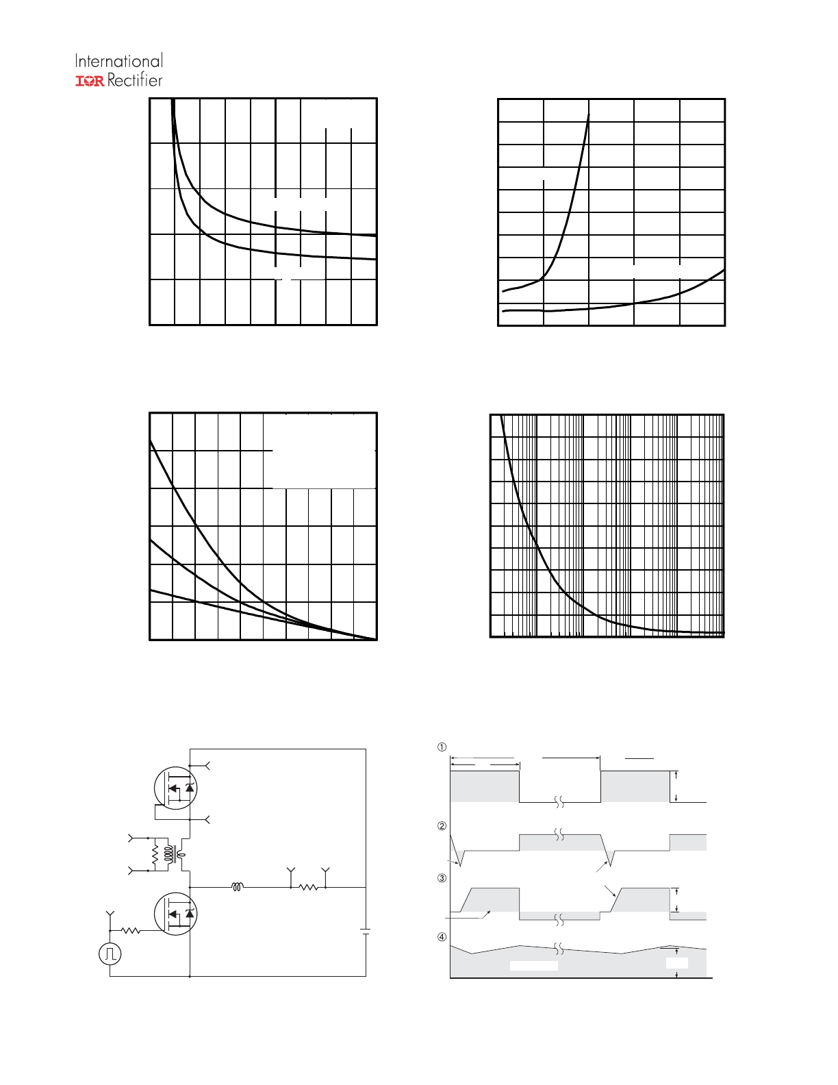
Fig 4. Normalized On-Resistance vs. Temperature
Fig 2. Typical Output Characteristics
Fig 1. Typical Output Characteristics
Fig 3. Typical Transfer Characteristics
Fig 6. Typical Gate Charge vs.Gate-to-Source Voltage
Fig 5. Typical Capacitance vs.Drain-to-Source Voltage
-60 -40 -20 0 20 40 60 80 100 120 140 160
TJ , Junction Temperature (°C)
0.6
0.8
1.0
1.2
1.4
1.6
R
D
S
(o
n)
,
D
ra
in
-t
o-
S
ou
rc
e
O
n
R
es
is
ta
nc
e
(
N
or
m
al
iz
ed
)
ID = -5.8A
VGS = -10V
1
10
100
-VDS, Drain-to-Source Voltage (V)
10
100
1000
10000
C
, C
ap
ac
ita
nc
e
(p
F
)
VGS = 0V, f = 1 MHZ
Ciss = Cgs + Cgd, C ds SHORTED
Crss = Cgd
Coss = Cds + Cgd
Coss
Crss
Ciss
0
2
4
6
8
10
12
14
16
QG Total Gate Charge (nC)
0.0
2.0
4.0
6.0
8.0
10.0
12.0
14.0
-V
G
S
, G
at
e-
to
-S
ou
rc
e
V
ol
ta
ge
(
V
)
VDS= -24V
VDS= -15V
VDS= -6.0V
ID= -4.6A
0.1
1
10
100
-V DS, Drain-to-Source Voltage (V)
0.1
1
10
100
-I D
, D
ra
in
-t
o-
S
ou
rc
e
C
ur
re
nt
(
A
)
VGS
TOP
-10V
-7.0V
-5.0V
-4.5V
-4.0V
-3.5V
-3.0V
BOTTOM
-2.8V
≤60μs PULSE WIDTH
Tj = 25°C
-2.8V
0.1
1
10
100
-VDS, Drain-to-Source Voltage (V)
0.1
1
10
100
-I D
, D
ra
in
-t
o-
S
ou
rc
e
C
ur
re
nt
(
A
)
-2.8V
≤60μs PULSE WIDTH
Tj = 150°C
VGS
TOP
-10V
-7.0V
-5.0V
-4.5V
-4.0V
-3.5V
-3.0V
BOTTOM
-2.8V
1
2
3
4
5
6
7
-VGS, Gate-to-Source Voltage (V)
0.1
1
10
100
-I
D
, D
ra
in
-t
o-
S
ou
rc
e
C
ur
re
nt
(
A
)
TJ = 25°C
TJ = 150°C
VDS = -15V
≤60μs PULSE WIDTH
IRFTS9342PbF
4
www.irf.com
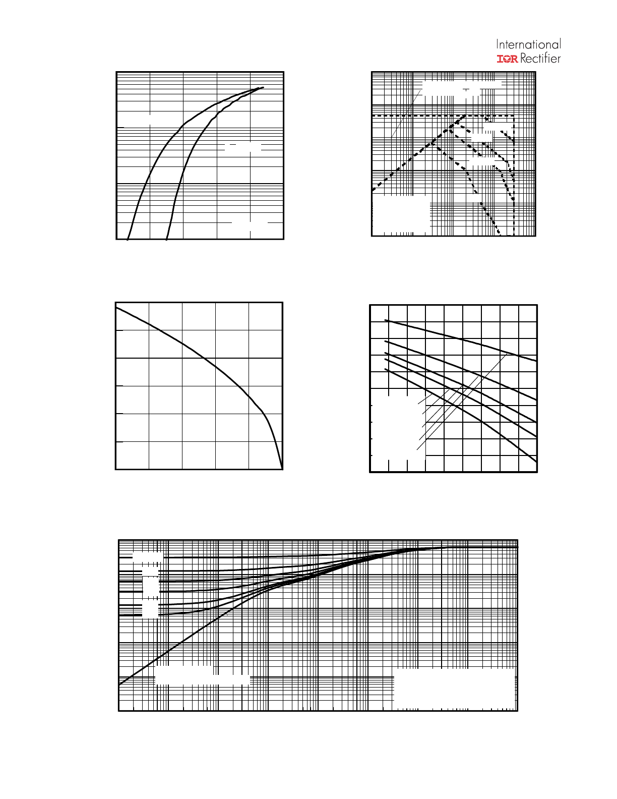
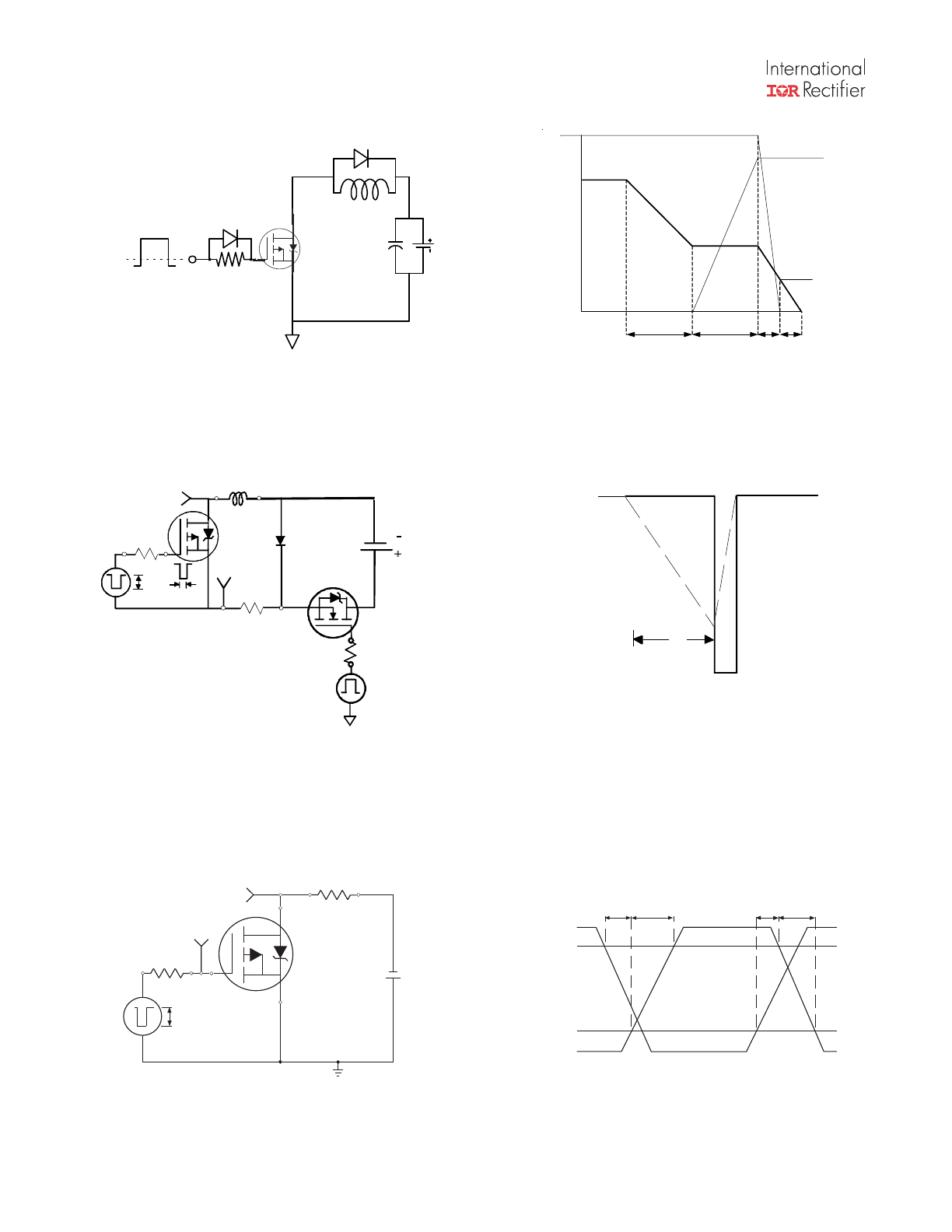
Fig 11. Maximum Effective Transient Thermal Impedance, Junction-to-Case
Fig 8. Maximum Safe Operating Area
Fig 9. Maximum Drain Current vs.
Case Temperature
Fig 7. Typical Source-Drain Diode Forward Voltage
Fig 10. Threshold Voltage vs. Temperature
25
50
75
100
125
150
TA , Ambient Temperature (°C)
0
1
2
3
4
5
6
-I
D
,
D
ra
in
C
ur
re
nt
(
A
)
1E-006
1E-005
0.0001
0.001
0.01
0.1
1
10
100
t1 , Rectangular Pulse Duration (sec)
0.001
0.01
0.1
1
10
100
T
he
rm
al
R
es
po
ns
e
(
Z
th
JA
)
°C
/W
0.20
0.10
D = 0.50
0.02
0.01
0.05
SINGLE PULSE
( THERMAL RESPONSE )
Notes:
1. Duty Factor D = t1/t2
2. Peak Tj = P dm x Zthja + TA
0.01
0.1
1
10
100
VDS, Drain-to-Source Voltage (V)
0.01
0.1
1
10
100
1000
I D
,
D
ra
in
-t
o-
S
ou
rc
e
C
ur
re
nt
(
A
)
Tc = 25°C
Tj = 150°C
Single Pulse
1msec
10msec
OPERATION IN THIS AREA
LIMITED BY RDS(on)
100μsec
DC
0.4
0.6
0.8
1.0
1.2
1.4
-VSD, Source-to-Drain Voltage (V)
0.1
1
10
100
-I
S
D
, R
ev
er
se
D
ra
in
C
ur
re
nt
(
A
)
TJ = 25°C
TJ = 150°C
VGS = 0V
-75 -50 -25
0
25
50
75 100 125 150
TJ , Temperature ( °C )
1.0
1.2
1.4
1.6
1.8
2.0
2.2
2.4
2.6
2.8
3.0
-V
G
S
(t
h)
, G
at
e
th
re
sh
ol
d
V
ol
ta
ge
(
V
)
ID = -25μA
ID = -250μA
ID = -1.0mA
ID = -10mA
ID = -1.0A
IRFTS9342PbF
www.irf.com
5
Fig 12. On-Resistance vs. Gate Voltage
Fig 13. Typical On-Resistance vs. Drain Current
Fig 14. Maximum Avalanche Energy vs. Drain Current
Fig 15
. Typical Power vs. Time
*
Reverse Polarity of D.U.T for P-Channel
P.W.
Period
di/dt
Diode Recovery
dv/dt
Ripple
≤ 5%
Body Diode Forward Drop
Re-Applied
Voltage
Reverse
Recovery
Current
Body Diode Forward
Current
V
GS
=10V
V
DD
I
SD
Driver Gate Drive
D.U.T. I
SD
Waveform
D.U.T. V
DS
Waveform
Inductor Curent
D =
P.W.
Period
*
V
GS
= 5V for Logic Level Devices
*
Inductor Current
Circuit Layout Considerations
• Low Stray Inductance
• Ground Plane
• Low Leakage Inductance
Current Transformer
• di/dt controlled by R
G
• Driver same type as D.U.T.
• I
SD
controlled by Duty Factor "D"
• D.U.T. - Device Under Test
+
-
+
+
+
-
-
-
R
G
V
DD
D.U.T
*
Fig 16.
Diode Reverse Recovery Test Circuit for P-Channel HEXFET
®
Power MOSFETs
2
4
6
8
10
12
14
16
18
20
-VGS, Gate -to -Source Voltage (V)
0
20
40
60
80
100
R
D
S
(o
n)
,
D
ra
in
-t
o
-S
ou
rc
e
O
n
R
es
is
ta
nc
e
(m
Ω
)
ID = -5.8A
TJ = 25°C
TJ = 125°C
0
10
20
30
40
50
-ID, Drain Current (A)
20
40
60
80
100
120
140
160
180
200
220
R
D
S
(o
n)
,
D
ra
in
-t
o
-S
ou
rc
e
O
n
R
es
is
ta
nc
e
(m
Ω
)
Vgs = -4.5V
Vgs = -10V
25
50
75
100
125
150
Starting TJ , Junction Temperature (°C)
0
20
40
60
80
100
120
E
A
S
,
S
in
gl
e
P
ul
se
A
va
la
nc
he
E
ne
rg
y
(m
J)
ID
TOP -0.91A
-1.4A
BOTTOM -4.6A
0.0001
0.001
0.01
0.10
1
10
Time (sec)
0
10
20
30
40
50
60
70
80
90
100
P
ow
er
(
W
)
IRFTS9342PbF
6
www.irf.com
Fig 17a. Gate Charge Test Circuit
Fig 17b. Gate Charge Waveform
Fig 18b. Unclamped Inductive Waveforms
Fig 18a. Unclamped Inductive Test Circuit
Fig 19b. Switching Time Waveforms
Fig 19a. Switching Time Test Circuit
Vds
Vgs
Id
Vgs(th)
Qgs1
Qgs2
Qgd
Qgodr
1K
VCC
DUT
0
L
S
20K
S
RG
IAS
0.01Ω
tp
D.U.T
L
V
DS
VDD
DRIVER
A
15V
-20V
-V
GS
V
DS
-V
GS
Pulse Width ≤ 1 µs
Duty Factor ≤ 0.1 %
R
D
V
GS
V
DD
R
G
D.U.T.
+
-
tp
V
(BR)DSS
I
AS
V
DS
90%
10%
V
GS
t
d(on)
t
r
t
d(off)
t
f
IRFTS9342PbF
www.irf.com
7
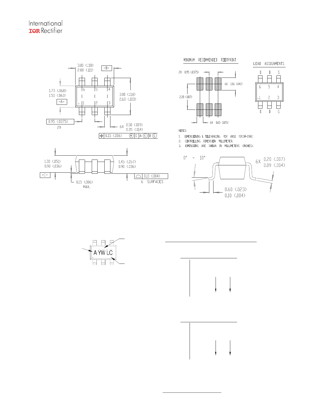
Note: For the most current drawing please refer to IR website at: http://www.irf.com/package/
TSOP-6 Package Outline
TSOP-6 Part Marking Information
WW = (27-52) IF PRECEDED BY A LETTER
C
H
K
J
E
F
G
D
0
2010
YEAR
B
A
Y
2007
2008
2009
2006
2005
2003
2004
2001
2002
5
7
9
8
6
3
4
1
2
C
29
Z
52
50
51
X
Y
30
D
X
24
W
WORK
WEEK
27
28
B
A
26
25
Z
Y
03
04
01
02
C
D
A
B
DATE CODE MARKING INSTRUCTIONS
WW = (1-26) IF PRECEDED BY LAST DIGIT OF CALENDAR YEAR
YEAR
Y
W
WEEK
WORK
2020
2017
2018
2019
2016
2015
2013
2014
2011
2012
2010
2007
2008
2009
2006
2005
2003
2004
2001
2002
2020
2017
2018
2019
2016
2015
2013
2014
2011
2012
CODE
TOP
PART NUMBER
W = WEEK
Y = YEAR
LOT
F = IRF5801
(as shown here) indicates Lead-Free.
Note: A line above the work week
A = S I3443DV
B = IRF5800
G = IRF5803
D = IRF5851
E = IRF5852
I = IRF5805
C = IRF5850
N = IRF5802
K = IRF5810
PART NUMBER CODE REFERENCE:
J = IRF5806
H = IRF5804
O = IRLTS6342TRPBF
P = IRFTS 8342T RPBF
S = Not applicable
R = IRFTS 9342TRPBF
T = IRLT S2242TRPBF
IRFTS9342PbF
8
www.irf.com
TSOP-6 Tape and Reel Information
†
Qualification standards can be found at International Rectifier’s web site
http://www.irf.com/product-info/reliability
††
Higher qualification ratings may be available should the user have such requirements.
Please contact your International Rectifier sales representative for further information:
http://www.irf.com/whoto-call/salesrep/
†††
Applicable version of JEDEC standard at the time of product release.
IR WORLD HEADQUARTERS: 101 N. Sepulveda Blvd., El Segundo, California 90245, USA Tel: (310) 252-7105
TAC Fax: (310) 252-7903
Visit us at www.irf.com for sales contact information. 02/2012
Data and specifications subject to change without notice.
8mm
FEED DIRECTION
4mm
NOTES :
1. OUTLINE CONFORMS TO EIA-481 & EIA-541.
9.90 ( .390 )
8.40 ( .331 )
178.00
( 7.008 )
MAX.
NOTES:
1. CONTROLLING DIMENSION : MILLIMETER.
2. OUTLINE CONFORMS TO EIA-481 & EIA-541.
MS L1
(per IPC/JE DEC J-S T D-020D
†††
)
RoHS compliant
Yes
TSOP-6
Qualification information
†
Moisture Sensitivity Level
Qualification level
Consumer
††
(per JEDE C JE S D47F
†††
guidelines )