
IRFS4321-7PPbF
1
www.irf.com
© 2013 International Rectifier
June 14, 2013
HEXFET
®
Power MOSFET
D
S
G
D
2
Pak 7Pin
G D S
Gate Drain Source
Application
Motion Control Applications
High Efficiency Synchronous Rectification in SMPS
Uninterruptible Power Supply
Hard Switched and High Frequency Circuits
Benefits
Low Rdson Reduces Losses
Low Gate Charge Improves the Switching Performance
Improved Diode Recovery Improves Switching &
EMI Performance
30V Gate Voltage Rating Improves Robustness
Fully Characterized Avalanche SOA
V
DSS
150V
R
DS(on) typ.
11.7m
max
14.7m
I
D
86A
Parameter Max.
Units
I
D
@ T
C
= 25°C
Continuous Drain Current, V
GS
@ 10V
86
A
I
D
@ T
C
= 100°C
Continuous Drain Current, V
GS
@ 10V
61
I
DM
Pulsed Drain Current
343
P
D
@T
C
= 25°C
Maximum Power Dissipation
350
W
Linear Derating Factor
2.3
W/°C
V
GS
Gate-to-Source Voltage
± 30
V
E
AS (Thermally limited)
Single Pulse Avalanche Energy
120 mJ
T
J
T
STG
Operating Junction and
Storage Temperature Range
-55 to + 175
°C
Soldering Temperature, for 10 seconds
(1.6mm from case)
300
Thermal Resistance
Parameter Typ.
Max.
Units
R
JC
Junction-to-Case
––– 0.43*
°C/W
R
JA
Junction-to-Ambient
––– 40
Base part number Package Type
Standard Pack
Orderable Part Number
Form
Quantity
IRFS4321-7PPbF
D
2
Pak-7Pin
Tube
50
IRFS4321-7PPbF
Tape and Reel Left
800
IRFS4321TRL7PP
R
JC
(end of life) for D2Pak and TO-262 = 0.65°C/W. This is the maximum measured value after 1000 temperature
cycles from -55 to 150°C and is accounted for by the physical wear out of the die attach medium.
Notes through
are on page 2
IRFS4321-7PPbF
2
www.irf.com
© 2013 International Rectifier
June 14, 2013
Static @ T
J
= 25°C (unless otherwise specified)
Parameter Min.
Typ.
Max.
Units
Conditions
V
(BR)DSS
Drain-to-Source Breakdown Voltage
150
––– –––
V
V
GS
= 0V, I
D
= 250µA
V
(BR)DSS
/
T
J
Breakdown Voltage Temp. Coefficient
–––
150 ––– mV/°C Reference to 25°C, I
D
= 1mA
R
DS(on)
Static Drain-to-Source On-Resistance
––– 11.7 14.7
m
V
GS
= 10V, I
D
= 34A
V
GS(th)
Gate Threshold Voltage
3.0
––– 5.0
V
V
DS
= V
GS
, I
D
= 250µA
I
DSS
Drain-to-Source Leakage Current
––– ––– 20 µA V
DS
=150 V, V
GS
= 0V
––– ––– 1.0 mA V
DS
=150V,V
GS
= 0V,T
J
=125°C
I
GSS
Gate-to-Source Forward Leakage
–––
––– 100
nA
V
GS
= 20V
Gate-to-Source Reverse Leakage
–––
––– -100
V
GS
= -20V
R
G(int)
Internal Gate Resistance
–––
0.8
–––
Dynamic Electrical Characteristics @ T
J
= 25°C (unless otherwise specified)
gfs Forward
Transconductance
130
–––
–––
S
V
DS
= 25V, I
D
=50A
Q
g
Total Gate Charge
–––
71
110
nC
I
D
= 50A
Q
gs
Gate-to-Source Charge
–––
24
V
DS
= 75V
Q
gd
Gate-to-Drain (“Miller”) Charge
–––
21
V
GS
= 10V
t
d(on)
Turn-On Delay Time
–––
18
–––
ns
V
DD
= 98V
t
r
Rise Time
–––
60
–––
I
D
= 50A
t
d(off)
Turn-Off Delay Time
–––
25
–––
R
G
= 2.5
t
f
Fall Time
–––
35
–––
V
GS
= 10V
C
iss
Input Capacitance
––– 4460 –––
V
GS
= 0V
C
oss
Output Capacitance
–––
390 –––
pF V
DS
= 50V
C
rss
Reverse Transfer Capacitance
–––
82
–––
ƒ = 1.0MHz
Diode Characteristics
Parameter
Min. Typ. Max. Units
Conditions
I
S
Continuous Source Current
––– ––– 86
A
MOSFET symbol
(Body Diode)
showing the
I
SM
Pulsed Source Current
––– ––– 343
integral reverse
(Body Diode)
p-n junction diode.
V
SD
Diode Forward Voltage
–––
––– 1.3
V
T
J
= 25°C,I
S
= 50A,V
GS
= 0V
t
rr
Reverse Recovery Time
–––
89
130
ns I
F
= 50A,
Q
rr
Reverse Recovery Charge
–––
300 450
nC V
DD
= 128V
I
RRM
Reverse Recovery Current
–––
6.5
–––
A
di/dt = 100A/µs
D
S
G
Notes:
Repetitive rating; pulse width limited by max. junction temperature.
Limited by T
jmax
, starting T
J
= 25°C, L = 0.096mH, R
G
= 25
, I
AS
= 50A, V
GS
=10V. Part not recommended for use above this value.
Pulse width
400µs; duty cycle 2%.
R
is measured at T
J
approximately 90°C
IRFS4321-7PPbF
3
www.irf.com
© 2013 International Rectifier
June 14, 2013
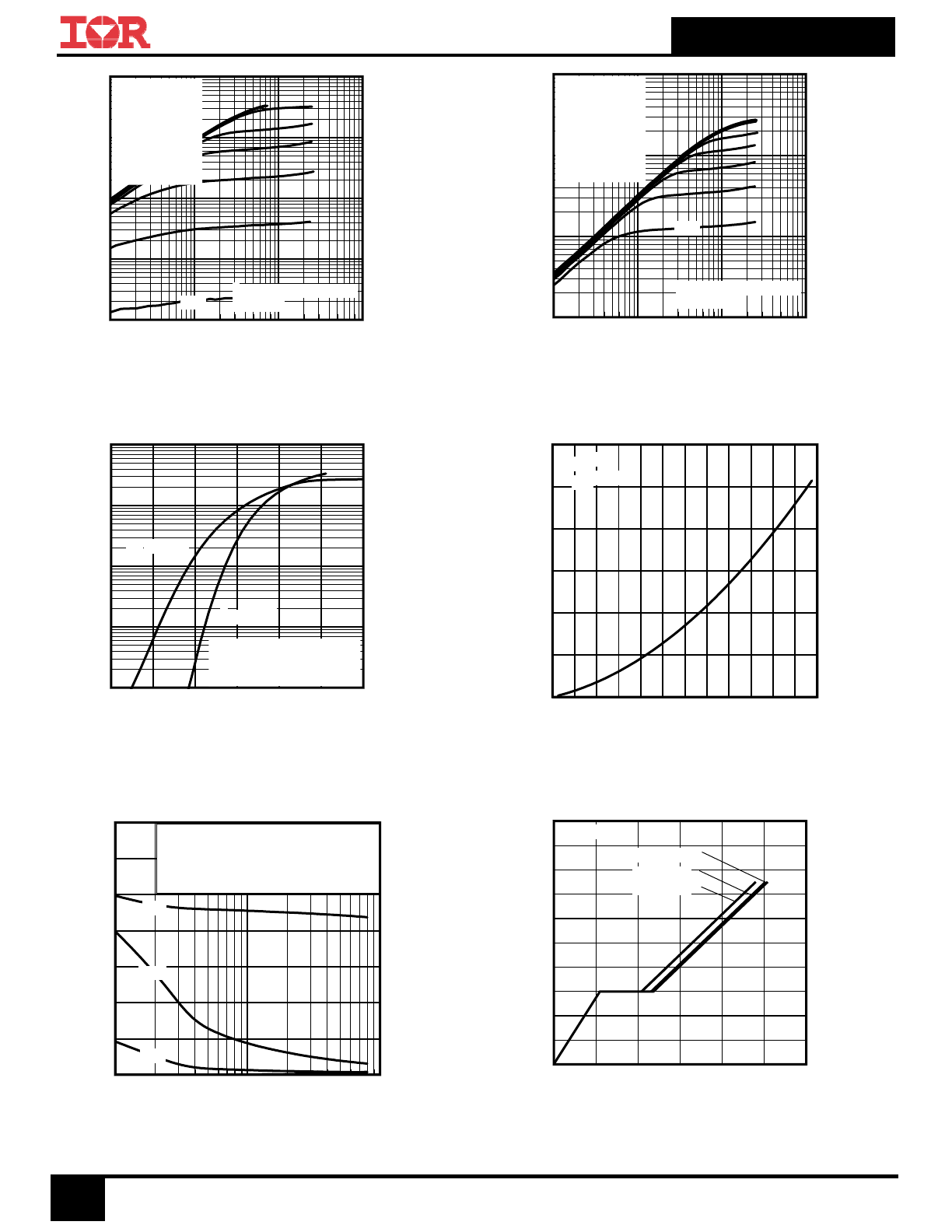
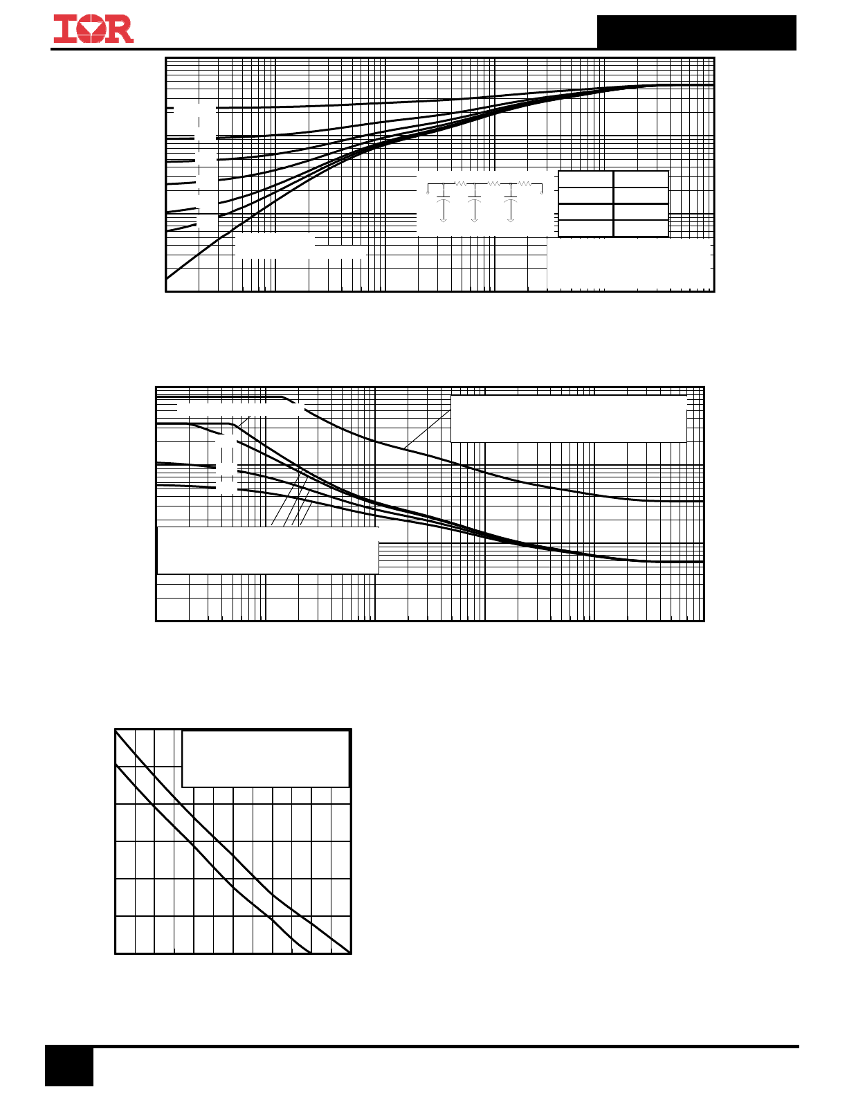
Fig 1. Typical Output Characteristics
Fig 4. Normalized On-Resistance vs. Temperature
Fig 5. Typical Capacitance vs. Drain-to-Source Voltage
Fig 6. Typical Gate Charge vs. Gate-to-Source Voltage
Fig 3. Typical Transfer Characteristics
Fig 2. Typical Output Characteristics
0.1
1
10
100
VDS, Drain-to-Source Voltage (V)
0.1
1
10
100
1000
I D
, D
ra
in
-t
o-
S
ou
rc
e
C
ur
re
nt
(
A
)
60µs PULSE WIDTH
Tj = 25°C
5.0V
VGS
TOP 15V
10V
8.0V
7.0V
6.5V
6.0V
5.5V
BOTTOM
5.0V
0.1
1
10
100
VDS, Drain-to-Source Voltage (V)
1
10
100
1000
I D
, D
ra
in
-t
o-
S
ou
rc
e
C
ur
re
nt
(
A
)
60µs PULSE WIDTH
Tj = 175°C
5.0V
VGS
TOP 15V
10V
8.0V
7.0V
6.5V
6.0V
5.5V
BOTTOM
5.0V
3.0
4.0
5.0
6.0
7.0
8.0
9.0
VGS, Gate-to-Source Voltage (V)
0.1
1
10
100
1000
I D
, D
ra
in
-t
o-
S
ou
rc
e
C
ur
re
nt
)
VDS = 25V
60µs PULSE WIDTH
TJ = 25°C
TJ = 175°C
-60 -40 -20 0
20 40 60 80 100 120 140 160 180
TJ , Junction Temperature (°C)
0.5
1.0
1.5
2.0
2.5
3.0
3.5
R
D
S
(o
n)
,
D
ra
in
-t
o-
S
ou
rc
e
O
n
R
es
is
ta
nc
e
(
N
or
m
al
iz
ed
)
ID = 50A
VGS = 10V
1
10
100
VDS, Drain-to-Source Voltage (V)
0
1000
2000
3000
4000
5000
6000
7000
C
, C
ap
ac
ita
nc
e
(p
F
)
Coss
Crss
Ciss
VGS = 0V, f = 1 MHZ
Ciss = Cgs + Cgd, Cds SHORTED
Crss = Cgd
Coss = Cds + Cgd
0
20
40
60
80
100
120
QG Total Gate Charge (nC)
0
4
8
12
16
20
V
G
S
, G
at
e-
to
-S
ou
rc
e
V
ol
ta
ge
(
V
)
VDS= 120V
VDS= 75V
VDS= 30V
ID= 50A
IRFS4321-7PPbF
4
www.irf.com
© 2013 International Rectifier
June 14, 2013
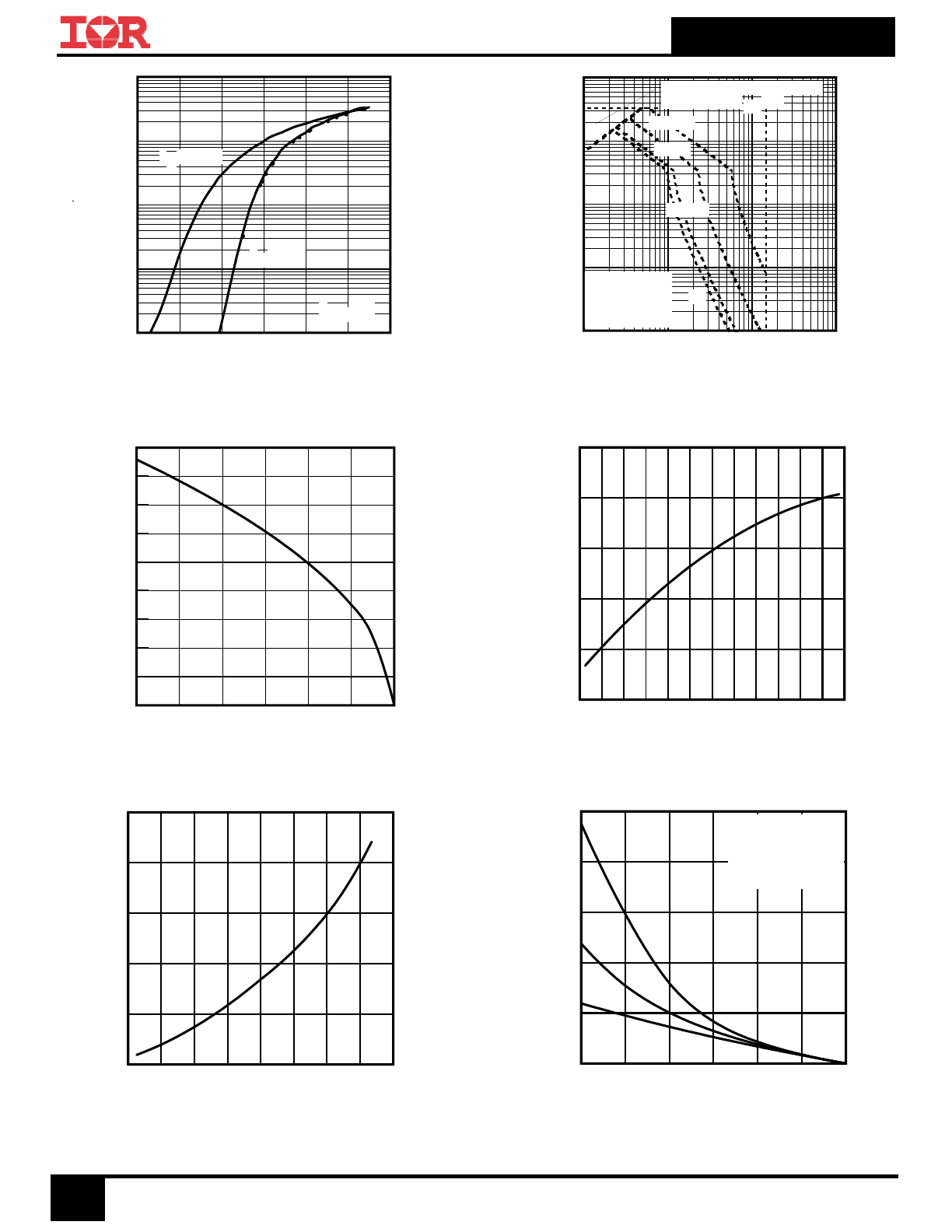
Fig 8. Maximum Safe Operating Area
Fig 11. Typical C
oss
Stored Energy
Fig 12. Maximum Avalanche Energy Vs. Drain Current
Fig 7. Typical Source-Drain Diode Forward Voltage
25
50
75
100
125
150
175
Starting TJ, Junction Temperature (°C)
0
100
200
300
400
500
E
A
S
,
S
in
gl
e
P
ul
se
A
va
la
nc
he
E
ne
rg
y
(m
J)
I D
TOP
13A
20A
BOTTOM
50A
Fig 10. Drain-to–Source Breakdown Voltage
0
20
40
60
80
100
120
140
160
VDS, Drain-to-Source Voltage (V)
0.0
1.0
2.0
3.0
4.0
5.0
E
ne
rg
y
(µ
J)
Fig 9. Maximum Drain Current vs. Case Temperature
0.2
0.4
0.6
0.8
1.0
1.2
1.4
VSD, Source-to-Drain Voltage (V)
0.1
1
10
100
1000
I S
D
, R
ev
er
se
D
ra
in
C
ur
re
nt
(
A
)
TJ = 25°C
TJ = 175°C
VGS = 0V
1
10
100
1000
VDS , Drain-toSource Voltage (V)
0.1
1
10
100
1000
I D
,
D
ra
in
-t
o-
S
ou
rc
e
C
ur
re
nt
(
A
)
Tc = 25°C
Tj = 175°C
Single Pulse
1msec
10msec
OPERATION IN THIS AREA
LIMITED BY R DS(on)
100µsec
DC
-60 -40 -20 0
20 40 60 80 100 120 140 160 180
TJ , Junction Temperature (°C)
140
150
160
170
180
190
V
(B
R
)D
S
S
,
D
ra
in
-t
o-
S
ou
rc
e
B
re
ak
do
w
n
V
ol
ta
ge
25
50
75
100
125
150
175
TC , Case Temperature (°C)
0
10
20
30
40
50
60
70
80
90
I D
,
D
ra
in
C
ur
re
nt
(
A
)
IRFS4321-7PPbF
5
www.irf.com
© 2013 International Rectifier
June 14, 2013
Fig 13. Maximum Effective Transient Thermal Impedance, Junction-to-Case
Fig 14. Typical Avalanche Current vs. Pulse width
Fig 15.
Maximum Avalanche Energy vs. Temperature
Notes on Repetitive Avalanche Curves , Figures 14, 15:
(For further info, see AN-1005 at www.irf.com)
1. Avalanche failures assumption:
Purely a thermal phenomenon and failure occurs at a
temperature far in excess of T
jmax
. This is validated for every part type.
2. Safe operation in Avalanche is allowed as long asT
jmax
is not exceeded.
3. Equation below based on circuit and waveforms shown in Figures
23a, 23b.
4. P
D (ave)
= Average power dissipation per single avalanche pulse.
5. BV = Rated breakdown voltage (1.3 factor accounts for voltage
increase during avalanche).
6. I
av
= Allowable avalanche current.
7.
T = Allowable rise in junction temperature, not to exceed T
jmax
(assumed as 25°C in Figure 14, 15).
t
av
= Average time in avalanche.
D = Duty cycle in avalanche = tav ·f
Z
thJC
(D, t
av
) = Transient thermal resistance, see Figures 13)
PD (ave) = 1/2 ( 1.3·BV·I
av
) =
T/ Z
thJC
I
av
= 2
T/ [1.3·BV·Z
th
]
E
AS (AR)
= P
D (ave)·
t
av
1E-006
1E-005
0.0001
0.001
0.01
0.1
t1 , Rectangular Pulse Duration (sec)
0.001
0.01
0.1
1
T
he
rma
l R
es
po
ns
e
(
Z
th
JC
)
0.20
0.10
D = 0.50
0.02
0.01
0.05
SINGLE PULSE
( THERMAL RESPONSE )
Notes:
1. Duty Factor D = t1/t2
2. Peak Tj = P dm x Zthjc + Tc
Ri (°C/W)
(sec)
0.085239 0.000052
0.18817
0.00098
0.176912 0.008365
J
J
1
1
2
2
3
3
R
1
R
1
R
2
R
2
R
3
R
3
C
Ci=
iRi
Ci=
iRi
1.0E-06
1.0E-05
1.0E-04
1.0E-03
1.0E-02
1.0E-01
tav (sec)
0.1
1
10
100
A
va
la
nc
he
C
ur
re
nt
(
A
)
0.05
Duty Cycle = Single Pulse
0.10
Allowed avalanche Current vs avalanche
pulsewidth, tav, assuming
j = 25°C and
Tstart = 150°C.
0.01
Allowed avalanche Current vs avalanche
pulsewidth, tav, assuming
Tj = 150°C and
Tstart =25°C (Single Pulse)
25
50
75
100
125
150
175
Starting TJ , Junction Temperature (°C)
0
20
40
60
80
100
120
E
A
R
,
A
va
la
nc
he
E
ne
rg
y
(m
J)
TOP Single Pulse
BOTTOM 1% Duty Cycle
ID = 50A
IRFS4321-7PPbF
6
www.irf.com
© 2013 International Rectifier
June 14, 2013
100 200 300 400 500 600 700 800 900 1000
dif / dt - (A / µs)
0
400
800
1200
1600
2000
2400
2800
3200
Q
R
R
-
(
nC
)
IF = 50A
VR = 128V
TJ = 125°C
TJ = 25°C
Fig 19. Typical Stored Charge vs. dif/dt
Fig 20. Typical Stored Charge vs. dif/dt
Fig 17. Typical Recovery Current vs. dif/dt
100 200 300 400 500 600 700 800 900 1000
dif / dt - (A / µs)
0
10
20
30
40
I R
R
M
-
(
A
)
IF = 50A
VR = 128V
TJ = 125°C
TJ = 25°C
Fig 16. Threshold Voltage vs. Temperature
-75 -50 -25
0
25
50
75 100 125 150 175
TJ , Temperature ( °C )
1.0
2.0
3.0
4.0
5.0
6.0
V
G
S
(t
h)
, G
at
e
th
re
sh
ol
d
V
ol
ta
ge
(
V
)
ID = 1.0A
ID = 1.0mA
ID = 250µA
100 200 300 400 500 600 700 800 900 1000
dif / dt - (A / µs)
0
10
20
30
40
I R
R
M
-
(
A
)
IF = 33A
VR = 128V
TJ = 125°C
TJ = 25°C
100 200 300 400 500 600 700 800 900 1000
dif / dt - (A / µs)
0
400
800
1200
1600
2000
2400
2800
3200
Q
R
R
-
(
nC
)
IF = 33A
VR = 128V
TJ = 125°C
TJ = 25°C
Fig 18. Typical Recovery Current vs. dif/dt
IRFS4321-7PPbF
7
www.irf.com
© 2013 International Rectifier
June 14, 2013
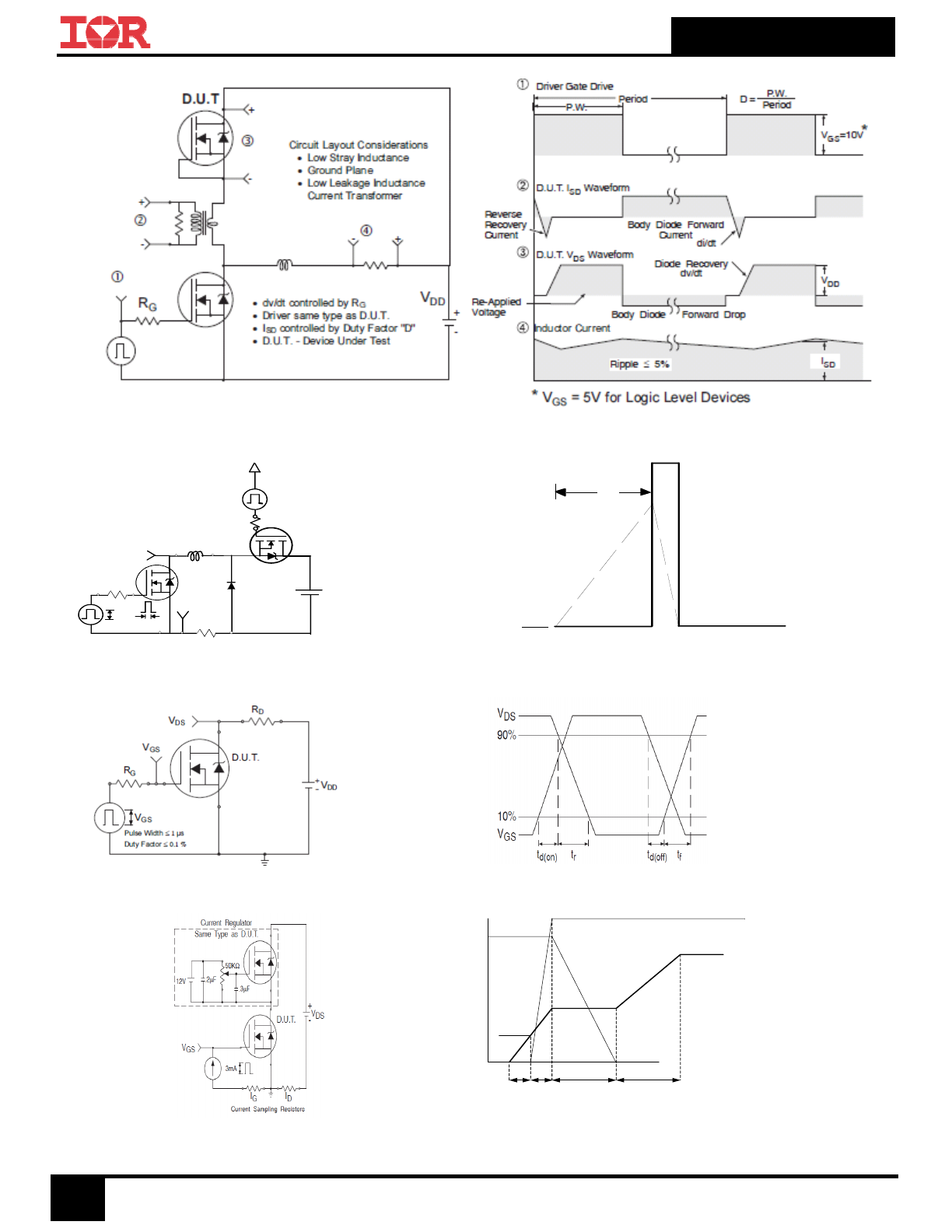
Fig 21. Peak Diode Recovery dv/dt Test Circuit for N-Channel HEXFET
®
Power MOSFETs
Fig 22a. Unclamped Inductive Test Circuit
R G
I
AS
0.01
tp
D.U.T
L
VDS
+
- VDD
DRIVER
A
15V
20V
Fig 23a. Switching Time Test Circuit
Fig 24a. Gate Charge Test Circuit
tp
V
(BR)DSS
I
AS
Fig 22b. Unclamped Inductive Waveforms
Fig 23b. Switching Time Waveforms
Vds
Vgs
Id
Vgs(th)
Qgs1 Qgs2
Qgd
Qgodr
Fig 24b. Gate Charge Waveform
IRFS4321-7PPbF
8
www.irf.com
© 2013 International Rectifier
June 14, 2013
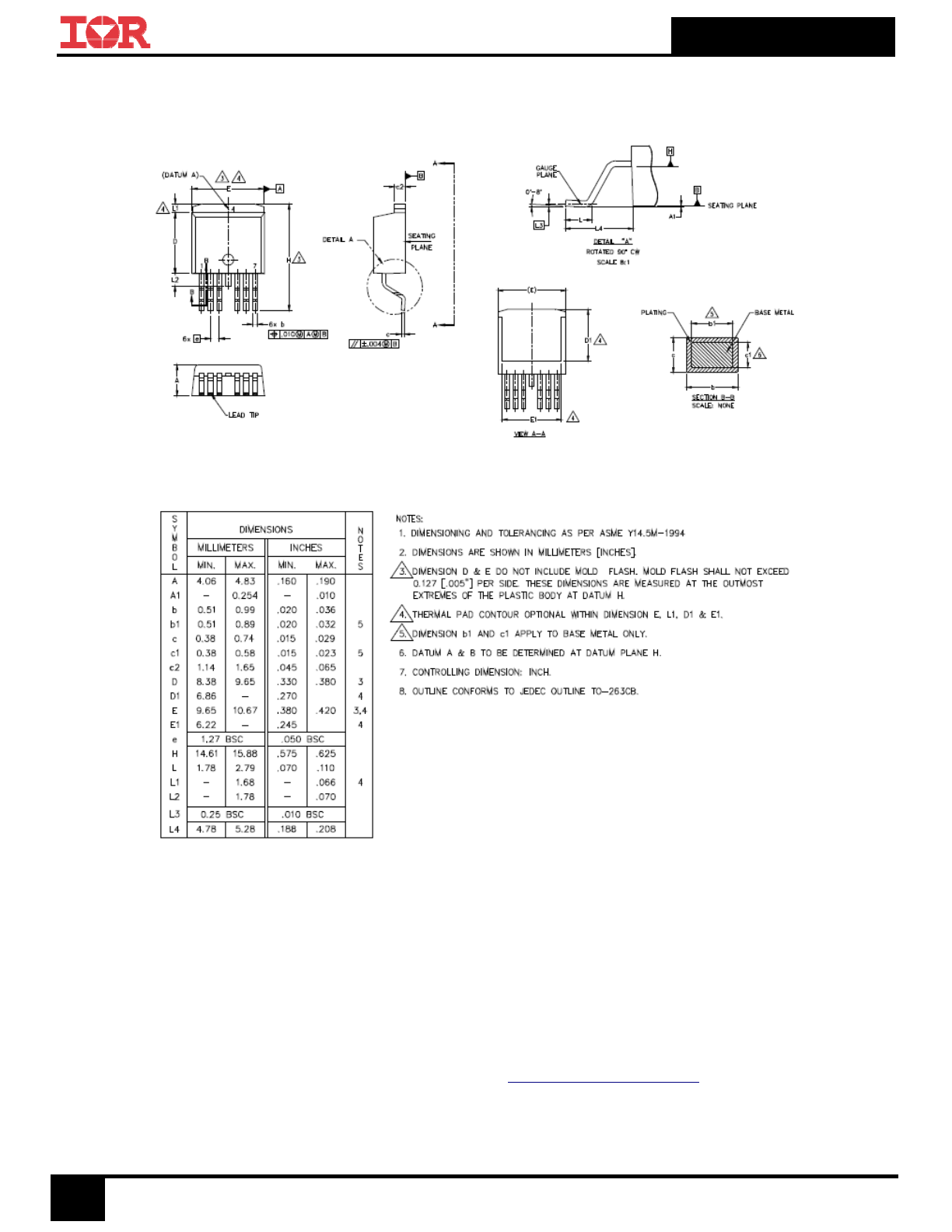
D
2
Pak-7Pin Package Outline (Dimensions are shown in millimeters (inches))
Note: For the most current drawing please refer to IR website at
http://www.irf.com/package/
IRFS4321-7PPbF
9
www.irf.com
© 2013 International Rectifier
June 14, 2013
D
2
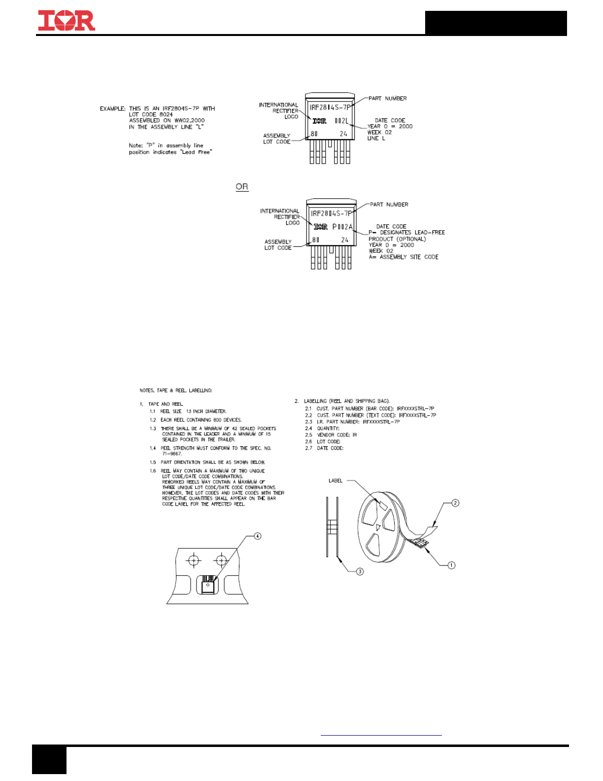
Pak-7Pin Part Marking Information
D2Pak-7Pin Tape and Reel
Note: For the most current drawing please refer to IR website at
http://www.irf.com/package/
IRFS4321-7PPbF
10
www.irf.com
© 2013 International Rectifier
June 14, 2013
† Qualification standards can be found at International Rectifier’s web site
: http://www.irf.com/product-info/reliability/
†† Applicable version of JEDEC standard at the time of product release.
IR WORLD HEADQUARTERS: 101 N. Sepulveda Blvd., El Segundo, California 90245, USA
To contact International Rectifier, please visit
http://www.irf.com/whoto-call/
Qualification Information
†
Qualification Level
Industrial
(per JEDEC JESD47F)
††
Moisture Sensitivity Level
D
2
Pak-7Pin MSL1
RoHS Compliant
Yes