
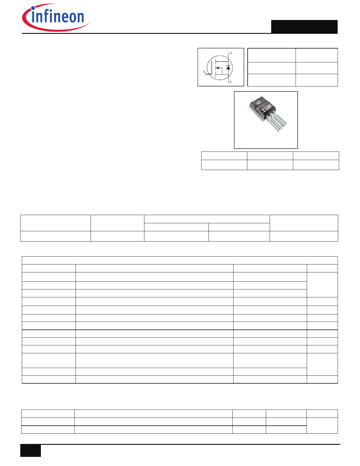
IRFIZ44NPbF
V
DSS
55V
R
DS(on)
0.024
I
D
31A
Description
Fifth Generation HEXFETs from International Rectifier utilize
advanced processing techniques to achieve extremely low on-
resistance per silicon area. This benefit, combined with the fast
switching speed and ruggedized device design that HEXFET
Power MOSFETs are well known for, provides the designer with
an extremely efficient and reliable device for use in a wide variety
of applications.
The TO-220 Full Pak eliminates the need for additional insulating
hardware in commercial-industrial applications. The molding
compound used provides a high isolation capability and a low
thermal resistance between the tab and external heat sink. This
isolation is equivalent to using a 100 micron mica barrier with
standard TO-220 product. The Fullpak is mounted to a heat sink
using a single clip or by a single screw fixing.
1
2017-04-27
Absolute Maximum Ratings
Symbol Parameter
Max.
Units
I
D
@ T
C
= 25°C
Continuous Drain Current, V
GS
@ 10V
31
A
I
D
@ T
C
= 100°C
Continuous Drain Current, V
GS
@ 10V
22
I
DM
Pulsed Drain Current 160
P
D
@T
C
= 25°C
Maximum Power Dissipation
45
W
Linear Derating Factor
0.3
W/°C
V
GS
Gate-to-Source Voltage
± 20
V
E
AS
Single Pulse Avalanche Energy (Thermally Limited) 210
mJ
I
AR
Avalanche Current 25
A
E
AR
Repetitive Avalanche Energy 4.5
mJ
dv/dt
Peak Diode Recovery dv/dt 5.0
V/ns
T
J
Operating Junction and
-55 to + 175
T
STG
Storage Temperature Range
°C
Soldering Temperature, for 10 seconds (1.6mm from case)
300
Mounting torque, 6-32 or M3 screw
10 lbf•in (1.1N•m)
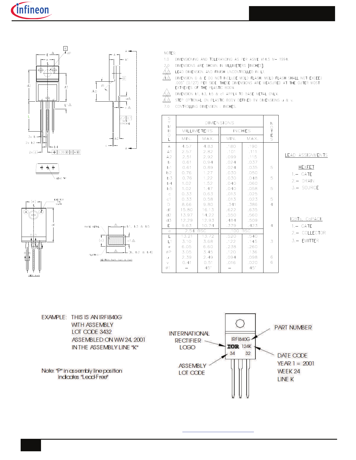
G D S
Gate Drain Source
Advanced Process Technology
Isolated
Package
High Voltage Isolation = 2.5KVRMS
Sink to Lead Creepage Dist. = 4.8mm
Fully Avalanche Rated
Lead-Free
HEXFET
®
Power MOSFET
TO-220 Full-Pak
Base Part Number
Package Type
Standard Pack
Orderable Part Number
Form Quantity
IRFIZ44NPbF
TO-220 Full-Pak
Tube
50 IRFIZ44NPbF
Thermal Resistance
Symbol Parameter
Typ.
Max.
Units
R
JC
Junction-to-Case
–––
3.3
R
JA
Junction-to-Ambient
–––
65
°C/W
G
D
S
IRFIZ44NPbF
2
2017-04-27
Notes:
Repetitive rating; pulse width limited by max. junction temperature. (See fig. 11)
starting T
J
= 25°C, L = 470
µ
H, R
G
= 25
, I
AS
= 25A (See fig. 12)
I
SD
25A, di/dt 320A/µs, V
DD
V
(BR)DSS
, T
J
175°C.
Pulse width
300µs; duty cycle 2%.
t=60s, ƒ=60Hz
Uses IRFZ44N data and test conditions.
Electrical Characteristics @ T
J
= 25°C (unless otherwise specified)
Parameter Min.
Typ.
Max.
Units
Conditions
V
(BR)DSS
Drain-to-Source Breakdown Voltage
55
–––
–––
V V
GS
= 0V, I
D
= 250µA
V
(BR)DSS
/
T
J
Breakdown Voltage Temp. Coefficient
––– 0.055 ––– V/°C Reference to 25°C, I
D
= 1mA
R
DS(on)
Static Drain-to-Source On-Resistance
–––
––– 0.024
V
GS
= 10V, I
D
= 17A
V
GS(th)
Gate Threshold Voltage
2.0
–––
4.0
V V
DS
= V
GS
, I
D
= 250µA
gfs
Forward Trans conductance
17
–––
–––
S V
DS
= 25V, I
D
= 25A
I
DSS
Drain-to-Source Leakage Current
––– ––– 25
µA
V
DS
= 55V, V
GS
= 0V
––– ––– 250
V
DS
= 55V,V
GS
= 0V,T
J
=150°C
I
GSS
Gate-to-Source Forward Leakage
–––
–––
100
nA
V
GS
= 20V
Gate-to-Source Reverse Leakage
–––
––– -100
V
GS
= -20V
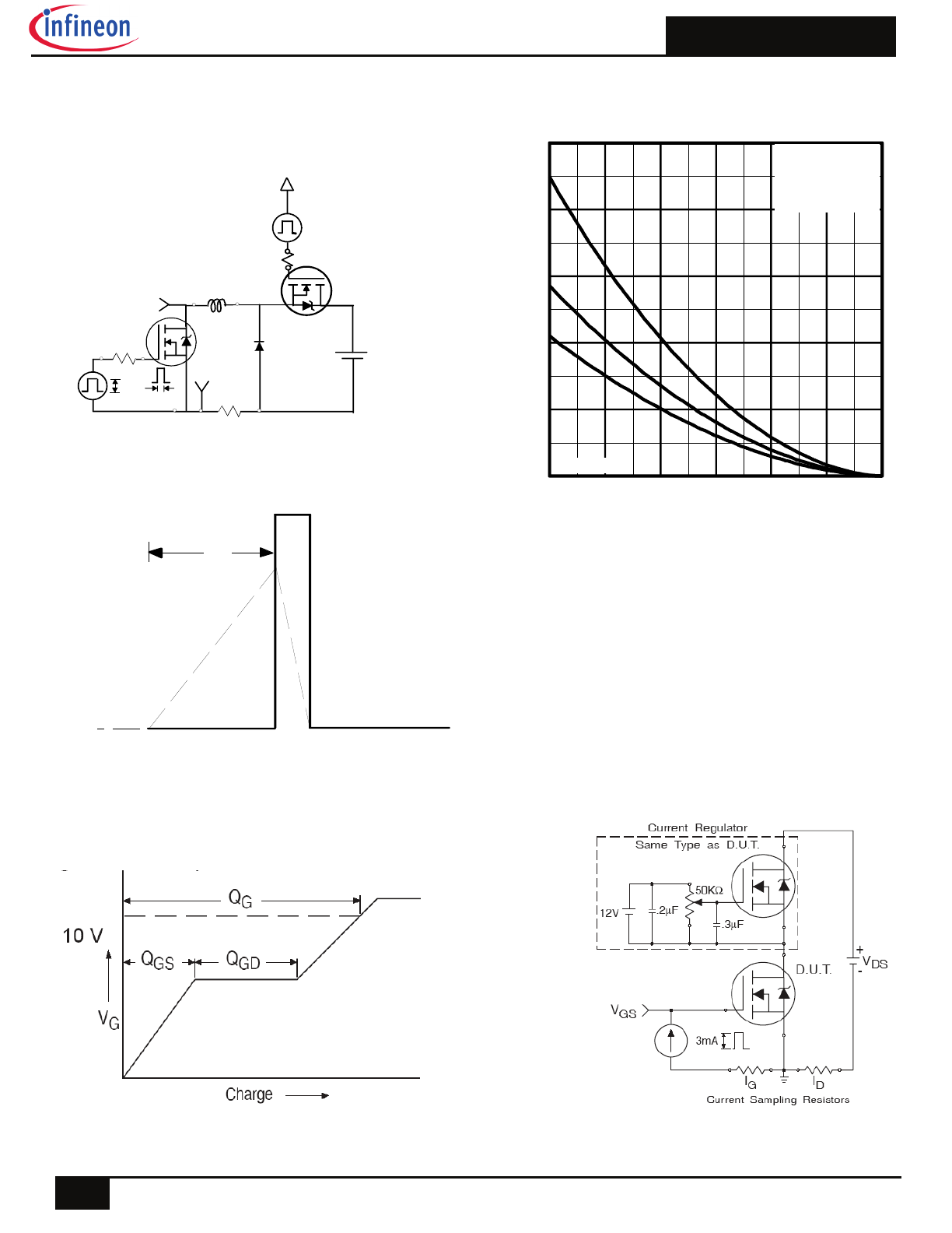
Q
g
Total Gate Charge
–––
–––
65
nC
I
D
= 25A
Q
gs
Gate-to-Source Charge
–––
–––
12
V
DS
= 44V
Q
gd
Gate-to-Drain Charge
–––
–––
27
V
GS
= 10V , See Fig. 6 and 13
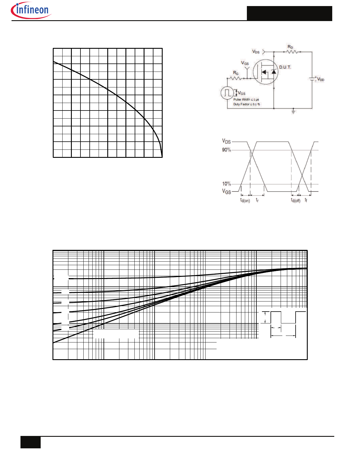
t
d(on)
Turn-On Delay Time
–––
7.3
–––
ns
V
DD
= 28V
t
r
Rise Time
–––
69
–––
I
D
=25A
t
d(off)
Turn-Off Delay Time
–––
47
–––
R
G
= 12
t
f
Fall Time
–––
60
–––
R
D
= 1.1
See Fig. 10
L
D
Internal Drain Inductance
–––
4.5
–––
nH
Between lead,
6mm (0.25in.)
L
S
Internal Source Inductance
–––
7.5
–––
from package
and center of die contact
C
iss
Input Capacitance
––– 1300 –––
V
GS
= 0V
C
oss
Output Capacitance
–––
410
–––
V
DS
= 25V
C
rss
Reverse Transfer Capacitance
–––
150
–––
ƒ = 1.0MHz, See Fig. 5
C
Drain to Sink Capacitance
–––
12
–––
ƒ = 1.0MHz
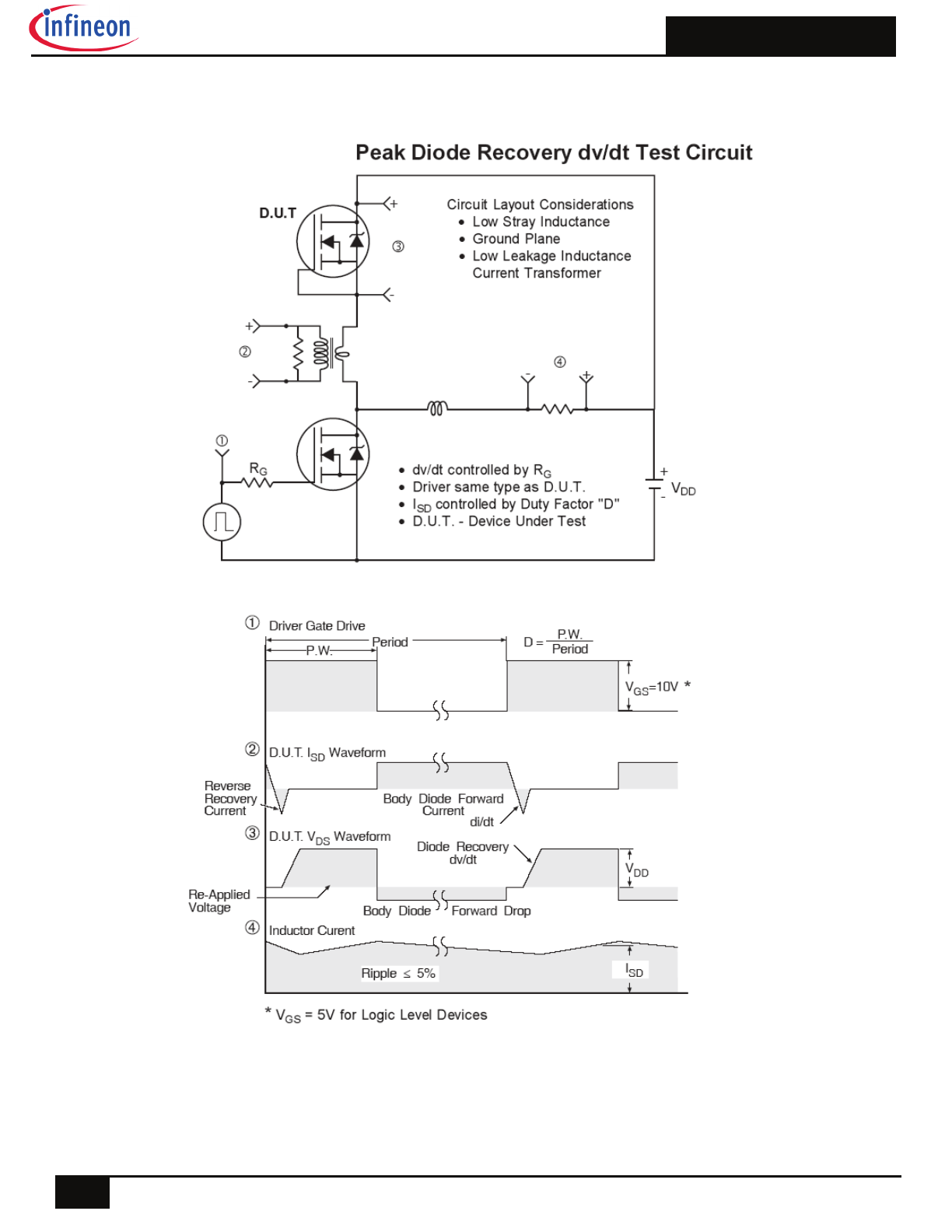
Source-Drain Ratings and Characteristics
Parameter
Min. Typ. Max. Units
Conditions
I
S
Continuous Source Current
––– ––– 31
A
MOSFET symbol
(Body Diode)
showing the
I
SM
Pulsed Source Current
––– ––– 160
integral reverse
(Body Diode)
p-n junction diode.
V
SD
Diode Forward Voltage
–––
–––
1.3
V T
J
= 25°C,I
S
= 17A,V
GS
= 0V
t
rr
Reverse Recovery Time
–––
65
98
ns T
J
= 25°C ,I
F
= 25A
Q
rr
Reverse Recovery Charge
–––
160
240
C di/dt = 100A/µs
t
on
Forward Turn-On Time
Intrinsic turn-on time is negligible (turn-on is dominated by L
S
+L
D
)
pF
IRFIZ44NPbF
3
2017-04-27
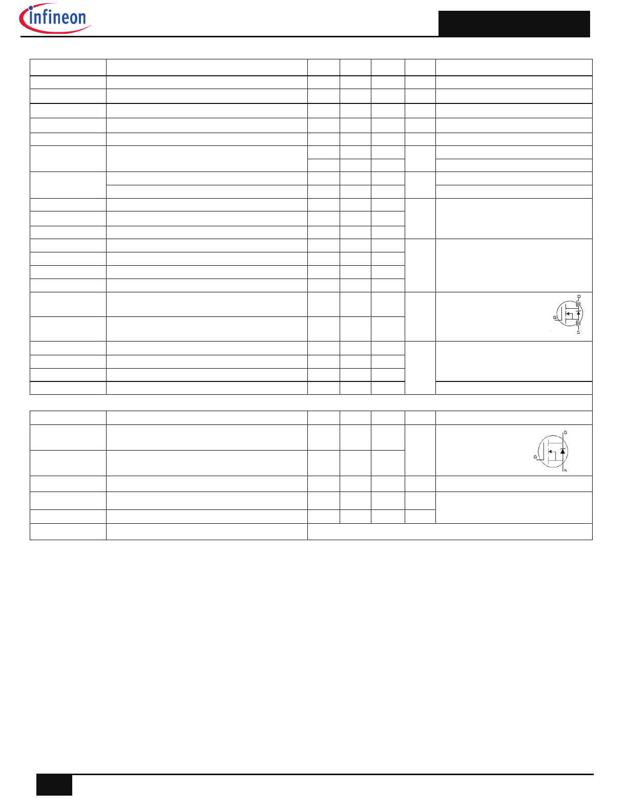
Fig. 2 Typical Output Characteristics
Fig. 3
Typical Transfer Characteristics
Fig. 4 Normalized On-Resistance
vs. Temperature
Fig. 1 Typical Output Characteristics
1
10
100
1000
0.1
1
10
100
I
, D
rai
n-
to-
S
our
ce Cur
rent
(
A
)
D
V , Drain-to-Source Voltage (V)
DS
VGS
TOP 15V
10V
8.0V
7.0V
6.0V
5.5V
5.0V
BOTTOM 4.5V
20µs PULSE WIDTH
T = 25°C
C
A
4.5V
1
10
100
1000
0.1
1
10
100
I
, D
rai
n-t
o-
S
ou
rc
e
C
urr
ent
(
A
)
D
V , Drain-to-Source Voltage (V)
DS
VGS
TOP 15V
10V
8.0V
7.0V
6.0V
5.5V
5.0V
BOTTOM 4.5V
A
4.5V
20µs PULSE WIDTH
T = 175°C
C
1
10
100
1000
4
5
6
7
8
9
10
T = 25°C
J
GS
V , Gate-to-Source Voltage (V)
D
I
, D
rai
n-
to
-So
u
rce
Curre
nt
(A)
A
V = 25V
20µs PULSE WIDTH
DS
T = 175°C
J
0.0
0.5
1.0
1.5
2.0
2.5
-60 -40 -20
0
20
40
60
80 100 120 140 160 180
J
T , Junction Temperature (°C)
R
,
Dra
in
-to
-S
ou
rc
e
O
n R
es
is
ta
nc
e
DS(
o
n)
(N
or
m
al
ized)
V = 10V
GS
A
I = 41A
D
IRFIZ44NPbF
4
2017-04-27
Fig 5. Typical Capacitance vs.
Drain-to-Source Voltage
Fig 8. Maximum Safe Operating Area
Fig. 7 Typical Source-to-Drain Diode
Forward Voltage
Fig 6. Typical Gate Charge vs.
Gate-to-Source Voltage
0
500
1000
1500
2000
2500
1
10
100
C,
Cap
ac
ita
nc
e
(p
F)
DS
V , Drain-to-Source Voltage (V)
A
V = 0V, f = 1MHz
C = C + C , C SHORTED
C = C
C = C + C
GS
iss gs gd ds
rss gd
oss ds gd
C
iss
C
oss
C
rss
0
4
8
12
16
20
0
10
20
30
40
50
60
70
Q , Total Gate Charge (nC)
G
V
, G
ate-
to-So
ur
ce
V
ol
tag
e (V
)
GS
A
FOR TEST CIRCUIT
SEE FIGURE 13
V = 44V
V = 28V
DS
DS
I = 25A
D
1
10
100
1000
0.5
1.0
1.5
2.0
2.5
3.0
T = 25°C
J
V = 0V
GS
V , Source-to-Drain Voltage (V)
I
, Reve
rs
e Dr
ain Cur
ren
t (
A
)
SD
SD
A
T = 175°C
J
1
10
100
1000
1
10
100
V , Drain-to-Source Voltage (V)
DS
I
, D
ra
in C
u
rr
ent
(
A
)
OPERATION IN THIS AREA LIMITED
BY R
D
DS(on)
10µs
100µs
1ms
10ms
A
T = 25°C
T = 175°C
Single Pulse
C
J
IRFIZ44NPbF
5
2017-04-27
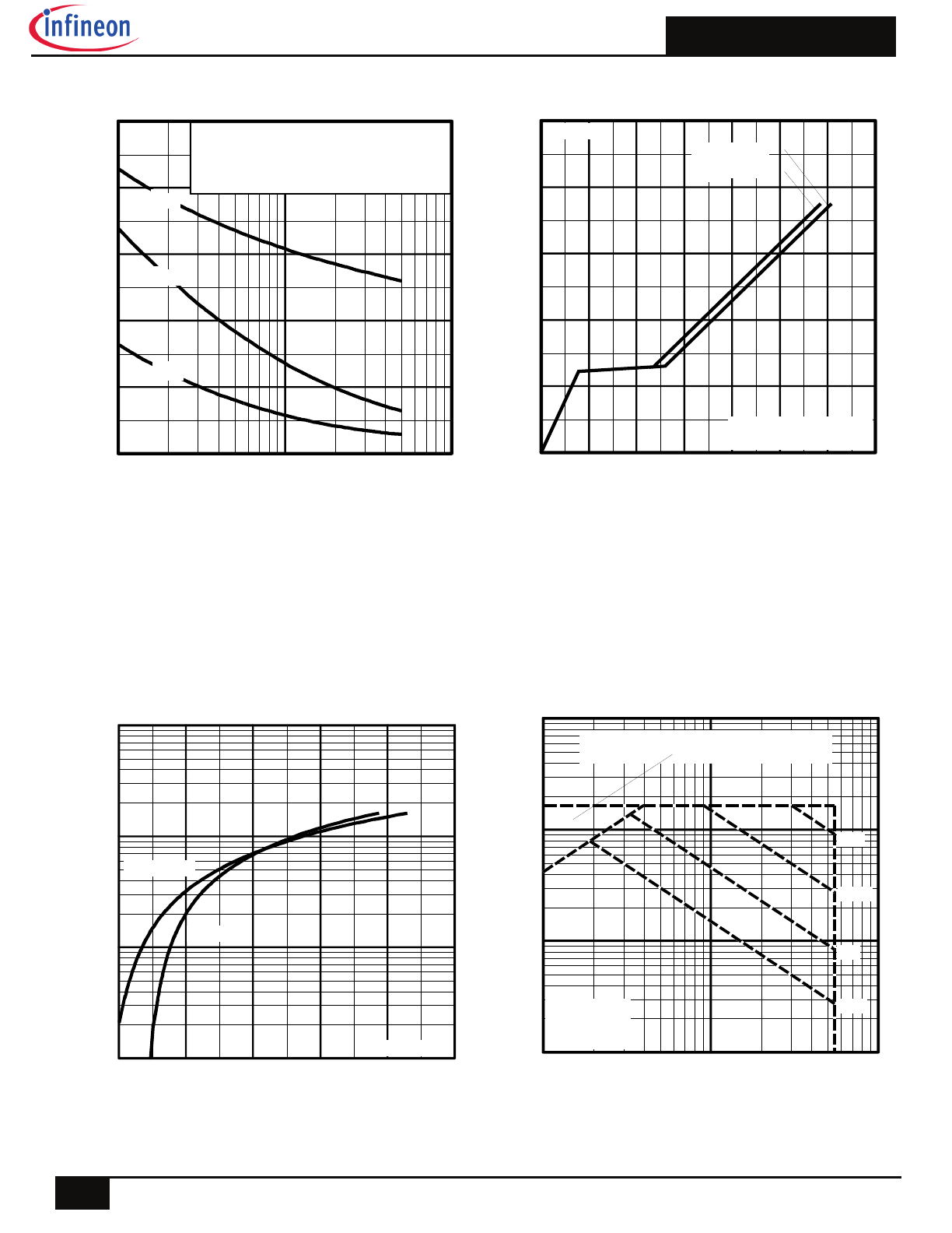
Fig 11. Maximum Effective Transient Thermal Impedance, Junction-to-Case
Fig 9. Maximum Drain Current vs. Case Temperature
Fig 10a. Switching Time Test Circuit
Fig 10b. Switching Time Waveforms
25
50
75
100
125
150
175
0
5
10
15
20
25
30
35
T , Case Temperature ( C)
I
, Drain
C
urren
t (A)
°
C
D
0.01
0.1
1
10
0.00001
0.0001
0.001
0.01
0.1
1
Notes:
1. Duty factor D =
t / t
2. Peak T = P
x Z
+ T
1
2
J
DM
thJC
C
P
t
t
DM
1
2
t , Rectangular Pulse Duration (sec)
Th
er
mal
R
e
sp
o
n
se
(Z
)
1
thJ
C
0.01
0.02
0.05
0.10
0.20
D = 0.50
SINGLE PULSE
(THERMAL RESPONSE)
IRFIZ44NPbF
6
2017-04-27
Fig 12c. Maximum Avalanche Energy
vs. Drain Current
Fig 12a. Unclamped Inductive Test Circuit
Fig 12b. Unclamped Inductive Waveforms
RG
IAS
0.01
tp
D.U.T
L
VDS
+
- VDD
DRIVER
A
15V
20V
tp
V
(BR)DSS
I
AS
Fig 13b. Gate Charge Test Circuit
Fig 13a. Gate Charge Waveform
0
100
200
300
400
500
25
50
75
100
125
150
175
J
E
, S
ing
le Pu
ls
e Av
al
an
ch
e E
ne
rg
y (mJ
)
AS
I
TOP 10A
18A
BOTTOM 25A
A
Starting T , Junction Temperature (°C)
V = 25V
D
DD
IRFIZ44NPbF
7
2017-04-27
Fig 14. Peak Diode Recovery dv/dt Test Circuit for N-Channel HEXFET® Power MOSFETs
IRFIZ44NPbF
8
2017-04-27
TO-220 Full-Pak Package Outline (Dimensions are shown in millimeters (inches))
TO-220 Full-Pak Part Marking Information
TO-220AB Full-Pak packages are not recommended for Surface Mount Application.
Note: For the most current drawing please refer to website at
http://www.irf.com/package/
IRFIZ44NPbF
9
2017-04-27
Qualification Information
Qualification Level
Industrial
(per JEDEC JESD47F)
†
TO-220 Full-Pak
N/A
RoHS Compliant
Yes
Moisture Sensitivity Level
† Applicable version of JEDEC standard at the time of product release.
Trademarks of Infineon Technologies AG
µHVIC™, µIPM™, µPFC™, AU-ConvertIR™, AURIX™, C166™, CanPAK™, CIPOS™, CIPURSE™, CoolDP™, CoolGaN™, COOLiR™, CoolMOS™, CoolSET™,
CoolSiC™, DAVE™, DI-POL™, DirectFET™, DrBlade™, EasyPIM™, EconoBRIDGE™, EconoDUAL™, EconoPACK™, EconoPIM™, EiceDRIVER™, eupec™, FCOS™,
GaNpowIR™, HEXFET™, HITFET™, HybridPACK™, iMOTION™, IRAM™, ISOFACE™, IsoPACK™, LEDrivIR™, LITIX™, MIPAQ™, ModSTACK™, my-d™, NovalithIC™,
OPTIGA™, OptiMOS™, ORIGA™, PowIRaudio™, PowIRStage™, PrimePACK™, PrimeSTACK™, PROFET™, PRO-SIL™, RASIC™, REAL3™, SmartLEWIS™, SOLID
FLASH™, SPOC™, StrongIRFET™, SupIRBuck™, TEMPFET™, TRENCHSTOP™, TriCore™, UHVIC™, XHP™, XMC™
Trademarks updated November 2015
Other Trademarks
All referenced product or service names and trademarks are the property of their respective owners.
Edition 2016-04-19
Published by
Infineon Technologies AG
81726 Munich, Germany
© 2016 Infineon Technologies AG.
All Rights Reserved.
Do you have a question about this
document?
Email:
erratum@infineon.com
Document reference
ifx1
IMPORTANT NOTICE
The information given in this document shall in no
event be regarded as a guarantee of conditions or
characteristics (“Beschaffenheitsgarantie”) .
With respect to any examples, hints or any typical
values stated herein and/or any information
regarding the application of the product, Infineon
Technologies hereby disclaims any and all
warranties and liabilities of any kind, including
without limitation warranties of non-infringement
of intellectual property rights of any third party.
In addition, any information given in this
document is subject to customer’s compliance
with its obligations stated in this document and
any applicable legal requirements, norms and
standards concerning customer’s products and
any use of the product of Infineon Technologies in
customer’s applications.
The data contained in this document is exclusively
intended for technically trained staff. It is the
responsibility of customer’s technical
departments to evaluate the suitability of the
product for the intended application and the
completeness of the product information given in
this document with respect to such application.
For further information on the product, technology,
delivery terms and conditions and prices please
contact your nearest Infineon Technologies office
(
www.infineon.com
).
Please note that this product is not qualified
according to the AEC Q100 or AEC Q101 documents
of the Automotive Electronics Council.
WARNINGS
Due to technical requirements products may
contain dangerous substances. For information on
the types in question please contact your nearest
Infineon Technologies office.
Except as otherwise explicitly approved by Infineon
Technologies in a written document signed by
authorized representatives of Infineon
Technologies, Infineon Technologies’ products
may not be used in any applications where a
failure of the product or any consequences of the
use thereof can reasonably be expected to result in
personal injury.
Revision History
Date Comments
04/27/2017
Changed datasheet with Infineon logo - all pages.
Corrected Package Outline on page 8.
Added disclaimer on last page.