
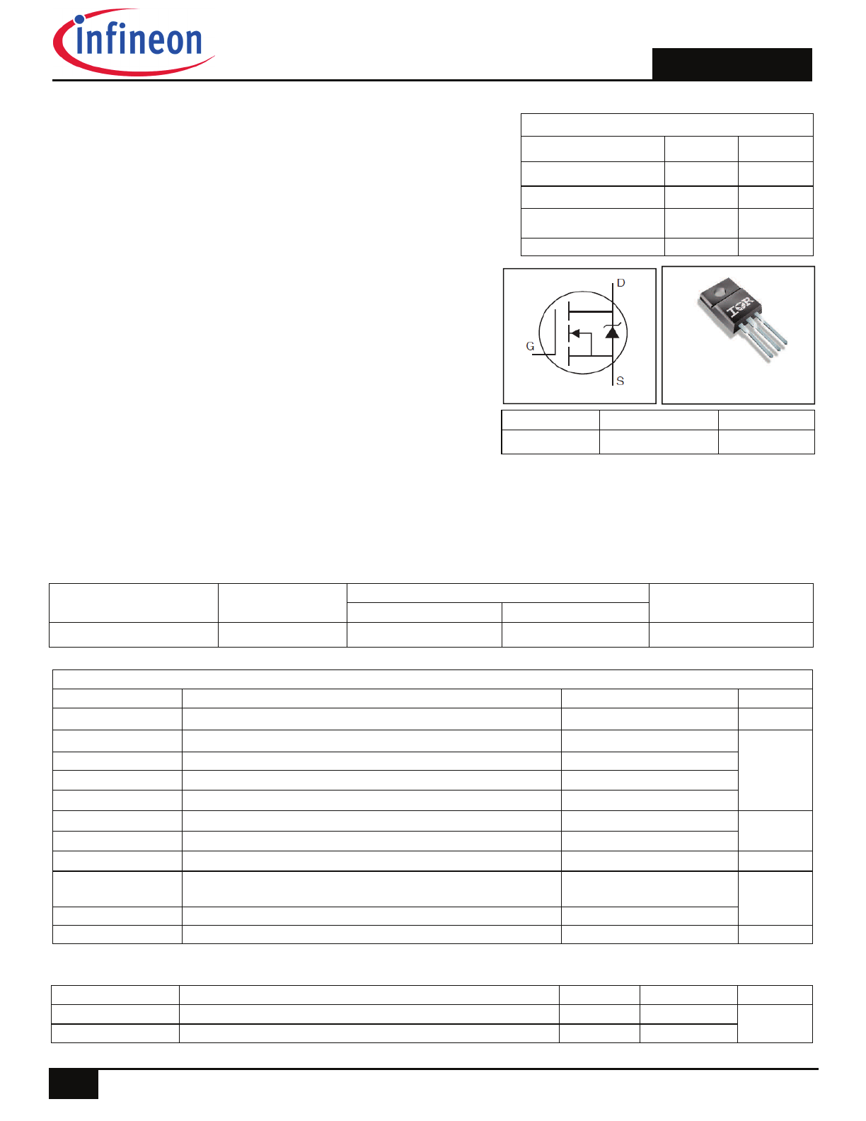
IRFI4229PbF
Description
This HEXFET
®
Power MOSFET is specifically designed for Sustain; Energy Recovery & Pass switch applications in
Plasma Display Panels. This MOSFET utilizes the latest processing techniques to achieve low on-resistance per silicon
area and low E
PULSE
rating. Additional features of this MOSFET are 150°C operating junction temperature and high
repetitive peak current capability. These features combine to make this MOSFET a highly efficient, robust and reliable
device for PDP driving applications
1
2017-04-27
Absolute Maximum Ratings
Symbol Parameter
Max.
Units
V
GS
Gate-to-Source Voltage
± 30
V
I
D
@ T
C
= 25°C
Continuous Drain Current, V
GS
@ 10V
19
A
I
D
@ T
C
= 100°C
Continuous Drain Current, V
GS
@ 10V
12
I
DM
Pulsed Drain Current 72
I
RP
@ T
C
= 100°C
Repetitive Peak Current 32
P
D
@T
C
= 25°C
Maximum Power Dissipation
46
W
P
D
@T
C
= 100°C
Maximum Power Dissipation
18
Linear Derating Factor
0.37
W/°C
T
J
Operating Junction and
T
STG
Storage Temperature Range
°C
Soldering Temperature, for 10 seconds (1.6mm from case)
300
Mounting torque, 6-32 or M3 screw
10 lbf•in (1.1N•m)
-40 to + 150
G D S
Gate Drain
Source
Features
Advanced Process Technology
Key Parameters Optimized for PDP Sustain,
Energy Recovery and Pass Switch Applications
Low
E
PULSE
Rating to Reduce Power
Dissipation in PDP Sustain, Energy Recovery
and Pass Switch Applications
Low
Q
G
for Fast Response
High Repetitive Peak Current Capability for
Reliable
Operation
Short Fall & Rise Times for Fast Switching
150°C Operating Junction Temperature for
Improved
Ruggedness
Repetitive Avalanche Capability for Robustness and
Reliability
HEXFET
®
Power MOSFET
TO-220 Full-Pak
Base Part Number
Package Type
Standard Pack
Orderable Part Number
Form Quantity
IRFI4229PbF
TO-220 Full-Pak
Tube
50 IRFI4229PbF
Thermal Resistance
Symbol Parameter
Typ.
Max.
Units
R
JC
Junction-to-Case –––
2.73
R
JA
Junction-to-Ambient
–––
65
°C/W
G
D
S
Key Parameters
V
DS
max 250
V
V
DS (Avalanche)
typ. 300
V
R
DS(ON)
typ. @ 10V
38
m
I
RP
max @ T
C
= 100°C
32
A
T
J
max
150
°C
IRFI4229PbF
2
2017-04-27
Notes:
Repetitive rating; pulse width limited by max. junction temperature.
starting T
J
= 25°C, L = 1.9mH, R
G
= 25
, I
AS
= 11A.
Pulse width
400µs; duty cycle 2%.
R
θ
is measured at T
J
of approximately 90°C.
Half sine wave with duty cycle = 0.25, ton=1μsec.
Electrical Characteristics @ T
J
= 25°C (unless otherwise specified)
Parameter Min.
Typ.
Max.
Units
Conditions
V
(BR)DSS
Drain-to-Source Breakdown Voltage
250
–––
–––
V
V
GS
= 0V, I
D
= 250µA
V
(BR)DSS
/
T
J
Breakdown Voltage Temp. Coefficient
–––
340
––– mV/°C Reference to 25°C, I
D
= 1mA
R
DS(on)
Static Drain-to-Source On-Resistance
–––
38
46
m
V
GS
= 10V, I
D
= 11A
V
GS(th)
Gate Threshold Voltage
3.0
–––
5.0
V
V
DS
= V
GS
, I
D
= 250µA
V
GS(th)/
T
J
Gate Threshold Voltage Temp. Coefficient –––
-12
––– mV/°C
I
DSS
Drain-to-Source Leakage Current
––– ––– 20
V
DS
= 250V, V
GS
= 0V
––– ––– 200
V
DS
= 250V,V
GS
= 0V,T
J
=150°C
I
GSS
Gate-to-Source Forward Leakage
–––
–––
100
nA
V
GS
= 20V
Gate-to-Source Reverse Leakage
–––
––– -100
V
GS
= -20V
gfs
Forward Trans conductance
26
–––
–––
S
V
DS
= 25V, I
D
= 11A
Q
g
Total Gate Charge
–––
73
110
nC
I
D
= 11A,V
DS
= 125V
Q
gd
Gate-to-Drain Charge
–––
24
–––
V
GS
= 10V
t
d(on)
Turn-On Delay Time
–––
18
–––
ns
V
DD
= 125V, V
GS
= 10V
t
r
Rise Time
–––
17
–––
I
D
= 11A
t
d(off)
Turn-Off Delay Time
–––
32
–––
R
G
= 2.4
t
f
Fall Time
–––
13
–––
See Fig. 22
t
st
Shoot Through Blocking Time
100
–––
–––
ns V
DD
= 200V,V
GS
= 15V,R
G
= 5.1
E
PULSE
Energy per Pulse
––– 770 –––
µJ
L = 220nH, C = 0.3µF, V
GS
= 15V
V
DD
= 200V, R
G
= 5.1
T
J
= 25°C
––– 1380 –––
L = 220nH, C = 0.3µF, V
GS
= 15V
V
DD
= 200V, R
G
= 5.1
T
J
= 100°C
C
iss
Input Capacitance
––– 4480 –––
pF
V
GS
= 0V
C
oss
Output Capacitance
–––
400
–––
V
DS
= 25V
C
rss
Reverse Transfer Capacitance
–––
100
–––
ƒ = 1.0MHz
C
oss
eff.
Effective Output Capacitance
–––
270
–––
V
GS
= 0V, V
DS
= 0V to 200V
L
D
Internal Drain Inductance
–––
4.5
–––
nH
Between lead,
6mm (0.25in.)
L
S
Internal Source Inductance
–––
7.5
–––
from package
and center of die contact
µA
Diode Characteristics
Parameter
Min. Typ. Max. Units
Conditions
I
S
@ T
C
= 25°C
Continuous Source Current
––– ––– 18
A
MOSFET symbol
(Body Diode)
showing the
I
SM
Pulsed Source Current
––– ––– 72
integral reverse
(Body Diode)
p-n junction diode.
V
SD
Diode Forward Voltage
–––
–––
1.3
V T
J
= 25°C,I
S
= 11A,V
GS
= 0V
t
rr
Reverse Recovery Time
–––
120
180
ns T
J
= 25°C ,I
F
= 11A, V
DD
= 50V
Q
rr
Reverse Recovery Charge
–––
540
810
nC di/dt = 100A/µs
Avalanche Characteristics
Parameter
Typ. Max. Units
E
AS
Single Pulse Avalanche Energy
––– 110
E
AR
Repetitive Avalanche Energy
––– 4.6
V
DS(Avalanche)
Repetitive Avalanche Voltage
300 ––– V
I
AS
Avalanche Current
––– 11 A
mJ
IRFI4229PbF
3
2017-04-27
Fig. 2. Typical Output Characteristics
Fig. 3.
Typical Transfer Characteristics
Fig. 1. Typical Output Characteristics
Fig 6. Typical E
PULSE
vs. Drain Current
Fig 5. Typical E
PULSE
vs. Drain-to-Source Voltage
0.1
1
10
100
VDS, Drain-to-Source Voltage (V)
0.01
0.1
1
10
100
1000
I D
, D
ra
in
-t
o
-S
ou
rc
e
C
u
rr
en
t
(A
)
VGS
TOP 15V
10V
8.0V
7.0V
6.5V
6.0V
5.5V
BOTTOM
5.0V
60µs PULSE WIDTH
Tj = 25°C
5.0V
0.1
1
10
100
VDS, Drain-to-Source Voltage (V)
0.1
1
10
100
1000
I D
, D
ra
in
-t
o-
S
ou
rc
e
C
u
rr
en
t (
A
)
5.0V
60µs PULSE WIDTH
Tj = 150°C
VGS
TOP 15V
10V
8.0V
7.0V
6.5V
6.0V
5.5V
BOTTOM
5.0V
3
4
5
6
7
VGS, Gate-to-Source Voltage (V)
0.1
1
10
100
I D
, D
ra
in
-t
o-
S
ou
rc
e
C
ur
re
nt
(A
)
TJ = 25°C
TJ = 150°C
VDS = 25V
60µs PULSE WIDTH
-60 -40 -20 0 20 40 60 80 100 120 140 160
TJ , Junction Temperature (°C)
0.0
0.5
1.0
1.5
2.0
2.5
3.0
R
D
S
(o
n)
,
D
ra
in
-t
o-
S
ou
rc
e
O
n
R
es
is
ta
nc
e
(
N
or
m
al
iz
ed
)
ID = 11A
VGS = 10V
140
150
160
170
180
190
200
210
VDS, Drain-to-Source Voltage (V)
200
400
600
800
1000
1200
1400
E
ne
rg
y
pe
r
P
ul
se
(
µJ
)
L = 220nH
C = 0.3µF
100°C
25°C
100
110
120
130
140
150
160
170
ID, Peak Drain Current (A)
0
200
400
600
800
1000
1200
1400
E
ne
rg
y
pe
r
P
ul
se
(
µJ
)
L = 220nH
C = variable
100°C
25°C
Fig. 4.
Normalized On-Resistance vs. Temperature
IRFI4229PbF
4
2017-04-27
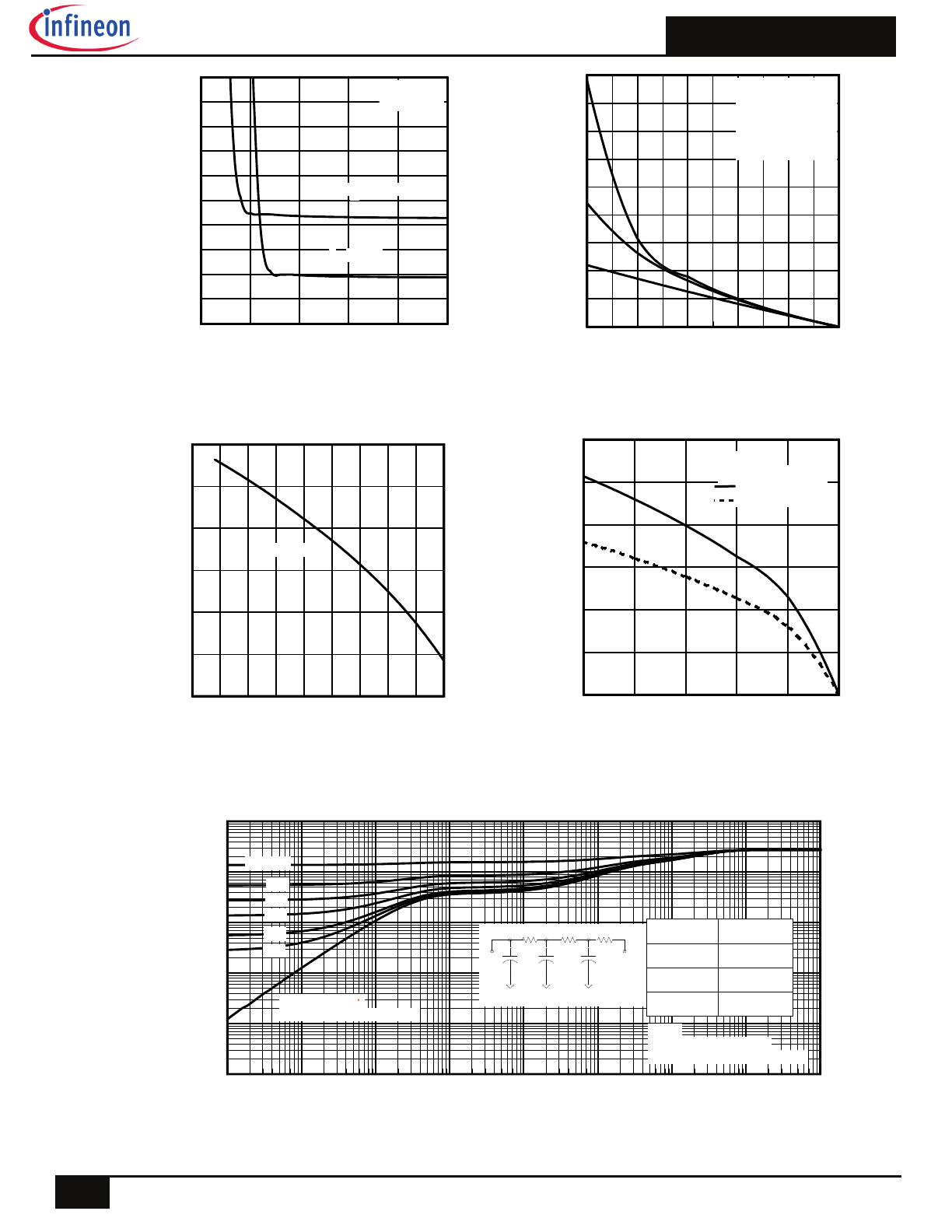
Fig 12. Maximum Safe Operating Area
Fig. 7. Typical E
PULSE
vs. Temperature
Fig 11. Maximum Drain Current vs. Case Temperature
20
40
60
80
100
120
140
160
Temperature (°C)
0
200
400
600
800
1000
1200
1400
1600
1800
E
ne
rg
y
pe
r
P
ul
se
(
µJ
)
L = 220nH
C = 0.3µF
C = 0.2µF
C = 0.1µF
0.2
0.4
0.6
0.8
1.0
VSD, Source-to-Drain Voltage (V)
0.1
1
10
100
I S
D
, R
ev
er
se
D
ra
in
C
ur
re
nt
(
A
)
TJ = 25°C
TJ = 150°C
VGS = 0V
1
10
100
1000
VDS, Drain-to-Source Voltage (V)
0
1000
2000
3000
4000
5000
6000
7000
C
, C
ap
ac
ita
nc
e
(p
F
)
VGS = 0V, f = 1 MHZ
Ciss = Cgs + Cgd, C ds SHORTED
Crss = Cgd
Coss = Cds + Cgd
Coss
Crss
Ciss
0
10
20
30
40
50
60
70
80
QG, Total Gate Charge (nC)
0.0
2.0
4.0
6.0
8.0
10.0
12.0
V
G
S
, G
at
e-
to
-S
ou
rc
e
V
ol
ta
ge
(
V
)
VDS= 200V
VDS= 125V
VDS= 50V
ID= 11A
Fig 8. Typical Source-Drain Diode Forward Voltage
25
50
75
100
125
150
TC , Case Temperature (°C)
0
2
4
6
8
10
12
14
16
18
20
I D
,
D
ra
in
C
ur
re
nt
(
A
)
Fig 9. Typical Capacitance vs.Drain-to-Source Voltage
1
10
100
1000
VDS, Drain-to-Source Voltage (V)
0.01
0.1
1
10
100
1000
I D
,
D
ra
in
-t
o-
S
ou
rc
e
C
ur
re
nt
(
A
)
OPERATION IN THIS AREA
LIMITED BY R DS(on)
Tc = 25°C
Tj = 150°C
Single Pulse
100µsec
1msec
10msec
Fig 10. Typical Gate Charge vs. Gate-to-Source Voltage
IRFI4229PbF
5
2017-04-27
Fig. 14. Maximum Avalanche Energy Vs. Temperature
Fig. 15. Threshold Voltage vs. Temperature
5
6
7
8
9
10
VGS, Gate -to -Source Voltage (V)
0
20
40
60
80
100
120
140
160
180
200
R
D
S
(o
n)
,
D
ra
in
-t
o
-S
o
ur
ce
O
n
R
es
is
ta
nc
e
(m
)
ID = 11A
TJ = 25°C
TJ = 125°C
25
50
75
100
125
150
Starting TJ , Junction Temperature (°C)
0
50
100
150
200
250
300
350
400
450
E
A
S
,
S
in
gl
e
P
ul
se
A
va
la
nc
he
E
ne
rg
y
(m
J)
ID
TOP 2.3A
2.7A
BOTTOM 11A
-75 -50 -25
0
25
50
75 100 125 150
TJ , Temperature ( °C )
2.0
3.0
4.0
5.0
V
G
S
(t
h)
, G
at
e
T
hr
es
ho
ld
V
ol
ta
ge
(
V
)
ID = 250µA
Fig. 13. On-Resistance Vs. Gate Voltage
25
50
75
100
125
150
Case Temperature (°C)
0
10
20
30
40
50
60
R
ep
et
iti
ve
P
ea
k
C
ur
re
nt
(
A
)
ton= 1µs
Duty cycle = 0.25
Half Sine Wave
Square Pulse
1E-006
1E-005
0.0001
0.001
0.01
0.1
1
10
100
t1 , Rectangular Pulse Duration (sec)
0.0001
0.001
0.01
0.1
1
10
T
he
rm
al
R
es
po
ns
e
(
Z
th
JC
)
0.20
0.10
D = 0.50
0.02
0.01
0.05
SINGLE PULSE
( THERMAL RESPONSE )
Notes:
1. Duty Factor D = t1/t2
2. Peak Tj = P dm x Zthjc + Tc
J
J
1
1
2
2
3
3
R
1
R
1
R
2
R
2
R
3
R
3
C
C
Ci=
iRi
Ci=
iRi
Ri (°C/W)
i (sec)
1.0580
0.162897
1.3076
2.426
0.3671
0.000287
Fig. 16. Typical Repetitive peak Current vs.
Case temperature
Fig 17. Maximum Effective Transient Thermal Impedance, Junction-to-Case
IRFI4229PbF
6
2017-04-27
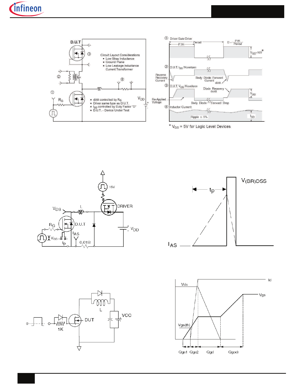
Fig 19a. Unclamped Inductive Test Circuit
Fig 19b. Unclamped Inductive Waveforms
Fig 20a. Gate Charge Test Circuit
Fig 20b. Gate Charge Waveform
Fig 18. Diode Reverse Recovery Test Circuit for N-Channel HEXFET® Power MOSFETs
IRFI4229PbF
7
2017-04-27
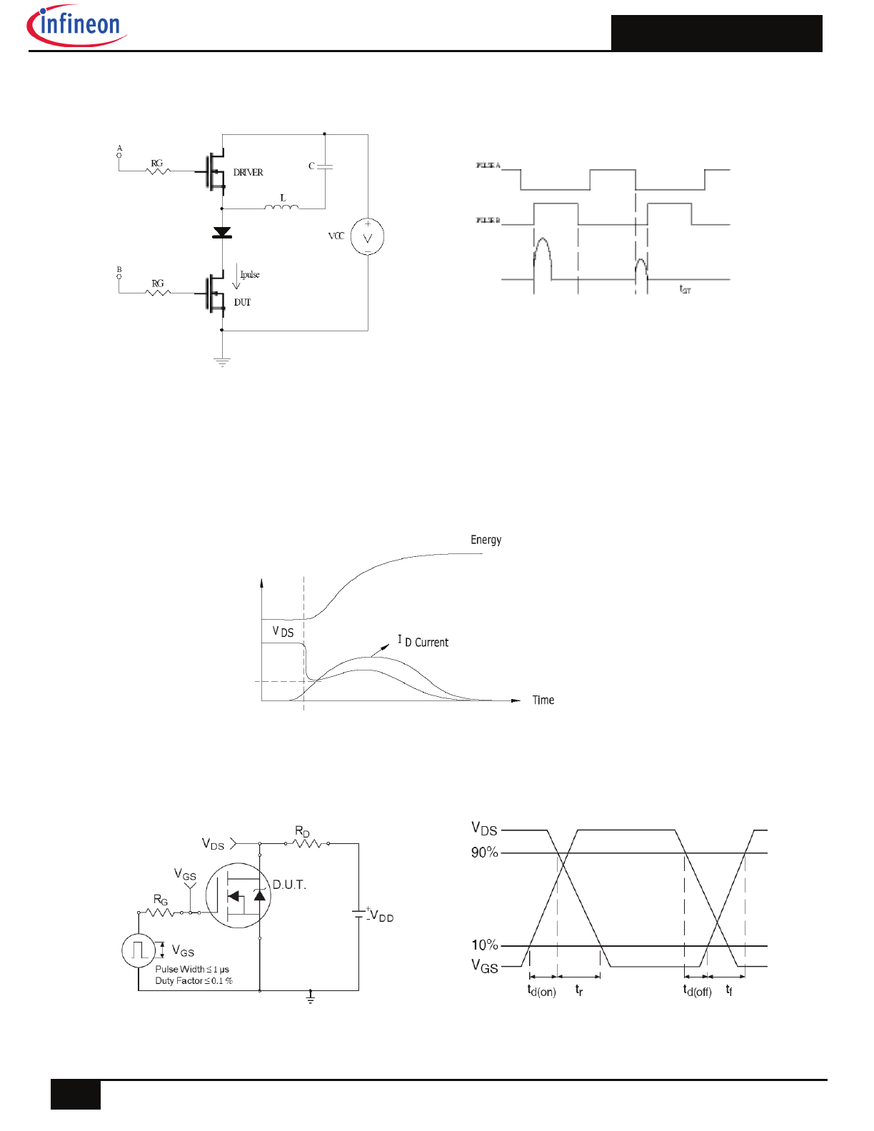
Fig 21a. t
st
and E
PULSE
Test Circuit
Fig 21b. t
st
Test Waveforms
Fig 22a. Switching Time Test Circuit
Fig 22b. Switching Time Waveforms
Fig 21c. E
PULSE
Test Waveforms
IRFI4229PbF
8
2017-04-27
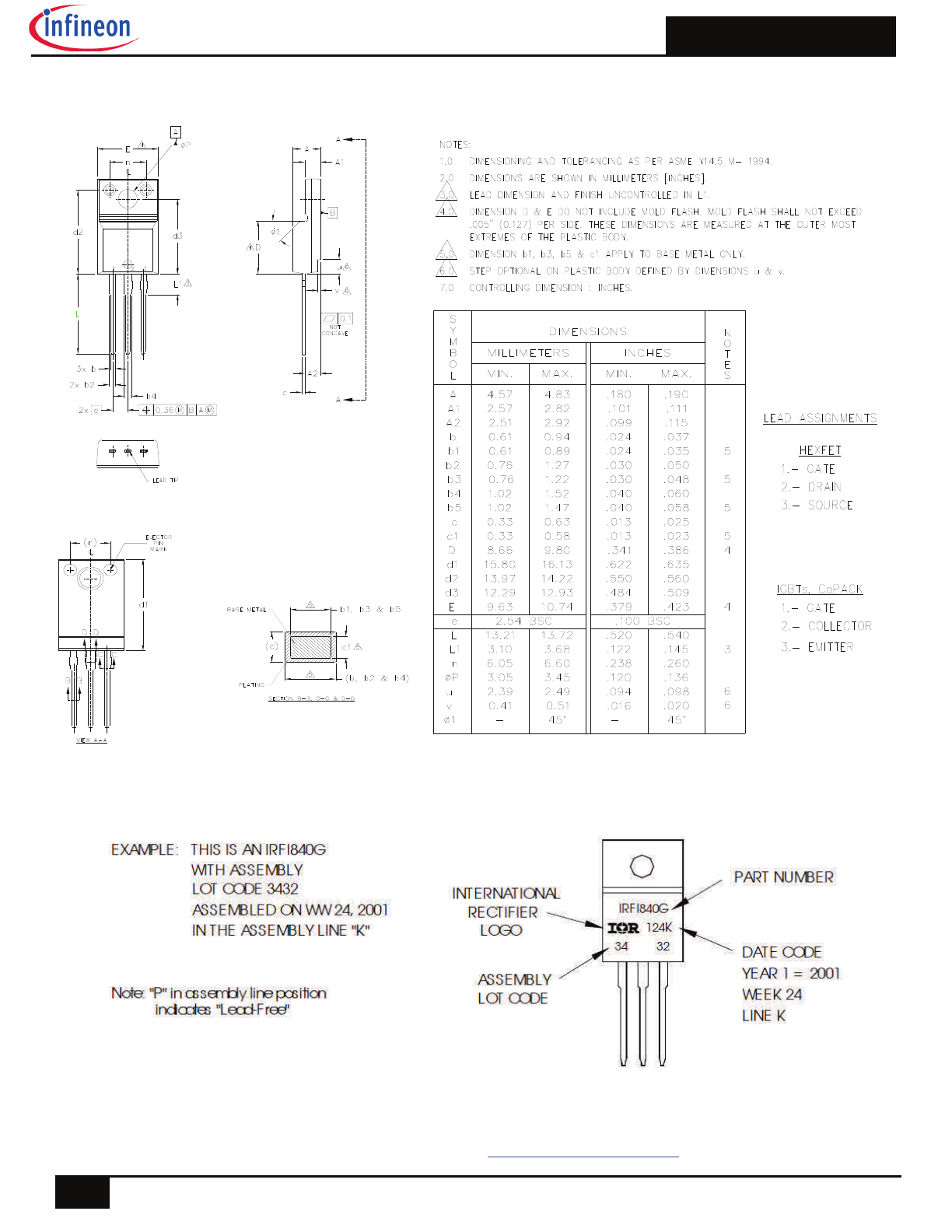
TO-220 Full-Pak Package Outline (Dimensions are shown in millimeters (inches))
TO-220 Full-Pak Part Marking Information
TO-220AB Full-Pak packages are not recommended for Surface Mount Application.
Note: For the most current drawing please refer to website at
http://www.irf.com/package/
IRFI4229PbF
9
2017-04-27
Qualification Information
Qualification Level
Industrial
(per JEDEC JESD47F)
†
TO-220 Full-Pak
N/A
RoHS Compliant
Yes
Moisture Sensitivity Level
† Applicable version of JEDEC standard at the time of product release.
Trademarks of Infineon Technologies AG
µHVIC™, µIPM™, µPFC™, AU-ConvertIR™, AURIX™, C166™, CanPAK™, CIPOS™, CIPURSE™, CoolDP™, CoolGaN™, COOLiR™, CoolMOS™, CoolSET™,
CoolSiC™, DAVE™, DI-POL™, DirectFET™, DrBlade™, EasyPIM™, EconoBRIDGE™, EconoDUAL™, EconoPACK™, EconoPIM™, EiceDRIVER™, eupec™, FCOS™,
GaNpowIR™, HEXFET™, HITFET™, HybridPACK™, iMOTION™, IRAM™, ISOFACE™, IsoPACK™, LEDrivIR™, LITIX™, MIPAQ™, ModSTACK™, my-d™, NovalithIC™,
OPTIGA™, OptiMOS™, ORIGA™, PowIRaudio™, PowIRStage™, PrimePACK™, PrimeSTACK™, PROFET™, PRO-SIL™, RASIC™, REAL3™, SmartLEWIS™, SOLID
FLASH™, SPOC™, StrongIRFET™, SupIRBuck™, TEMPFET™, TRENCHSTOP™, TriCore™, UHVIC™, XHP™, XMC™
Trademarks updated November 2015
Other Trademarks
All referenced product or service names and trademarks are the property of their respective owners.
Edition 2016-04-19
Published by
Infineon Technologies AG
81726 Munich, Germany
© 2016 Infineon Technologies AG.
All Rights Reserved.
Do you have a question about this
document?
Email:
erratum@infineon.com
Document reference
ifx1
IMPORTANT NOTICE
The information given in this document shall in no
event be regarded as a guarantee of conditions or
characteristics (“Beschaffenheitsgarantie”) .
With respect to any examples, hints or any typical
values stated herein and/or any information
regarding the application of the product, Infineon
Technologies hereby disclaims any and all
warranties and liabilities of any kind, including
without limitation warranties of non-infringement
of intellectual property rights of any third party.
In addition, any information given in this
document is subject to customer’s compliance
with its obligations stated in this document and
any applicable legal requirements, norms and
standards concerning customer’s products and
any use of the product of Infineon Technologies in
customer’s applications.
The data contained in this document is exclusively
intended for technically trained staff. It is the
responsibility of customer’s technical
departments to evaluate the suitability of the
product for the intended application and the
completeness of the product information given in
this document with respect to such application.
For further information on the product, technology,
delivery terms and conditions and prices please
contact your nearest Infineon Technologies office
(
www.infineon.com
).
Please note that this product is not qualified
according to the AEC Q100 or AEC Q101 documents
of the Automotive Electronics Council.
WARNINGS
Due to technical requirements products may
contain dangerous substances. For information on
the types in question please contact your nearest
Infineon Technologies office.
Except as otherwise explicitly approved by Infineon
Technologies in a written document signed by
authorized representatives of Infineon
Technologies, Infineon Technologies’ products
may not be used in any applications where a
failure of the product or any consequences of the
use thereof can reasonably be expected to result in
personal injury.
Revision History
Date Comments
04/27/2017
Changed datasheet with Infineon logo - all pages.
Corrected Package Outline on page 8.
Added disclaimer on last page.